EP0678982A2 - Treiberschaltung für ein lichtemittierendes Halbleiterelement - Google Patents
Treiberschaltung für ein lichtemittierendes Halbleiterelement Download PDFInfo
- Publication number
- EP0678982A2 EP0678982A2 EP95302505A EP95302505A EP0678982A2 EP 0678982 A2 EP0678982 A2 EP 0678982A2 EP 95302505 A EP95302505 A EP 95302505A EP 95302505 A EP95302505 A EP 95302505A EP 0678982 A2 EP0678982 A2 EP 0678982A2
- Authority
- EP
- European Patent Office
- Prior art keywords
- light emitting
- emitting element
- circuit
- semiconductor light
- transistor
- Prior art date
- Legal status (The legal status is an assumption and is not a legal conclusion. Google has not performed a legal analysis and makes no representation as to the accuracy of the status listed.)
- Granted
Links
Images


Classifications
-
- H—ELECTRICITY
- H01—ELECTRIC ELEMENTS
- H01S—DEVICES USING THE PROCESS OF LIGHT AMPLIFICATION BY STIMULATED EMISSION OF RADIATION [LASER] TO AMPLIFY OR GENERATE LIGHT; DEVICES USING STIMULATED EMISSION OF ELECTROMAGNETIC RADIATION IN WAVE RANGES OTHER THAN OPTICAL
- H01S3/00—Lasers, i.e. devices using stimulated emission of electromagnetic radiation in the infrared, visible or ultraviolet wave range
- H01S3/10—Controlling the intensity, frequency, phase, polarisation or direction of the emitted radiation, e.g. switching, gating, modulating or demodulating
-
- G—PHYSICS
- G11—INFORMATION STORAGE
- G11B—INFORMATION STORAGE BASED ON RELATIVE MOVEMENT BETWEEN RECORD CARRIER AND TRANSDUCER
- G11B7/00—Recording or reproducing by optical means, e.g. recording using a thermal beam of optical radiation by modifying optical properties or the physical structure, reproducing using an optical beam at lower power by sensing optical properties; Record carriers therefor
- G11B7/12—Heads, e.g. forming of the optical beam spot or modulation of the optical beam
- G11B7/125—Optical beam sources therefor, e.g. laser control circuitry specially adapted for optical storage devices; Modulators, e.g. means for controlling the size or intensity of optical spots or optical traces
- G11B7/126—Circuits, methods or arrangements for laser control or stabilisation
-
- H—ELECTRICITY
- H03—ELECTRONIC CIRCUITRY
- H03K—PULSE TECHNIQUE
- H03K17/00—Electronic switching or gating, i.e. not by contact-making and –breaking
- H03K17/04—Modifications for accelerating switching
- H03K17/041—Modifications for accelerating switching without feedback from the output circuit to the control circuit
- H03K17/04113—Modifications for accelerating switching without feedback from the output circuit to the control circuit in bipolar transistor switches
-
- H—ELECTRICITY
- H03—ELECTRONIC CIRCUITRY
- H03K—PULSE TECHNIQUE
- H03K17/00—Electronic switching or gating, i.e. not by contact-making and –breaking
- H03K17/16—Modifications for eliminating interference voltages or currents
-
- H—ELECTRICITY
- H03—ELECTRONIC CIRCUITRY
- H03K—PULSE TECHNIQUE
- H03K17/00—Electronic switching or gating, i.e. not by contact-making and –breaking
- H03K17/16—Modifications for eliminating interference voltages or currents
- H03K17/161—Modifications for eliminating interference voltages or currents in field-effect transistor switches
- H03K17/162—Modifications for eliminating interference voltages or currents in field-effect transistor switches without feedback from the output circuit to the control circuit
-
- H—ELECTRICITY
- H03—ELECTRONIC CIRCUITRY
- H03K—PULSE TECHNIQUE
- H03K17/00—Electronic switching or gating, i.e. not by contact-making and –breaking
- H03K17/51—Electronic switching or gating, i.e. not by contact-making and –breaking characterised by the components used
- H03K17/56—Electronic switching or gating, i.e. not by contact-making and –breaking characterised by the components used by the use, as active elements, of semiconductor devices
- H03K17/567—Circuits characterised by the use of more than one type of semiconductor device, e.g. BIMOS, composite devices such as IGBT
Definitions
- the present invention relates to a semiconductor light emitting element driving circuit used as an LED driving circuit for displays, indicators, or LED printer heads, as a laser source driving circuit for optical disk apparatuses, exposure apparatuses for IC fabrication, or laser beam printers, or as a driving circuit for light emitting elements for optical communications.
- Driving circuits for semiconductor light emitting elements represented by light emitting diodes (LEDs) and semiconductor lasers are classified into two categories: a cathode common circuit and an anode common circuit.
- the cathode of a light emitting element is connected to a low-potential reference voltage source, and its anode is connected to a constant current source.
- the anode of a light emitting element is connected to a high-potential reference voltage source, and its cathode is connected to a switching circuit and a constant current source.
- the former circuit is disclosed in Japanese Laid-Open Patent Application No. 2-296382.
- the latter circuit is expected as a future mainstream circuit since its switching speed is higher than that of the former.
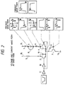
- Fig. 1 is a circuit diagram showing an example of a conventional semiconductor light emitting element driving circuit.
- this driving circuit consists of differentially connected bipolar transistors 1 and 2; a bipolar transistor 3 which operates with a constant current; a semiconductor light emitting element 4; a resistor 5; an inductance 6 of the line which connects the bipolar transistors for driving the semiconductor light emitting element and the semiconductor light emitting element; an inductance 7 of the line which connects the semiconductor light emitting element and a power supply; a junction capacitance 8 of the semiconductor light emitting element; collector-emitter capacitances 9 and 10 of the bipolar transistors 1 and 2, respectively; and a base-collector capacitance 11 of the bipolar transistor 3.
- the emitters of the differentially connected bipolar transistors 1 and 2 are connected to the collector of the bipolar transistor 3 which has the same conductivity type and operates as a constant current source.
- Fig. 2 is a view for explaining the mechanism in which the driving current for the semiconductor light emitting element is distorted in the configuration illustrated in Fig. 1. This mechanism will be described below with reference to Fig. 2.
- the semiconductor light emitting element 4 needs to be switched at a high speed with a constant current of about a few milliamperes to 100 milliamperes. Assume that the value of this constant current is I and the values of the inductances 6 and 7 are L1 and L2, respectively.
- This distortion in the waveform is represented by overshoot or ringing. If overshoot takes place, a semiconductor light emitting element deteriorates, and this consequently reduces the life of a product using this semiconductor light emitting element.
- a snubber circuit consisting of a resistor 12 and a capacitor 13 is additionally provided externally to the package incorporating a semiconductor light emitting element driving circuit.
- the emitters that are differentially connected and the base and collector of a transistor which operates with a constant current are extracted to terminals, and a coil 14 or a capacitor 15 is inserted to stabilize the constant current.
- connecting terminals are denoted by 19, 20, 21, and 22.
- the first invention of this application solves this problem.
- Fig. 5 is an equivalent circuit diagram of this prior art which includes parasitic elements (parasitic inductance components).
- Fig. 6 shows the packaged state of the circuit shown in Fig. 5.
- this circuit includes differentially connected bipolar transistors 1 and 2 formed in the integrated circuit 117; a constant current source 3; a semiconductor light emitting element 4; a resistor 5; a parasitic inductance 106 of the bonding wire for connecting the collectors of the bipolar transistors for driving the semiconductor light emitting element to the pin of the package 116; a parasitic inductance 107 of the pin; a parasitic inductance 108 of the lingo from the pin to the semiconductor light emitting element 4; the resistor 109; the capacitor 110; a parasitic inductance 112 resulting from the series connection of the resistor 109 and the capacitor 110; a power supply 15; complementary pulse signals 114 and 115 for driving the transistors 1 and 2; and the integrated circuit 117 including the transistors 1 and 2.
- a semiconductor light emitting element needs to be switched at a high speed with a constant current of about a few milliamperes to 100 milliamperes. Assume that the value of this constant current is I and the values of the parasitic inductances 106, 107, 108, and 112 are L1, L2, L3, and L4, respectively.
- Equation 9 I + ( ⁇ 1t)th power of K1 ⁇ e + ( ⁇ 2t)th power of K2 ⁇ e
- ⁇ 0 1/ ⁇ (L3 + L4)C)
- ⁇ 2(L3 + L4)/R
- ⁇ f ⁇ ( ⁇ 02 - ⁇ 2)
- i1 I[1 - ⁇ -(t/ ⁇ )th power of ⁇ 0/ ⁇ s ⁇ e ⁇ sin( ⁇ f t + ⁇ )]
- i1 I ⁇ 1 + (-t/ ⁇ )th power of (1 + t/ ⁇ ) ⁇ e ⁇ .
- the waveforms of the current flowing through the semiconductor light emitting element are as indicated by (a), (b), and (c), respectively, in Figs. 8A to 8C.
- the waveform shown in Fig. 8A degrades the life of the semiconductor light emitting element because of occurrence of overshoot, leading to a short product life.
- the waveform shown in Fig. 8B increases the rise time to make high-speed switching impossible.
- the most desired waveform is as illustrated in Fig. 8C.
- the second invention of this application solves the above problem.
- An embodiment of the present invention realizes a semiconductor light emitting element driving circuit capable of driving a semiconductor light emitting element with a stable driving current by eliminating distortion of the waveform of the driving current for the semiconductor light emitting element, thereby preventing deterioration of the semiconductor light emitting element and increasing the life of a product.
- An embodiment of the present invention provides a semiconductor light emitting element driving circuit capable of preventing a decrease in the driving frequency or increases in the number of package pins and the number of parts.
- An embodiment of the present invention provides a semiconductor light emitting element driving circuit for driving a light emitting element, comprising a bipolar transistor, the base of which is applied with a control signal for driving the light emitting element, and which, in response to the control signal, drives the light emitting element by flowing a current between the emitter and the collector, and a gate insulated transistor which operates as a constant current source connected to the bipolar transistor.
- An embodiment of the present invention provides a semiconductor light emitting element driving circuit for driving a light emitting element, comprising a bipolar transistor, the base of which is applied with a control signal for driving the light emitting element, and which, in response to the control signal, drives the light emitting element by flowing a current between the emitter and the collector, a constant current source connected to the bipolar transistor, and a series circuit inserted into a line between the bipolar transistor and the light emitting element and consisting of a resistor and a capacitor, wherein the bipolar transistor, the constant current source, and the series circuit are integrated into a single chip.
- An embodiment of the present invention provide a circuit which uses as its means a semiconductor light emitting element driving circuit which is a semiconductor integrated circuit in which differentially connected bipolar transistors and a MOS transistor are formed on the same substrate, and has a semiconductor light emitting element connected to and driven by the collectors of the differentially connected bipolar transistors, wherein the emitters of the differentially connected bipolar transistors are connected to the drain of the MOS transistor which operates as a constant current source and has the same conductivity type as that of the bipolar transistors.
- the circuit can prevent overshoot or ringing taking place in the driving current of the semiconductor light emitting element by controlling the response of the constant current source by using a MOS transistor whose mutual conductance is small.
- An embodiment of the present invention provide a circuit in which a series circuit consisting of a resistor and a capacitor is formed in an integrated circuit, in which bipolar transistors are formed, and is connected between the collectors of the bipolar transistors and a power supply or a substrate potential. With this arrangement, the circuit can effectively suppress overshoot and prevent a decrease in the operating speed.
- a basic arrangement of the present invention is a driving circuit comprising a bipolar transistor which is applied with a control signal for driving a light emitting element, and a constant current source for supplying a constant current to the bipolar transistor.
- the bipolar transistor When an ON signal is applied as the control signal, the bipolar transistor is turned on to flow a current between the emitter and the base. This current is for driving the light emitting element and supplied from the constant current source.
- One embodiment of the first invention of this application is a semiconductor light emitting element driving circuit which is a semiconductor integrated circuit having differentially connected bipolar transistors and a MOS transistor on the same substrate, which uses the differentially connected bipolar transistors as a switching circuit, and which has a light emitting element connected to and driven by the bipolar transistors.
- a constant current circuit using a MOS transistor is connected to the differentially connected bipolar transistors.
- This driving circuit is also characterized in that a plurality of MOS transistors are connected in parallel.
- a MOS transistor such as one formed in the same integrated circuit as bipolar transistors as in the present invention, excluding those fabricated through some special process, such as power MOS transistors, is primarily used in a logical circuit. Therefore, a current which a MOS transistor handles is commonly 1 ⁇ A or lower. Consequently, a very large MOS transistor is necessary to obtain a current of several milliamperes to 100 milliamperes for driving a semiconductor light emitting element.
- the dimensions of such a MOS transistor obtained by simulation are a gate width of 2000 ⁇ m and a gate length of 3 ⁇ m. A MOS transistor of this size can no longer be handled as a lumped constant, so the current density sometimes varies in the transistor. To prevent this, it is preferable to connect a plurality of MOS transistors in parallel.
- a semiconductor light emitting element driving circuit is characterized in that a time constant circuit formed in the same integrated circuit as the MOS transistor used as a constant current source and consisting of a resistor and a capacitor is connected to the gate of the MOS transistor.
- a semiconductor light emitting element driving circuit is characterized in that the base of the bipolar transistor is driven upon being applied with a complementary signal. Consequently, the bipolar transistor is switched without being saturated. This allows current switching at the highest speed.
- a MOS transistor is used as a constant current source connected to the emitters of differentially connected bipolar transistors, and, if necessary, a time constant circuit consisting of a resistor and a capacitor is connected to the gate of the MOS transistor. This makes it possible to obtain a high-speed current pulse waveform free from overshoot and ringing.
- a switching circuit consisting of a pair of differentially connected bipolar transistors and a series circuit consisting of a resistor and a capacitor are integrated into a one-chip IC.
- This circuit is more preferably a driving circuit in which a driving means having a switching circuit consisting of a pair of differentially connected bipolar transistors and a constant current circuit constituted by a MOS transistor is connected to the cathode of a light emitting element.
- a driving means having a switching circuit consisting of a pair of differentially connected bipolar transistors and a constant current circuit constituted by a MOS transistor is connected to the cathode of a light emitting element.
- the series circuit of the resistor and the capacitor is connected to the cathode of the light emitting element, and the driving circuit and the series circuit are integrated into one chip.
- driving circuits can be realized as a one-chip IC by using well-known IC process techniques. It is also possible to fabricate the circuits by using a compound semiconductor such as gallium arsenide or indium phosphorus. When a driving circuit is to be fabricated by using the same compound semiconductor as a light emitting element, it is readily possible to integrate the two into one chip.
- Fig. 9 is a circuit diagram showing a semiconductor light emitting element driving circuit according to the first embodiment of the present invention.
- npn transistors 1 and 2 are differentially connected.
- An NMOS transistor 3 has a drain connected to the common emitter of the npn transistors 1 and 2 and operates with a constant current.
- a semiconductor light emitting element 4 has a cathode connected to the collector of the npn transistor 1 via a parasitic inductance 6 of a line.
- a resistor 5 as a load is connected to the collector of the npn transistor 2.
- a parasitic inductance 7 is due to the line between the anode of the semiconductor light emitting element 4 and a power supply 15 as a high-potential reference voltage source.
- the semiconductor light emitting element 4 has a junction capacitance C j , 8.
- the npn transistors 1 and 2 have emitter-collector capacitances 9 and 10, respectively.
- the NMOS transistor 3 which operates as a constant current source has a drain-gate capacitance 11.
- One end of a resistor 12 is connected to the gate of the NMOS transistor 3 and to one end of a capacitor 13.
- the other end of the resistor 12 is connected to the gate and drain of an NMOS transistor 14 for applying a bias potential.
- the other end of the capacitor 13 is connected to a ground potential 16 as a low-potential reference voltage source.
- Inverters 17 and 18 supply complementary switching signals to the bases of the differentially connected npn transistors.
- a constant current source 19 supplies a constant current to the NMOS transistor 14.
- Fig. 10 is a view showing voltage waveforms and current waveforms at individual nodes in the first embodiment. The operation of this embodiment will be described below with reference to Fig. 10.
- the inverter 17 applies a High-level signal to the base of the npn transistor 1, and the inverter 18 applies a Low-level signal to the base of the npn transistor 2. Consequently, the npn transistor 1 is activated, and the npn transistor 2 is cut off.
- the collector current of the npn transistor 1, i.e., the driving current of the semiconductor light emitting element changes from 0 to a drain current I of the NMOS transistor 3, which operates with a constant current, in a certain time t. As indicated by (a) and (b) in Fig.
- These counterelectromotive voltage pulses are transmitted to the gate of the NMOS transistor 3 through the junction capacitance 8 of the semiconductor light emitting element, the emitter-collector capacitance 9 of the npn transistor 1, and the gate-drain capacitance 11 of the NMOS transistor 3.
- Potential variations at the emitters of the npn transistors 1 and 2 are illustrated in (e) of Fig.
- Figs. 11A to 11C indicate the driving current waveforms of the semiconductor light emitting element and gate voltage waveforms obtained while changing the time constant obtained by the resistor 12 and the capacitor 13 connected to the gate of the NMOS transistor 3 which operates with a constant current.
- Figs. 11A to 11C show that when the time constant is made most suitable, a current waveform free from overshoot and ringing can be obtained.
- MOS transistor 3 it is preferable to realized a MOS transistor 3 by connecting MOS transistors in parallel, which are individually formed in a plurality of active regions formed on an Si substrate and isolated by a field insulating film made from SiO2 as a dielectric substance.
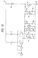
- Fig. 12 is a circuit diagram showing a semiconductor light emitting element driving circuit according to the second embodiment of the present invention.
- a plurality of NMOS transistors are connected in parallel, and a resistor and a capacitor are connected to the gate of each MOS transistor.
- a MOS transistor is used as a constant current source connected to the emitters of differentially connected bipolar transistors. Additionally, a time constant circuit consisting of a resistor and a capacitor is connected to the gate of this MOS transistor. Consequently, it is possible to obtain a current pulse waveform free from overshoot and ringing.
- Fig. 13 is a circuit diagram showing the semiconductor light emitting element driving circuit.
- this driving circuit comprises differentially connected bipolar transistors 1 and 2 formed in an integrated circuit (not shown), a constant current source 3, a semiconductor light emitting element 4, a resistor 5, parasitic inductances 106, 107, and 108, a resistor 109, and a capacitor 110.
- the parasitic inductance 106 is due to the bonding wire connecting the collectors of the bipolar transistors for driving the semiconductor light emitting element to the pin of a package 116.
- the parasitic inductance 107 is due to the pin, and the parasitic resistance 108 is derived from the line from the pin to the semiconductor light emitting element 4.
- the resistor 109 is formed in the integrated circuit in which the bipolar transistors are formed.
- the capacitor 110 is also formed in the same integrated circuit.
- the resistor 109 and the capacitor 110 are connected in series in the integrated circuit.
- One terminal of this series circuit is connected to the collectors of the bipolar transistors for driving the semiconductor light emitting element.
- the other terminal of the series circuit is connected to a power supply 15 or a substrate potential.
- the transistors 1 and 2 are driven by complementary signals 114 and 115, respectively.
- the current flowing through the semiconductor light emitting element when complementary pulse signals are applied to the semiconductor light emitting element driving circuit can be set in a critical state which is between the state in which the current varies in an oscillating manner and the state in which the current varies in an unoscillating manner.
- a constant current circuit denoted by reference numeral 3 in Fig. 13 is constituted by MOS transistors such as shown in Fig. 12.
- a series circuit which consists of a resistor and a capacitor and is conventionally arranged outside an integrated circuit in which bipolar transistors are formed is directly connected to the collectors of the bipolar transistors in the integrated circuit. Therefore, a parasitic inductance that is produced in conventional circuits is not generated between the collectors of the bipolar circuits for driving the semiconductor light emitting element and the series circuit.
- the current flowing through the semiconductor light emitting element when complementary pulse signals are applied to the semiconductor light emitting element driving circuit can be set in a critical state which is between the state in which the current varies in an oscillating manner and the state in which the current varies in an unoscillating manner. With this setting, it is possible to prevent overshoot and perform high-speed switching in the semiconductor light emitting element driving circuit.
- Fig. 14 is a sectional view showing a portion of an IC chip in which the driving circuit of the present invention is formed.
- Fig. 14 only one bipolar transistor BPT and two MOS transistors MOS are illustrated, and other components such as a protective layer are omitted.
- the parts shown in Fig. 14 are a p-type silicon substrate 201, an n+-type collector buried layer 202, a p-type well 203, an n ⁇ -type epitaxial layer 204, a p-type base 205, and an n+-type emitter 206.
- the two NMOS transistors MOS have sources/drains 207 and 208 and gates 210.
- a field insulating film 209 isolates the elements.
- a collector line 211 of the bipolar transistor is connected to the terminal of a light emitting element.
- a base line 212 serves as an input terminal, and a line 213 connects a constant current source to the bipolar transistor.
- a ground line 214 is connected to a low-potential reference voltage source.
- Fig. 15 is a sectional view showing a portion of an IC chip in which a series circuit of a resistor R and a capacitor C is formed.
- n+-type diffusion layers 221 and 222 are formed, and a series connecting line 215 connects the resistor R and the capacitor C.
- the circuit also includes an insulating interlayer 230.
- a driving circuit is formed into a single chip as illustrated in Fig. 14 by a fabrication method called a BiMOS process or a BiCMOS process. If necessary, the series circuit shown in Fig. 15 is also monolithically integrated with the driving circuit.
- Figs. 16A and 16B illustrate examples of systems using the circuit of the present invention.
- Fig. 16A shows a printer
- Fig. 16B shows an optical communication system.
- the printer shown in Fig. 16A comprises a photosensitive drum DRM, a cleaner CLN, a charger CGR, and an exposure unit EXP which employs the driving circuit of the present invention, a developing unit DVLP, and a recording medium P.
- the exposure unit EXP uses an LED array or a laser diode as a light emitting element and forms latent images on the photosensitive drum by using light from the light emitting element.
- the transmission side includes a laser diode LD as a light emitting element and a transmitter SYS1 with a driving circuit
- the reception side includes a photodiode sensor PHD and a receiver SYS2.
- An optical fiber OFR also is provided.
- the present invention is adopted in the transmitter SYS1.
Landscapes
- Physics & Mathematics (AREA)
- Optics & Photonics (AREA)
- Electromagnetism (AREA)
- Engineering & Computer Science (AREA)
- Plasma & Fusion (AREA)
- Led Devices (AREA)
- Printers Or Recording Devices Using Electromagnetic And Radiation Means (AREA)
Priority Applications (1)
| Application Number | Priority Date | Filing Date | Title |
|---|---|---|---|
| EP98203404A EP0905900B1 (de) | 1994-04-22 | 1995-04-13 | Treiberschaltung für eine Leuchtdiode |
Applications Claiming Priority (4)
| Application Number | Priority Date | Filing Date | Title |
|---|---|---|---|
| JP84576/94 | 1994-04-22 | ||
| JP8457694 | 1994-04-22 | ||
| JP147080/94 | 1994-06-06 | ||
| JP14708094 | 1994-06-06 |
Related Child Applications (1)
| Application Number | Title | Priority Date | Filing Date |
|---|---|---|---|
| EP98203404A Division EP0905900B1 (de) | 1994-04-22 | 1995-04-13 | Treiberschaltung für eine Leuchtdiode |
Publications (3)
| Publication Number | Publication Date |
|---|---|
| EP0678982A2 true EP0678982A2 (de) | 1995-10-25 |
| EP0678982A3 EP0678982A3 (de) | 1996-03-06 |
| EP0678982B1 EP0678982B1 (de) | 1999-03-31 |
Family
ID=26425592
Family Applications (2)
| Application Number | Title | Priority Date | Filing Date |
|---|---|---|---|
| EP95302505A Expired - Lifetime EP0678982B1 (de) | 1994-04-22 | 1995-04-13 | Treiberschaltung für ein lichtemittierendes Halbleiterelement |
| EP98203404A Expired - Lifetime EP0905900B1 (de) | 1994-04-22 | 1995-04-13 | Treiberschaltung für eine Leuchtdiode |
Family Applications After (1)
| Application Number | Title | Priority Date | Filing Date |
|---|---|---|---|
| EP98203404A Expired - Lifetime EP0905900B1 (de) | 1994-04-22 | 1995-04-13 | Treiberschaltung für eine Leuchtdiode |
Country Status (6)
| Country | Link |
|---|---|
| US (1) | US5739717A (de) |
| EP (2) | EP0678982B1 (de) |
| KR (1) | KR100191060B1 (de) |
| CN (1) | CN1050719C (de) |
| DE (2) | DE69508639T2 (de) |
| TW (1) | TW330355B (de) |
Cited By (5)
| Publication number | Priority date | Publication date | Assignee | Title |
|---|---|---|---|---|
| GB2301700A (en) * | 1995-05-31 | 1996-12-11 | Eastman Kodak Co | A laser writer drive circuit |
| EP0798618A1 (de) * | 1996-03-29 | 1997-10-01 | Kabushiki Kaisha Toshiba | Array-Anordnung mit Schaltkreisen und Konstantstromquellen für eine Vielzahl von Kanälen |
| EP0933971A2 (de) * | 1998-01-30 | 1999-08-04 | Canon Kabushiki Kaisha | Steuergerät für Lichtquelle |
| EP1496503A1 (de) * | 2002-04-18 | 2005-01-12 | TDK Corporation | Halbleiterlaseransteuerschaltung und optischer kopf |
| EP1381036A3 (de) * | 2002-07-03 | 2006-07-12 | Ricoh Company, Ltd. | Lichtquellenansteuerschaltung, optisches Informationsaufzeichnungsgerät und optisches Informationsaufzeichnungsverfahren |
Families Citing this family (12)
| Publication number | Priority date | Publication date | Assignee | Title |
|---|---|---|---|---|
| US6091531A (en) * | 1998-01-30 | 2000-07-18 | Motorola, Inc. | Differential charge and dump optoelectronic receiver |
| JP4238410B2 (ja) * | 1999-04-09 | 2009-03-18 | ソニー株式会社 | 情報処理システム |
| US6728494B2 (en) * | 2000-06-08 | 2004-04-27 | Matsushita Electric Industrial Co., Ltd. | Light-emitting device drive circuit, and optical transmission system using the circuit |
| TWI223900B (en) * | 2003-07-31 | 2004-11-11 | United Epitaxy Co Ltd | ESD protection configuration and method for light emitting diodes |
| JP2005294758A (ja) * | 2004-04-05 | 2005-10-20 | Toshiba Corp | 発光素子駆動回路 |
| KR101061847B1 (ko) | 2004-08-20 | 2011-09-02 | 삼성전자주식회사 | 전원 공급 장치 및 백라이트 장치 |
| JP2007081009A (ja) * | 2005-09-13 | 2007-03-29 | Matsushita Electric Ind Co Ltd | 駆動回路およびデータ線ドライバ |
| CN100514776C (zh) * | 2007-08-22 | 2009-07-15 | 中国科学院上海光学精密机械研究所 | 连续可调纳秒脉冲半导体激光器驱动电源 |
| JP5344005B2 (ja) * | 2011-06-07 | 2013-11-20 | 株式会社豊田自動織機 | スイッチング回路 |
| CN104393861B (zh) * | 2014-11-27 | 2017-12-19 | 大连尚能科技发展有限公司 | 一种mosfet的并联电路 |
| CN108627845B (zh) * | 2017-03-15 | 2021-05-28 | 信泰光学(深圳)有限公司 | 雷射驱动电路的电路布局结构 |
| EP3435428B1 (de) * | 2017-07-26 | 2019-11-27 | ams AG | Lichtemittierendes halbleiterbauelement zur erzeugung von kurzen lichtimpulsen |
Citations (14)
| Publication number | Priority date | Publication date | Assignee | Title |
|---|---|---|---|---|
| US4539686A (en) * | 1982-10-15 | 1985-09-03 | At&T Bell Laboratories | Laser driving means |
| EP0186385A2 (de) * | 1984-12-24 | 1986-07-02 | Unisys Corporation | Integrierte logische Schaltung mit Modul zur Erzeugung eines Steuersignals zur Aufhebung von Schaltgeräuschen |
| US4709370A (en) * | 1985-06-17 | 1987-11-24 | Rca Corporation | Semiconductor laser driver circuit |
| JPS62273787A (ja) * | 1986-05-21 | 1987-11-27 | Matsushita Electric Ind Co Ltd | 発光素子駆動回路 |
| JPS6433976A (en) * | 1987-07-29 | 1989-02-03 | Nec Corp | Light output changing circuit |
| JPH01261918A (ja) * | 1988-04-13 | 1989-10-18 | Hitachi Ltd | 半導体回路 |
| JPH0258881A (ja) * | 1988-08-25 | 1990-02-28 | Canon Inc | 発光素子駆動装置 |
| JPH02296382A (ja) * | 1989-05-11 | 1990-12-06 | Mitsubishi Electric Corp | 半導体発光素子の駆動回路 |
| JPH03171687A (ja) * | 1989-11-29 | 1991-07-25 | Matsushita Electric Ind Co Ltd | レーザダイオード駆動装置 |
| EP0469244A2 (de) * | 1990-08-02 | 1992-02-05 | Sumitomo Electric Industries, Ltd. | Treiberschaltung für ein lichtemittierendes Element |
| JPH04219985A (ja) * | 1990-12-19 | 1992-08-11 | Nec Corp | 発光素子駆動回路 |
| WO1993017498A1 (en) * | 1992-02-27 | 1993-09-02 | Microunity Systems Engineering, Inc. | BiCMOS LOGIC CIRCUIT |
| EP0563580A2 (de) * | 1992-02-28 | 1993-10-06 | Canon Kabushiki Kaisha | Steuerschaltung für lichtemittierende Vorrichtung |
| EP0583688A1 (de) * | 1992-08-18 | 1994-02-23 | Siemens Aktiengesellschaft | Digitaler Stromschalter |
Family Cites Families (9)
| Publication number | Priority date | Publication date | Assignee | Title |
|---|---|---|---|---|
| US4581542A (en) * | 1983-11-14 | 1986-04-08 | General Electric Company | Driver circuits for emitter switch gate turn-off SCR devices |
| JPH0732261B2 (ja) * | 1985-04-11 | 1995-04-10 | キヤノン株式会社 | 半導体受光装置 |
| JPS61258486A (ja) * | 1985-05-11 | 1986-11-15 | Canon Inc | レ−ザ−駆動装置 |
| JPH02205380A (ja) * | 1989-02-03 | 1990-08-15 | Canon Inc | 発光素子駆動回路 |
| JP2774189B2 (ja) * | 1989-11-22 | 1998-07-09 | キヤノン株式会社 | 直結型ベース接地増幅器及び該増幅器を含む回路装置、半導体装置並びに情報処理装置 |
| JPH04174582A (ja) * | 1990-11-07 | 1992-06-22 | Nec Corp | マーク率検出回路 |
| US5124580A (en) * | 1991-04-30 | 1992-06-23 | Microunity Systems Engineering, Inc. | BiCMOS logic gate having linearly operated load FETs |
| JP3110502B2 (ja) * | 1991-07-31 | 2000-11-20 | キヤノン株式会社 | カレント・ミラー回路 |
| US5341042A (en) * | 1992-08-10 | 1994-08-23 | International Business Machines Corporation | Low voltage, cascoded NTL based BiCMOS circuit |
-
1995
- 1995-04-13 DE DE69508639T patent/DE69508639T2/de not_active Expired - Lifetime
- 1995-04-13 EP EP95302505A patent/EP0678982B1/de not_active Expired - Lifetime
- 1995-04-13 DE DE69525865T patent/DE69525865T2/de not_active Expired - Lifetime
- 1995-04-13 EP EP98203404A patent/EP0905900B1/de not_active Expired - Lifetime
- 1995-04-17 TW TW084103747A patent/TW330355B/zh not_active IP Right Cessation
- 1995-04-19 US US08/424,179 patent/US5739717A/en not_active Expired - Lifetime
- 1995-04-22 KR KR1019950009493A patent/KR100191060B1/ko not_active IP Right Cessation
- 1995-04-22 CN CN95104505A patent/CN1050719C/zh not_active Expired - Fee Related
Patent Citations (14)
| Publication number | Priority date | Publication date | Assignee | Title |
|---|---|---|---|---|
| US4539686A (en) * | 1982-10-15 | 1985-09-03 | At&T Bell Laboratories | Laser driving means |
| EP0186385A2 (de) * | 1984-12-24 | 1986-07-02 | Unisys Corporation | Integrierte logische Schaltung mit Modul zur Erzeugung eines Steuersignals zur Aufhebung von Schaltgeräuschen |
| US4709370A (en) * | 1985-06-17 | 1987-11-24 | Rca Corporation | Semiconductor laser driver circuit |
| JPS62273787A (ja) * | 1986-05-21 | 1987-11-27 | Matsushita Electric Ind Co Ltd | 発光素子駆動回路 |
| JPS6433976A (en) * | 1987-07-29 | 1989-02-03 | Nec Corp | Light output changing circuit |
| JPH01261918A (ja) * | 1988-04-13 | 1989-10-18 | Hitachi Ltd | 半導体回路 |
| JPH0258881A (ja) * | 1988-08-25 | 1990-02-28 | Canon Inc | 発光素子駆動装置 |
| JPH02296382A (ja) * | 1989-05-11 | 1990-12-06 | Mitsubishi Electric Corp | 半導体発光素子の駆動回路 |
| JPH03171687A (ja) * | 1989-11-29 | 1991-07-25 | Matsushita Electric Ind Co Ltd | レーザダイオード駆動装置 |
| EP0469244A2 (de) * | 1990-08-02 | 1992-02-05 | Sumitomo Electric Industries, Ltd. | Treiberschaltung für ein lichtemittierendes Element |
| JPH04219985A (ja) * | 1990-12-19 | 1992-08-11 | Nec Corp | 発光素子駆動回路 |
| WO1993017498A1 (en) * | 1992-02-27 | 1993-09-02 | Microunity Systems Engineering, Inc. | BiCMOS LOGIC CIRCUIT |
| EP0563580A2 (de) * | 1992-02-28 | 1993-10-06 | Canon Kabushiki Kaisha | Steuerschaltung für lichtemittierende Vorrichtung |
| EP0583688A1 (de) * | 1992-08-18 | 1994-02-23 | Siemens Aktiengesellschaft | Digitaler Stromschalter |
Non-Patent Citations (7)
| Title |
|---|
| PATENT ABSTRACTS OF JAPAN vol. 12, no. 162 (E-609) (3009) 17 May 1988 & JP-A-62 273 787 (MATSUSHITA ELECTRIC IND CO LTD) 27 November 1987 * |
| PATENT ABSTRACTS OF JAPAN vol. 13, no. 226 (E-763) 25 May 1989 & JP-A-01 033 976 (NEC CORP) 3 February 1989 * |
| PATENT ABSTRACTS OF JAPAN vol. 14, no. 18 (E-873) (3961) 16 January 1990 & JP-A-01 261 918 (HITACHI LTD) 18 October 1989 * |
| PATENT ABSTRACTS OF JAPAN vol. 14, no. 229 (E-0928) 15 May 1990 & JP-A-02 058 881 (CANON INC) 28 February 1990 * |
| PATENT ABSTRACTS OF JAPAN vol. 15, no. 412 (E-1124) 21 October 1991 & JP-A-03 171 687 (MATSUSHITA ELECTRIC IND CO LTD) 25 July 1991 * |
| PATENT ABSTRACTS OF JAPAN vol. 15, no. 78 (E-1037) 22 February 1991 & JP-A-02 296 382 (MITSUBISHI ELECTRIC CORP) 6 December 1990 * |
| PATENT ABSTRACTS OF JAPAN vol. 16, no. 567 (E-1296) 8 December 1992 & JP-A-04 219 985 (NEC CORP) 11 August 1992 * |
Cited By (12)
| Publication number | Priority date | Publication date | Assignee | Title |
|---|---|---|---|---|
| GB2301700A (en) * | 1995-05-31 | 1996-12-11 | Eastman Kodak Co | A laser writer drive circuit |
| US5598040A (en) * | 1995-05-31 | 1997-01-28 | Eastman Kodak Company | Laser writer having high speed high current laser driver |
| GB2301700B (en) * | 1995-05-31 | 1999-03-10 | Eastman Kodak Co | Laser writer having high speed, high current laser driver |
| EP0798618A1 (de) * | 1996-03-29 | 1997-10-01 | Kabushiki Kaisha Toshiba | Array-Anordnung mit Schaltkreisen und Konstantstromquellen für eine Vielzahl von Kanälen |
| US5883546A (en) * | 1996-03-29 | 1999-03-16 | Kabushiki Kaisha Toshiba | Array device having functional circuit for a plurality of channels |
| EP0933971A2 (de) * | 1998-01-30 | 1999-08-04 | Canon Kabushiki Kaisha | Steuergerät für Lichtquelle |
| EP0933971A3 (de) * | 1998-01-30 | 2000-10-18 | Canon Kabushiki Kaisha | Steuergerät für Lichtquelle |
| EP1496503A1 (de) * | 2002-04-18 | 2005-01-12 | TDK Corporation | Halbleiterlaseransteuerschaltung und optischer kopf |
| EP1496503A4 (de) * | 2002-04-18 | 2008-05-14 | Tdk Corp | Halbleiterlaseransteuerschaltung und optischer kopf |
| EP1381036A3 (de) * | 2002-07-03 | 2006-07-12 | Ricoh Company, Ltd. | Lichtquellenansteuerschaltung, optisches Informationsaufzeichnungsgerät und optisches Informationsaufzeichnungsverfahren |
| US7193957B2 (en) | 2002-07-03 | 2007-03-20 | Ricoh Company, Ltd. | Light source drive, optical information recording apparatus, and optical information recording method |
| US7480230B2 (en) | 2002-07-03 | 2009-01-20 | Ricoh Company, Ltd. | Light source drive, optical information recording apparatus, and optical information recording method |
Also Published As
| Publication number | Publication date |
|---|---|
| DE69508639T2 (de) | 1999-09-30 |
| TW330355B (en) | 1998-04-21 |
| EP0678982B1 (de) | 1999-03-31 |
| DE69508639D1 (de) | 1999-05-06 |
| EP0678982A3 (de) | 1996-03-06 |
| EP0905900A1 (de) | 1999-03-31 |
| KR100191060B1 (ko) | 1999-06-15 |
| US5739717A (en) | 1998-04-14 |
| CN1112752A (zh) | 1995-11-29 |
| KR950030421A (ko) | 1995-11-24 |
| EP0905900B1 (de) | 2002-03-13 |
| DE69525865D1 (de) | 2002-04-18 |
| DE69525865T2 (de) | 2002-09-19 |
| CN1050719C (zh) | 2000-03-22 |
Similar Documents
| Publication | Publication Date | Title |
|---|---|---|
| EP0678982A2 (de) | Treiberschaltung für ein lichtemittierendes Halbleiterelement | |
| EP0621694B1 (de) | Schnittstellenschaltung mit niedrigem Verbrauch | |
| US7411987B2 (en) | System and method for using an output transformer for laser diode drivers | |
| Rein et al. | A versatile Si-bipolar driver circuit with high output voltage swing for external and direct laser modulation in 10 Gb/s optical-fiber links | |
| KR100740359B1 (ko) | 전자 부품을 작동시키는 구동 회로 | |
| EP0542227B1 (de) | Ausgangspufferschaltung | |
| EP0798828A2 (de) | Treiberschaltung für lichtemittierendes Element und diese enthaltende lichtemittierende Vorrichtung | |
| EP0691742A2 (de) | Optischer Empfänger mit einem Vorverstärker hoher Impedanz | |
| US4718063A (en) | Optoelectronic integrated circuit multiplex | |
| JPH0560840A (ja) | インサーキツトテスト装置用ピンドライバ | |
| US6483345B1 (en) | High speed level shift circuit for low voltage output | |
| EP0854577A2 (de) | Integrierte Halbleiterschaltung | |
| US6049175A (en) | Arrangements relating to light emitting devices | |
| USRE35836E (en) | Solid state optically coupled electrical power switch | |
| JP3402839B2 (ja) | 半導体発光素子駆動回路 | |
| US6359465B1 (en) | CMOS small signal switchable adjustable impedence terminator network | |
| EP0810700A2 (de) | Auf-dem-Chip-Vorrichtung zum Dämpfen hoher Frequenzen für Treiberschaltungen | |
| JP3013894B2 (ja) | Fet装置 | |
| EP0886350B1 (de) | Hochgeschwindigkeitstreiber für nicht polarisierte Halbleiter-Diodenlaser bei Hochgeschwindigkeits-Digitalübertragung | |
| US5343099A (en) | Output device capable of high speed operation and operating method thereof | |
| JP3319879B2 (ja) | 半導体装置 | |
| JP2003234508A (ja) | 半導体発光素子駆動回路 | |
| EP0660513B1 (de) | Elektronische Schaltung zum Ersetzen einer lichtemittierenden Diode und eines lichtabhängigen Widerstandes | |
| WO1992000543A1 (en) | Bipolar junction transistor combined with an optical modulator | |
| JP2738598B2 (ja) | 光半導体素子の駆動回路 |
Legal Events
| Date | Code | Title | Description |
|---|---|---|---|
| PUAI | Public reference made under article 153(3) epc to a published international application that has entered the european phase |
Free format text: ORIGINAL CODE: 0009012 |
|
| AK | Designated contracting states |
Kind code of ref document: A2 Designated state(s): DE FR GB IT NL |
|
| PUAL | Search report despatched |
Free format text: ORIGINAL CODE: 0009013 |
|
| AK | Designated contracting states |
Kind code of ref document: A3 Designated state(s): DE FR GB IT NL |
|
| 17P | Request for examination filed |
Effective date: 19960717 |
|
| 17Q | First examination report despatched |
Effective date: 19970603 |
|
| GRAG | Despatch of communication of intention to grant |
Free format text: ORIGINAL CODE: EPIDOS AGRA |
|
| GRAG | Despatch of communication of intention to grant |
Free format text: ORIGINAL CODE: EPIDOS AGRA |
|
| GRAH | Despatch of communication of intention to grant a patent |
Free format text: ORIGINAL CODE: EPIDOS IGRA |
|
| GRAH | Despatch of communication of intention to grant a patent |
Free format text: ORIGINAL CODE: EPIDOS IGRA |
|
| GRAA | (expected) grant |
Free format text: ORIGINAL CODE: 0009210 |
|
| AK | Designated contracting states |
Kind code of ref document: B1 Designated state(s): DE FR GB IT NL |
|
| ITF | It: translation for a ep patent filed |
Owner name: SOCIETA' ITALIANA BREVETTI S.P.A. |
|
| REF | Corresponds to: |
Ref document number: 69508639 Country of ref document: DE Date of ref document: 19990506 |
|
| ET | Fr: translation filed | ||
| PLBE | No opposition filed within time limit |
Free format text: ORIGINAL CODE: 0009261 |
|
| STAA | Information on the status of an ep patent application or granted ep patent |
Free format text: STATUS: NO OPPOSITION FILED WITHIN TIME LIMIT |
|
| 26N | No opposition filed | ||
| REG | Reference to a national code |
Ref country code: GB Ref legal event code: IF02 |
|
| PGFP | Annual fee paid to national office [announced via postgrant information from national office to epo] |
Ref country code: NL Payment date: 20090427 Year of fee payment: 15 Ref country code: IT Payment date: 20090420 Year of fee payment: 15 Ref country code: FR Payment date: 20090424 Year of fee payment: 15 |
|
| REG | Reference to a national code |
Ref country code: NL Ref legal event code: V1 Effective date: 20101101 |
|
| REG | Reference to a national code |
Ref country code: FR Ref legal event code: ST Effective date: 20101230 |
|
| PG25 | Lapsed in a contracting state [announced via postgrant information from national office to epo] |
Ref country code: NL Free format text: LAPSE BECAUSE OF NON-PAYMENT OF DUE FEES Effective date: 20101101 Ref country code: FR Free format text: LAPSE BECAUSE OF NON-PAYMENT OF DUE FEES Effective date: 20100430 |
|
| PG25 | Lapsed in a contracting state [announced via postgrant information from national office to epo] |
Ref country code: IT Free format text: LAPSE BECAUSE OF NON-PAYMENT OF DUE FEES Effective date: 20100413 |
|
| PGFP | Annual fee paid to national office [announced via postgrant information from national office to epo] |
Ref country code: GB Payment date: 20140414 Year of fee payment: 20 |
|
| PGFP | Annual fee paid to national office [announced via postgrant information from national office to epo] |
Ref country code: DE Payment date: 20140430 Year of fee payment: 20 |
|
| REG | Reference to a national code |
Ref country code: DE Ref legal event code: R071 Ref document number: 69508639 Country of ref document: DE |
|
| REG | Reference to a national code |
Ref country code: GB Ref legal event code: PE20 Expiry date: 20150412 |
|
| PG25 | Lapsed in a contracting state [announced via postgrant information from national office to epo] |
Ref country code: GB Free format text: LAPSE BECAUSE OF EXPIRATION OF PROTECTION Effective date: 20150412 |