EP0676866A2 - Phasendetektor für einen Phasenregelkreis - Google Patents
Phasendetektor für einen Phasenregelkreis Download PDFInfo
- Publication number
- EP0676866A2 EP0676866A2 EP95104509A EP95104509A EP0676866A2 EP 0676866 A2 EP0676866 A2 EP 0676866A2 EP 95104509 A EP95104509 A EP 95104509A EP 95104509 A EP95104509 A EP 95104509A EP 0676866 A2 EP0676866 A2 EP 0676866A2
- Authority
- EP
- European Patent Office
- Prior art keywords
- signal
- phase
- flip
- flop
- state
- Prior art date
- Legal status (The legal status is an assumption and is not a legal conclusion. Google has not performed a legal analysis and makes no representation as to the accuracy of the status listed.)
- Granted
Links
Images

Classifications
-
- H—ELECTRICITY
- H04—ELECTRIC COMMUNICATION TECHNIQUE
- H04N—PICTORIAL COMMUNICATION, e.g. TELEVISION
- H04N5/00—Details of television systems
- H04N5/44—Receiver circuitry for the reception of television signals according to analogue transmission standards
- H04N5/455—Demodulation-circuits
-
- H—ELECTRICITY
- H04—ELECTRIC COMMUNICATION TECHNIQUE
- H04N—PICTORIAL COMMUNICATION, e.g. TELEVISION
- H04N5/00—Details of television systems
- H04N5/04—Synchronising
- H04N5/12—Devices in which the synchronising signals are only operative if a phase difference occurs between synchronising and synchronised scanning devices, e.g. flywheel synchronising
- H04N5/126—Devices in which the synchronising signals are only operative if a phase difference occurs between synchronising and synchronised scanning devices, e.g. flywheel synchronising whereby the synchronisation signal indirectly commands a frequency generator
-
- H—ELECTRICITY
- H03—ELECTRONIC CIRCUITRY
- H03L—AUTOMATIC CONTROL, STARTING, SYNCHRONISATION, OR STABILISATION OF GENERATORS OF ELECTRONIC OSCILLATIONS OR PULSES
- H03L7/00—Automatic control of frequency or phase; Synchronisation
- H03L7/06—Automatic control of frequency or phase; Synchronisation using a reference signal applied to a frequency- or phase-locked loop
- H03L7/08—Details of the phase-locked loop
- H03L7/085—Details of the phase-locked loop concerning mainly the frequency- or phase-detection arrangement including the filtering or amplification of its output signal
-
- H—ELECTRICITY
- H03—ELECTRONIC CIRCUITRY
- H03L—AUTOMATIC CONTROL, STARTING, SYNCHRONISATION, OR STABILISATION OF GENERATORS OF ELECTRONIC OSCILLATIONS OR PULSES
- H03L7/00—Automatic control of frequency or phase; Synchronisation
- H03L7/06—Automatic control of frequency or phase; Synchronisation using a reference signal applied to a frequency- or phase-locked loop
- H03L7/16—Indirect frequency synthesis, i.e. generating a desired one of a number of predetermined frequencies using a frequency- or phase-locked loop
- H03L7/18—Indirect frequency synthesis, i.e. generating a desired one of a number of predetermined frequencies using a frequency- or phase-locked loop using a frequency divider or counter in the loop
- H03L7/183—Indirect frequency synthesis, i.e. generating a desired one of a number of predetermined frequencies using a frequency- or phase-locked loop using a frequency divider or counter in the loop a time difference being used for locking the loop, the counter counting between fixed numbers or the frequency divider dividing by a fixed number
- H03L7/191—Indirect frequency synthesis, i.e. generating a desired one of a number of predetermined frequencies using a frequency- or phase-locked loop using a frequency divider or counter in the loop a time difference being used for locking the loop, the counter counting between fixed numbers or the frequency divider dividing by a fixed number using at least two different signals from the frequency divider or the counter for determining the time difference
Definitions
- the invention relates to an arrangement for generating a phase-lock-loop clock signal.
- Digital video signal processing systems with features such as on-screen display of text and picture-in-picture for both television receiver and video tape recorder signal sources may require a clock signal that is phase-locked to a horizontal synchronization signal, referred to as line-locked clock.
- line-locked clock a clock signal that is phase-locked to a horizontal synchronization signal
- PLL phase-locked loop
- phase error indicative signal may be independent of a duty cycle of the horizontal synchronization signal. It may also be desirable to generate the clock signal such that, in phase-lock condition, the edges of the clock and synchronization signals are aligned or occur approximately simultaneously. It may be further desirable to generate the phase error indicative signal such that the horizontal synchronization signal is applied to only one flip-flop in the phase detector and no signal path of the synchronizing signal includes another flip-flop in the phase detector. Thus, only one flip-flop is utilized both when the phase error is positive and negative. Thereby, the circuitry of the phase detector is simplified.
- a phase-lock-loop circuit embodying an aspect of the invention, includes a controllable oscillator and a source of a synchronizing signal.
- a flip-flop is responsive to the synchronizing signal for generating a flip-flop output signal at a first state when an edge of the synchronizing signal occurs. The output signal alternates between the first state and a second state.
- a decoder is used for applying the synchronizing signal to an output of said decoder via a signal path of the synchronizing signal that includes the flip-flop.
- a phase difference indicative signal is generated at the output of the decoder. The phase difference indicative signal is generated in accordance with a phase difference between the synchronizing signal and an output signal of the oscillator.
- phase difference that are both a positive and negative
- no other flip-flop is included in any signal path of the synchronizing signal between the source of synchronizing signal and the output of the decoder.
- a low-pass filter is responsive to the phase difference indicative signal and coupled to a control input of the oscillator for controlling the oscillator in a phase-lock-loop manner. In steady state phase-lock operation, an edge of the oscillator output signal is aligned with the edge of the synchronizing signal.
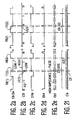
- FIGURE 1 illustrates a block diagram of a phase-lock loop circuit (PLL) 100, including a phase detector 101, embodying an aspect of the invention.
- a baseband luminance video signal VIDEO-IN obtained from, for example, a video detector, not shown, of a television receiver is coupled to a conventional sync separator 50 that generates pulses of a horizontal sync signal CSI having a period H at a horizontal deflection frequency f H that is in, for example, the NTSC standard 15,734 Hz.
- An output signal ClkDiv is produced at an output Q10, the most significant bit of eleven outputs Q0-Q10 of a divide-by-N binary counter 52, by frequency dividing an oscillatory output signal Clk of PLL 100 produced in a voltage-controlled-oscillator 53.
- Signal Clk may be used in various stages, not shown, of the television receiver for video signal processing. In steady state operation, the frequency of signal Clk is equal to N x f H .
- the value N denotes a ratio between the frequency of signal Clk and that of signal ClkDiv.
- the value N may be, for example, equal to 1716.
- FIGURES 2a-2f illustrate waveforms useful for explaining the operation of the circuit diagram of FIGURE 1. Similar symbols and numerals in FIGURES 1 and 2a-2f indicate similar items or functions.
- a clear input CLR of a storage element or D-type flip-flop 62 of FIGURE 1 receives a clear signal CLEAR at a LOW state developed at an output of a NAND gate 63.
- Signal CLEAR is developed, in a given period H of counter 52, when each of the ten least significant inverting signals developed at outputs Q0 ⁇ - Q9 ⁇ is at a HIGH state and signal ClkDiv, the most significant bit that is developed at non-inverting output Q10, is at a HIGH state.
- signal CLEAR of FIGURE 1 attains the LOW state.
- flip-flop 62 When signal CLEAR is at the LOW state, flip-flop 62 is latched to a reset state in which an output Q, where a signal SYN of FIGURE 2c is developed, is established at a LOW state and a signal SYN ⁇ developed an inverting output Q ⁇ of flip-flop 62 is at a HIGH state.
- Signal CLEAR provides initialization of flip-flop 62 in each horizontal period H.
- a leading edge LE(1) or LE(2), having a HIGH-TO-LOW transition, of a pulse of horizontal synchronization signal CSI of FIGURE 2b is produced when a horizontal sync pulse occurs in signal VIDEO-IN of FIGURE 1.
- signal CSI of FIGURE 2b is at a HIGH state.
- An input D of flip-flop 62 receives a signal VCC at a HIGH state.
- edge triggered flip-flop 62 of FIGURE 1 is latched to a set state in which output signal SYN of FIGURE 2c, developed at non-inverting output terminal Q of flip-flop 62 of FIGURE 1, attains a HIGH state.
- Signal ClkDiv has a trailing edge TC(1) or TC(2) of FIGURE 2a that is phase compared to signal SYN of FIGURE 2c.
- leading edge LE(1) shown at the left side of FIGURE 2b occurs when signal ClkDiv of FIGURE 2a is already at the HIGH state.
- the first example depicts a situation in which the phase of the pulse of signal CSI of FIGURE 2b, as determined by leading edge LE(1), lags the phase of signal ClkDiv of FIGURE 2a, as determined by a trailing edge TT(1) of signal ClkDiv. Consequently, an output signal 64a of FIGURE 1 of an AND gate 64 that receives signals SYN and ClkDiv is HIGH between edge LE(1) of FIGURE 2b and edge TT(1) of FIGURE 2a.
- Output signal 64a of FIGURE 1 is coupled via an OR gate 65 to an enable input 66a of a tri-state gate 66 to develop an enable signal ENA of FIGURE 2d at input 66a of FIGURE 1.
- Signal ClkDiv is coupled to an input 66b of gate 66.
- Signal ENA is at a HIGH state, between the time when edge LE(1) of FIGURE 2b occurs and the time when edge TT(1) of FIGURE 2a occurs. Therefore, signal ENA of FIGURE 1 causes signal ClkDiv that is also at the HIGH state to be coupled to an output 66c of gate 66 for developing an output signal OUT of FIGURES 1 and 2e at the HIGH state.
- a pulse of phase difference indicative signal OUT having a peak at the HIGH state is developed from signal ClkDiv.
- output 66c of FIGURE 1 is at a high impedance state.
- the pulse width of signal OUT is proportional to the phase error or difference.
- Signal OUT is coupled via a conventional low-pass filter 54 that forms the loop filter of PLL 100 to control input terminal 53a of oscillator 53 for controlling the phase and frequency of signal Clk.
- leading edge LE(2) shown at the right side of FIGURE 2a occurs when signal ClkDiv of FIGURE 2a is already at the LOW state.
- the second example depicts a situation in which the phase of signal CSI of FIGURE 2b, as determined by leading edge LE(2), lags the phase of signal ClkDiv of FIGURE 2a as determined by a trailing edge TT(2). Consequently, an output signal 67a of FIGURE 1 of an AND gate 67 that receives signals SYN ⁇ and ClkDiv ⁇ is HIGH between edge TT(2) of FIGURE 2a and edge LE(2) of FIGURE 2b.
- Output signal 67a of FIGURE 1 is coupled via OR gate 65 to enable input 66a of tristate gate 66 for developing enable signal ENA of FIGURE 2d at input 66a of FIGURE 1.
- Signal ClkDiv is coupled to input 66b of gate 66.
- Signal ENA is at a HIGH state, between the time when edge TT(2) of FIGURE 2a occurs and the time when edge LE(2) of FIGURE 2b occurs. Therefore, signal ENA of FIGURE 1 causes signal ClkDiv, that is at the LOW state, to be coupled to output 66c of gate 66. Consequently, output signal OUT of FIGURES 1 and 2e is developed at the LOW state.
- a pulse of phase difference indicative signal OUT having a peak at the LOW state is developed.
- output 66c of FIGURE 1 is at the high impedance state.
- the pulse width of signal OUT is proportional to the phase error or time difference between leading edge LE(2) of FIGURE 2b and edge TT(2) of FIGURE 2a.
- signal OUT is independent of the duty cycle of each of signal CSI and signal ClkDiv. Therefore, advantageously, PLL 100 of FIGURE 1 is not affected by any variations of the duty cycle of signal CSI that may occur as a result of, for example, noise or signal reception variation.
- edge TT(2) or TT(1) of FIGURE 2a occurs immediately after or almost simultaneously with a clocking edge CE of signal Clk of FIGURE 2f.
- the edges of signals Clk and CSI are aligned in phase-lock operation. Having the clocking edge CE of signal Clk of FIGURE 2f aligned with edge TT(1) or TT(2) of FIGURE 2a may facilitate signal processing in other stages of a video apparatus, not shown, that utilize signal Clk.
- signal CSI of FIGURE 1 that is coupled to flip-flop 62 is not applied to any other signal storage stage in the course of generating signal OUT.
- Gates 64, 65, 67 and 66 form a decoder 101a of the phase detector. Decoder 101a is formed entirely from combinational logic stages. Thus, no flip-flop, other than flip-flop 62, is coupled to any signal path formed between terminal 61a where signal CSI is generated and terminal 66c, where signal OUT is generated both when the phase difference is positive and negative. The result of using only one flip-flop is that the circuitry of the phase detector is simplified.
- the television receiver is not tuned to receive any video signal, resulting in missing signal VIDEO-IN of FIGURE 1.
- the operation of sync separator 60 is such that when no sync pulse is present, such as when the television receiver is not tuned to receive a transmitting station, signal CSI is continuously at a LOW state. Because of the operation of signal CLEAR, flip-flop 62, is at a reset state and signal SYN is at a LOW state. Signal CSI at the LOW state inhibits through gate 67 the generation of signal ENA. When gate 67 is not enabled, as a result of signal ENA not being generated, terminal 66ck is not driven and a high impedance is developed at terminal 66c. Therefore, advantageously, filter 54 and oscillator 53 are not disturbed when, for example, a short duration interruption in signal CSI occurs. Furthermore, when video signal VIDEO-IN is continuously missing, oscillator 53 will operate at a nominal free running frequency.
- signal ClkDiv of FIGURE 2a has a LOW-TO-HIGH ratio of greater than 1:1, for example, 2:1. Therefore, signal CLEAR of FIGURE 1, that occurs when edge TR(1) or TR(2) of FIGURE 2a occurs, will cause flip-flop 62 of FIGURE 1 to reset following the occurrence of equalizing pulses EQ of FIGURE 2b in signal CSI. Consequently, equalizing pulses EQ that occur during vertical retrace will not disturb the operation of PLL 100 because they will have no effect on signal SYN following edge TR(1) or TR(2) of FIGURE 2a.
- flip-flop 62 is required. All the other logic stages of decoder 101a are memory-less or combinational logic stages.
- PLL 100 is constructed without additional storage elements, other than flip-flop 62, in any signal path between a terminal 61a where signal CSI is developed and terminal 66c where signal OUT is developed.
- flip-flop 62 is the only flip-flop in any signal path of signal CSI both when the phase difference is positive and negative.
Landscapes
- Engineering & Computer Science (AREA)
- Multimedia (AREA)
- Signal Processing (AREA)
- Stabilization Of Oscillater, Synchronisation, Frequency Synthesizers (AREA)
- Processing Of Color Television Signals (AREA)
- Color Television Systems (AREA)
- Synchronizing For Television (AREA)
- Signal Processing Not Specific To The Method Of Recording And Reproducing (AREA)
- Picture Signal Circuits (AREA)
- Television Signal Processing For Recording (AREA)
Applications Claiming Priority (2)
| Application Number | Priority Date | Filing Date | Title |
|---|---|---|---|
| GB9406866 | 1994-04-07 | ||
| GB9406866A GB9406866D0 (en) | 1994-04-07 | 1994-04-07 | Yuv video line doubler |
Publications (3)
| Publication Number | Publication Date |
|---|---|
| EP0676866A2 true EP0676866A2 (de) | 1995-10-11 |
| EP0676866A3 EP0676866A3 (de) | 1996-07-24 |
| EP0676866B1 EP0676866B1 (de) | 1999-09-15 |
Family
ID=10753139
Family Applications (1)
| Application Number | Title | Priority Date | Filing Date |
|---|---|---|---|
| EP95104509A Expired - Lifetime EP0676866B1 (de) | 1994-04-07 | 1995-03-27 | Phasenregelkreisschaltung |
Country Status (7)
| Country | Link |
|---|---|
| US (2) | US5426397A (de) |
| EP (1) | EP0676866B1 (de) |
| JP (2) | JP3894965B2 (de) |
| KR (2) | KR100371245B1 (de) |
| CN (2) | CN1068473C (de) |
| DE (2) | DE69512121T2 (de) |
| GB (1) | GB9406866D0 (de) |
Cited By (1)
| Publication number | Priority date | Publication date | Assignee | Title |
|---|---|---|---|---|
| CN102316245A (zh) * | 2010-07-09 | 2012-01-11 | 北京创毅视讯科技有限公司 | 一种模拟电视接收机本地行同步时钟的调整方法和装置 |
Families Citing this family (8)
| Publication number | Priority date | Publication date | Assignee | Title |
|---|---|---|---|---|
| US6400935B1 (en) * | 1998-03-27 | 2002-06-04 | Nortel Networks Limited | Pilot tone detector |
| DE102004009116B3 (de) * | 2004-02-25 | 2005-04-28 | Infineon Technologies Ag | Delta-Sigma-Frequenzdiskriminator |
| US7692565B2 (en) * | 2007-04-18 | 2010-04-06 | Qualcomm Incorporated | Systems and methods for performing off-chip data communications at a high data rate |
| CN101050940B (zh) * | 2007-05-23 | 2010-05-26 | 中国科学院光电技术研究所 | 高精度双频激光干涉仪信号细分系统 |
| CN102055469B (zh) * | 2009-11-05 | 2014-04-30 | 中兴通讯股份有限公司 | 鉴相器及锁相环电路 |
| US9680459B2 (en) * | 2014-12-11 | 2017-06-13 | Intel Corporation | Edge-aware synchronization of a data signal |
| CN105954636A (zh) * | 2016-04-21 | 2016-09-21 | 张顺 | 一种短路和接地故障指示器 |
| CN115220512B (zh) * | 2022-08-10 | 2023-10-17 | 山东大学 | 驱动可调谐激光器的自动锁相恒流源电路及方法 |
Citations (3)
| Publication number | Priority date | Publication date | Assignee | Title |
|---|---|---|---|---|
| GB1481786A (en) * | 1974-09-13 | 1977-08-03 | Farnell Instr Ltd | Frequency control circuits |
| US4055814A (en) * | 1976-06-14 | 1977-10-25 | Pertec Computer Corporation | Phase locked loop for synchronizing VCO with digital data pulses |
| US5061904A (en) * | 1990-06-29 | 1991-10-29 | Radius Inc. | Phase locked loop having sampling gate phase detector |
Family Cites Families (38)
| Publication number | Priority date | Publication date | Assignee | Title |
|---|---|---|---|---|
| US4278903A (en) * | 1978-04-28 | 1981-07-14 | Tokyo Shibaura Denki Kabushiki Kaisha | Phase comparison circuit |
| US4291274A (en) * | 1978-11-22 | 1981-09-22 | Tokyo Shibaura Denki Kabushiki Kaisha | Phase detector circuit using logic gates |
| US4316150A (en) * | 1980-01-09 | 1982-02-16 | Tektronix, Inc. | Phase locked loop including phase detector system controlled by enable pulses |
| US4371974A (en) * | 1981-02-25 | 1983-02-01 | Rockwell International Corporation | NRZ Data phase detector |
| US4400664A (en) * | 1981-05-26 | 1983-08-23 | Motorola, Inc. | Digital phase detector |
| US4414572A (en) * | 1982-03-15 | 1983-11-08 | Rca Corporation | Clamp for line-alternate signals |
| US4484142A (en) * | 1982-05-07 | 1984-11-20 | Digital Equipment Corp. | Phase detector circuit |
| US4599570A (en) * | 1982-07-21 | 1986-07-08 | Sperry Corporation | Phase detector with independent offset correction |
| US4520319A (en) * | 1982-09-30 | 1985-05-28 | Westinghouse Electric Corp. | Electronic phase detector having an output which is proportional to the phase difference between two data signals |
| US4568881A (en) * | 1983-05-03 | 1986-02-04 | Magnetic Peripherals Inc. | Phase comparator and data separator |
| US4527080A (en) * | 1983-07-18 | 1985-07-02 | At&T Bell Laboratories | Digital phase and frequency comparator circuit |
| GB8328951D0 (en) * | 1983-10-29 | 1983-11-30 | Plessey Co Plc | Frequency and phase synchronising arrangements |
| US4598217A (en) * | 1984-03-19 | 1986-07-01 | Itt Corporation | High speed phase/frequency detector |
| US4594563A (en) * | 1984-11-02 | 1986-06-10 | Ampex Corporation | Signal comparison circuit and phase-locked-loop using same |
| JPS61211711A (ja) * | 1985-03-16 | 1986-09-19 | Pioneer Electronic Corp | 位相比較器 |
| GB2174855B (en) * | 1985-04-29 | 1989-08-23 | Fluke Mfg Co John | Wide range digital phase/frequency detector |
| NL8501887A (nl) * | 1985-07-01 | 1987-02-02 | Oce Nederland Bv | Fasedetector. |
| JPS6288495A (ja) * | 1985-10-14 | 1987-04-22 | Fuji Photo Film Co Ltd | 磁気記録装置の色差線順次回路 |
| JPS62289058A (ja) * | 1986-06-09 | 1987-12-15 | Matsushita Electric Ind Co Ltd | クランプ回路 |
| GB2193406B (en) * | 1986-08-02 | 1990-04-25 | Marconi Instruments Ltd | Phase detector |
| JPS63176070A (ja) * | 1987-01-16 | 1988-07-20 | Matsushita Electric Ind Co Ltd | 映像信号クランプ装置 |
| GB2202398A (en) * | 1987-03-18 | 1988-09-21 | Marconi Instruments Ltd | Phase comparator |
| US4849704A (en) * | 1987-04-15 | 1989-07-18 | Westinghouse Electric Corp. | Duty cycle independent phase detector |
| US4804928A (en) * | 1987-05-12 | 1989-02-14 | Texas Instruments Incorporated | Phase-frequency compare circuit for phase lock loop |
| US4819081A (en) * | 1987-09-03 | 1989-04-04 | Intel Corporation | Phase comparator for extending capture range |
| DE3733006A1 (de) * | 1987-09-30 | 1989-04-13 | Thomson Brandt Gmbh | Schaltungsanordnung zur klemmung des schwarzpegels von farbsignalen in einem farbfernsehgeraet |
| JPH01125024A (ja) * | 1987-11-09 | 1989-05-17 | Mitsubishi Electric Corp | 位相比較器 |
| US5325187A (en) * | 1988-04-27 | 1994-06-28 | Canon Kabushiki Kaisha | Image processing apparatus with back porch period sampling and clamping |
| US4884020A (en) * | 1988-07-22 | 1989-11-28 | Orion Instruments, Inc. | Phase detection system |
| JPH0250676A (ja) * | 1988-08-12 | 1990-02-20 | Toshiba Corp | A/d化クランプ回路 |
| NL8802531A (nl) * | 1988-10-14 | 1990-05-01 | Philips Nv | Fasedetector en frequentiedemodulator voorzien van zulk een fasedetector. |
| JP3080675B2 (ja) * | 1990-03-30 | 2000-08-28 | ユニチカ株式会社 | アルカリ電池用セパレータ |
| DE69131760T2 (de) * | 1990-05-02 | 2000-04-27 | Canon Kk | Bildabtastungsvorrichtung |
| EP0473375B1 (de) * | 1990-08-30 | 1998-10-28 | Canon Kabushiki Kaisha | Bildsignalverarbeitung |
| US5084700A (en) * | 1991-02-04 | 1992-01-28 | Thomson Consumer Electronics, Inc. | Signal clamp circuitry for analog-to-digital converters |
| US5371552A (en) * | 1991-10-31 | 1994-12-06 | North American Philips Corporation | Clamping circuit with offset compensation for analog-to-digital converters |
| DE4203478A1 (de) * | 1992-02-07 | 1993-08-12 | Thomson Brandt Gmbh | Verfahren zur umsetzung eines digitalen videosignals |
| US5410357A (en) * | 1993-04-12 | 1995-04-25 | The United States Of America As Represented By The Secretary Of The Navy | Scan converter and method |
-
1994
- 1994-04-06 CN CN95114846A patent/CN1068473C/zh not_active Expired - Fee Related
- 1994-04-07 GB GB9406866A patent/GB9406866D0/en active Pending
- 1994-07-18 US US08/276,370 patent/US5426397A/en not_active Expired - Lifetime
-
1995
- 1995-01-30 US US08/380,914 patent/US5530487A/en not_active Expired - Lifetime
- 1995-03-27 EP EP95104509A patent/EP0676866B1/de not_active Expired - Lifetime
- 1995-03-27 DE DE69512121T patent/DE69512121T2/de not_active Expired - Fee Related
- 1995-04-03 DE DE19512075A patent/DE19512075B4/de not_active Expired - Fee Related
- 1995-04-04 JP JP07912495A patent/JP3894965B2/ja not_active Expired - Fee Related
- 1995-04-04 JP JP07912395A patent/JP4322319B2/ja not_active Expired - Fee Related
- 1995-04-06 KR KR1019950007911A patent/KR100371245B1/ko not_active IP Right Cessation
- 1995-04-06 CN CN95114845A patent/CN1078422C/zh not_active Expired - Fee Related
- 1995-04-07 KR KR1019950008024A patent/KR100420234B1/ko not_active IP Right Cessation
Patent Citations (3)
| Publication number | Priority date | Publication date | Assignee | Title |
|---|---|---|---|---|
| GB1481786A (en) * | 1974-09-13 | 1977-08-03 | Farnell Instr Ltd | Frequency control circuits |
| US4055814A (en) * | 1976-06-14 | 1977-10-25 | Pertec Computer Corporation | Phase locked loop for synchronizing VCO with digital data pulses |
| US5061904A (en) * | 1990-06-29 | 1991-10-29 | Radius Inc. | Phase locked loop having sampling gate phase detector |
Non-Patent Citations (1)
| Title |
|---|
| EDN ELECTRICAL DESIGN NEWS, vol. 32, no. 2, 22 January 1987, NEWTON, MA, USA, pages 246-250, XP002004426 RUSSELL KAUTZ: "Sampling phase detector simplifies a PLL" * |
Cited By (2)
| Publication number | Priority date | Publication date | Assignee | Title |
|---|---|---|---|---|
| CN102316245A (zh) * | 2010-07-09 | 2012-01-11 | 北京创毅视讯科技有限公司 | 一种模拟电视接收机本地行同步时钟的调整方法和装置 |
| CN102316245B (zh) * | 2010-07-09 | 2013-08-21 | 北京创毅视讯科技有限公司 | 一种模拟电视接收机本地行同步时钟的调整方法和装置 |
Also Published As
| Publication number | Publication date |
|---|---|
| JPH07326965A (ja) | 1995-12-12 |
| DE69512121D1 (de) | 1999-10-21 |
| CN1068473C (zh) | 2001-07-11 |
| KR950035307A (ko) | 1995-12-30 |
| CN1112753A (zh) | 1995-11-29 |
| GB9406866D0 (en) | 1994-06-01 |
| US5426397A (en) | 1995-06-20 |
| CN1133526A (zh) | 1996-10-16 |
| KR100420234B1 (ko) | 2004-10-06 |
| EP0676866B1 (de) | 1999-09-15 |
| DE19512075B4 (de) | 2007-09-20 |
| KR100371245B1 (ko) | 2003-03-29 |
| DE69512121T2 (de) | 1999-12-30 |
| KR950035353A (ko) | 1995-12-30 |
| DE19512075A1 (de) | 1995-10-12 |
| US5530487A (en) | 1996-06-25 |
| CN1078422C (zh) | 2002-01-23 |
| JP4322319B2 (ja) | 2009-08-26 |
| JPH07307878A (ja) | 1995-11-21 |
| JP3894965B2 (ja) | 2007-03-22 |
| EP0676866A3 (de) | 1996-07-24 |
Similar Documents
| Publication | Publication Date | Title |
|---|---|---|
| US4520394A (en) | Horizontal scanning frequency multiplying circuit | |
| US4626913A (en) | Chroma burst derived clock regenerator for teletext decoder | |
| US5426397A (en) | Phase detector for a phase-lock-loop | |
| JPH02143688A (ja) | 異種ビデオ・フォーマット識別装置 | |
| KR19980042889A (ko) | 동기 입력신호 주파수와 수평 스캔주파수를 동기시키는데사용되는 위상동기루프를 갖는 비디오 디스플레이 장치 | |
| CA2055823C (en) | Clock information transmitting device and clock information receiving device | |
| JPH05102954A (ja) | デイジタル信号中継伝送装置 | |
| EP0470827B1 (de) | Synchronisierungssignal-Auswahlschaltung | |
| JPS6348471B2 (de) | ||
| US4198659A (en) | Vertical synchronizing signal detector for television video signal reception | |
| EP0474498B1 (de) | Synchronisierungsschaltung | |
| US6445420B1 (en) | Apparatus for detecting data in a vertical blanking period of a radio frequency broadcasting signal | |
| KR100210715B1 (ko) | 화상표시 장치를 위한 동기장치 | |
| EP0472326B1 (de) | Schaltung zur Trennung eines horizontalen Synchronisierungssignals | |
| JPH0628382B2 (ja) | 垂直同期信号作成回路 | |
| JP2743428B2 (ja) | バーストゲートパルス発生回路 | |
| JP3755860B2 (ja) | 位相同期回路 | |
| JP2655634B2 (ja) | ディジタルpll回路 | |
| JP2669949B2 (ja) | 位相同期回路 | |
| KR0159313B1 (ko) | 수평동기신호 발생회로 | |
| JP2570383B2 (ja) | デジタル信号挿入装置 | |
| JPH0218613Y2 (de) | ||
| JPH07105897B2 (ja) | 垂直同期信号作成回路 | |
| JPH11112833A (ja) | 水平同期分離回路 | |
| GB2283635A (en) | Circuit for generating vertical and horizontal synchronizing signals in a character generating circuit |
Legal Events
| Date | Code | Title | Description |
|---|---|---|---|
| PUAI | Public reference made under article 153(3) epc to a published international application that has entered the european phase |
Free format text: ORIGINAL CODE: 0009012 |
|
| AK | Designated contracting states |
Kind code of ref document: A2 Designated state(s): DE IT |
|
| PUAL | Search report despatched |
Free format text: ORIGINAL CODE: 0009013 |
|
| AK | Designated contracting states |
Kind code of ref document: A3 Designated state(s): DE IT |
|
| 17P | Request for examination filed |
Effective date: 19970120 |
|
| 17Q | First examination report despatched |
Effective date: 19980327 |
|
| GRAG | Despatch of communication of intention to grant |
Free format text: ORIGINAL CODE: EPIDOS AGRA |
|
| GRAG | Despatch of communication of intention to grant |
Free format text: ORIGINAL CODE: EPIDOS AGRA |
|
| GRAH | Despatch of communication of intention to grant a patent |
Free format text: ORIGINAL CODE: EPIDOS IGRA |
|
| GRAH | Despatch of communication of intention to grant a patent |
Free format text: ORIGINAL CODE: EPIDOS IGRA |
|
| GRAA | (expected) grant |
Free format text: ORIGINAL CODE: 0009210 |
|
| AK | Designated contracting states |
Kind code of ref document: B1 Designated state(s): DE IT |
|
| REF | Corresponds to: |
Ref document number: 69512121 Country of ref document: DE Date of ref document: 19991021 |
|
| ITF | It: translation for a ep patent filed |
Owner name: ING. C. GREGORJ S.P.A. |
|
| PLBE | No opposition filed within time limit |
Free format text: ORIGINAL CODE: 0009261 |
|
| STAA | Information on the status of an ep patent application or granted ep patent |
Free format text: STATUS: NO OPPOSITION FILED WITHIN TIME LIMIT |
|
| 26N | No opposition filed | ||
| PGFP | Annual fee paid to national office [announced via postgrant information from national office to epo] |
Ref country code: IT Payment date: 20080326 Year of fee payment: 14 |
|
| PGFP | Annual fee paid to national office [announced via postgrant information from national office to epo] |
Ref country code: DE Payment date: 20090325 Year of fee payment: 15 |
|
| PG25 | Lapsed in a contracting state [announced via postgrant information from national office to epo] |
Ref country code: DE Free format text: LAPSE BECAUSE OF NON-PAYMENT OF DUE FEES Effective date: 20101001 |
|
| PG25 | Lapsed in a contracting state [announced via postgrant information from national office to epo] |
Ref country code: IT Free format text: LAPSE BECAUSE OF NON-PAYMENT OF DUE FEES Effective date: 20090327 |