EP0670668B1 - Verfahren zur Herstellung von metallisierten Löchern in dielektrischen Substraten mit untereinander verbundenen Dünnschichtleiter- und/oder Widerstandsbahnen - Google Patents
Verfahren zur Herstellung von metallisierten Löchern in dielektrischen Substraten mit untereinander verbundenen Dünnschichtleiter- und/oder Widerstandsbahnen Download PDFInfo
- Publication number
- EP0670668B1 EP0670668B1 EP94117039A EP94117039A EP0670668B1 EP 0670668 B1 EP0670668 B1 EP 0670668B1 EP 94117039 A EP94117039 A EP 94117039A EP 94117039 A EP94117039 A EP 94117039A EP 0670668 B1 EP0670668 B1 EP 0670668B1
- Authority
- EP
- European Patent Office
- Prior art keywords
- holes
- substrate
- conductive
- front side
- areas
- Prior art date
- Legal status (The legal status is an assumption and is not a legal conclusion. Google has not performed a legal analysis and makes no representation as to the accuracy of the status listed.)
- Expired - Lifetime
Links
Images


Classifications
-
- H—ELECTRICITY
- H10—SEMICONDUCTOR DEVICES; ELECTRIC SOLID-STATE DEVICES NOT OTHERWISE PROVIDED FOR
- H10D—INORGANIC ELECTRIC SEMICONDUCTOR DEVICES
- H10D84/00—Integrated devices formed in or on semiconductor substrates that comprise only semiconducting layers, e.g. on Si wafers or on GaAs-on-Si wafers
- H10D84/01—Manufacture or treatment
-
- H—ELECTRICITY
- H05—ELECTRIC TECHNIQUES NOT OTHERWISE PROVIDED FOR
- H05K—PRINTED CIRCUITS; CASINGS OR CONSTRUCTIONAL DETAILS OF ELECTRIC APPARATUS; MANUFACTURE OF ASSEMBLAGES OF ELECTRICAL COMPONENTS
- H05K1/00—Printed circuits
- H05K1/16—Printed circuits incorporating printed electric components, e.g. printed resistor, capacitor, inductor
- H05K1/167—Printed circuits incorporating printed electric components, e.g. printed resistor, capacitor, inductor incorporating printed resistors
-
- H—ELECTRICITY
- H05—ELECTRIC TECHNIQUES NOT OTHERWISE PROVIDED FOR
- H05K—PRINTED CIRCUITS; CASINGS OR CONSTRUCTIONAL DETAILS OF ELECTRIC APPARATUS; MANUFACTURE OF ASSEMBLAGES OF ELECTRICAL COMPONENTS
- H05K3/00—Apparatus or processes for manufacturing printed circuits
- H05K3/40—Forming printed elements for providing electric connections to or between printed circuits
- H05K3/42—Plated through-holes or plated via connections
- H05K3/425—Plated through-holes or plated via connections characterised by the sequence of steps for plating the through-holes or via connections in relation to the conductive pattern
- H05K3/428—Plated through-holes or plated via connections characterised by the sequence of steps for plating the through-holes or via connections in relation to the conductive pattern initial plating of through-holes in substrates having a metal pattern
-
- H—ELECTRICITY
- H05—ELECTRIC TECHNIQUES NOT OTHERWISE PROVIDED FOR
- H05K—PRINTED CIRCUITS; CASINGS OR CONSTRUCTIONAL DETAILS OF ELECTRIC APPARATUS; MANUFACTURE OF ASSEMBLAGES OF ELECTRICAL COMPONENTS
- H05K1/00—Printed circuits
- H05K1/16—Printed circuits incorporating printed electric components, e.g. printed resistor, capacitor, inductor
-
- H—ELECTRICITY
- H05—ELECTRIC TECHNIQUES NOT OTHERWISE PROVIDED FOR
- H05K—PRINTED CIRCUITS; CASINGS OR CONSTRUCTIONAL DETAILS OF ELECTRIC APPARATUS; MANUFACTURE OF ASSEMBLAGES OF ELECTRICAL COMPONENTS
- H05K2201/00—Indexing scheme relating to printed circuits covered by H05K1/00
- H05K2201/03—Conductive materials
- H05K2201/0302—Properties and characteristics in general
- H05K2201/0317—Thin film conductor layer; Thin film passive component
-
- H—ELECTRICITY
- H05—ELECTRIC TECHNIQUES NOT OTHERWISE PROVIDED FOR
- H05K—PRINTED CIRCUITS; CASINGS OR CONSTRUCTIONAL DETAILS OF ELECTRIC APPARATUS; MANUFACTURE OF ASSEMBLAGES OF ELECTRICAL COMPONENTS
- H05K2201/00—Indexing scheme relating to printed circuits covered by H05K1/00
- H05K2201/09—Shape and layout
- H05K2201/09818—Shape or layout details not covered by a single group of H05K2201/09009 - H05K2201/09809
- H05K2201/09845—Stepped hole, via, edge, bump or conductor
-
- H—ELECTRICITY
- H05—ELECTRIC TECHNIQUES NOT OTHERWISE PROVIDED FOR
- H05K—PRINTED CIRCUITS; CASINGS OR CONSTRUCTIONAL DETAILS OF ELECTRIC APPARATUS; MANUFACTURE OF ASSEMBLAGES OF ELECTRICAL COMPONENTS
- H05K2203/00—Indexing scheme relating to apparatus or processes for manufacturing printed circuits covered by H05K3/00
- H05K2203/03—Metal processing
- H05K2203/0361—Stripping a part of an upper metal layer to expose a lower metal layer, e.g. by etching or using a laser
-
- H—ELECTRICITY
- H05—ELECTRIC TECHNIQUES NOT OTHERWISE PROVIDED FOR
- H05K—PRINTED CIRCUITS; CASINGS OR CONSTRUCTIONAL DETAILS OF ELECTRIC APPARATUS; MANUFACTURE OF ASSEMBLAGES OF ELECTRICAL COMPONENTS
- H05K2203/00—Indexing scheme relating to apparatus or processes for manufacturing printed circuits covered by H05K3/00
- H05K2203/05—Patterning and lithography; Masks; Details of resist
- H05K2203/0502—Patterning and lithography
- H05K2203/054—Continuous temporary metal layer over resist, e.g. for selective electroplating
-
- H—ELECTRICITY
- H05—ELECTRIC TECHNIQUES NOT OTHERWISE PROVIDED FOR
- H05K—PRINTED CIRCUITS; CASINGS OR CONSTRUCTIONAL DETAILS OF ELECTRIC APPARATUS; MANUFACTURE OF ASSEMBLAGES OF ELECTRICAL COMPONENTS
- H05K3/00—Apparatus or processes for manufacturing printed circuits
- H05K3/10—Apparatus or processes for manufacturing printed circuits in which conductive material is applied to the insulating support in such a manner as to form the desired conductive pattern
- H05K3/108—Apparatus or processes for manufacturing printed circuits in which conductive material is applied to the insulating support in such a manner as to form the desired conductive pattern by semi-additive methods; masks therefor
-
- H—ELECTRICITY
- H05—ELECTRIC TECHNIQUES NOT OTHERWISE PROVIDED FOR
- H05K—PRINTED CIRCUITS; CASINGS OR CONSTRUCTIONAL DETAILS OF ELECTRIC APPARATUS; MANUFACTURE OF ASSEMBLAGES OF ELECTRICAL COMPONENTS
- H05K3/00—Apparatus or processes for manufacturing printed circuits
- H05K3/38—Improvement of the adhesion between the insulating substrate and the metal
- H05K3/388—Improvement of the adhesion between the insulating substrate and the metal by the use of a metallic or inorganic thin film adhesion layer
-
- H—ELECTRICITY
- H05—ELECTRIC TECHNIQUES NOT OTHERWISE PROVIDED FOR
- H05K—PRINTED CIRCUITS; CASINGS OR CONSTRUCTIONAL DETAILS OF ELECTRIC APPARATUS; MANUFACTURE OF ASSEMBLAGES OF ELECTRICAL COMPONENTS
- H05K3/00—Apparatus or processes for manufacturing printed circuits
- H05K3/40—Forming printed elements for providing electric connections to or between printed circuits
- H05K3/4038—Through-connections; Vertical interconnect access [VIA] connections
- H05K3/4076—Through-connections; Vertical interconnect access [VIA] connections by thin-film techniques
Definitions
- the present invention relates to the field of industrial processes for achievement of hybrid thin film circuits for microwave applications and specifically to a process for the provision of metallized holes in dielectric substrates comprising conductive and/or resistive paths.
- thin film circuits are provided predominantly on a single face of a dielectric substrate in the form of an alumina plate whose other face comprises an extended metallization which acts as a ground plane. It is a common circuitry requirement to have one or more points connected to ground which, in thin film technology, takes place generally through metallized holes.
- the latter are holes having metallization adhering to the walls delimiting them in the body of the substrate, i.e. metallization which extends beyond the edges of the hole to cover partially the conductive paths on the front side and providing electrical continuity between the conducting paths on one side and the ground plan on the other.
- the technology for providing metallized holes in dielectric substrates is a recent technology and hence capable of further improvements as shown in fact by the shortcomings present in all the industrial processes known to date and which are shown by describing below two of the more significant of said processes.
- a process for providing metallized holes in a dielectric substrate in e.g. known from DE-A-3 524 832.
- a first process is, for example, described in the article by R.J. Thompson and B.W. Whitaker entitled "CONDUCTIVE VIA PROCESSING UTILIZING RF SPUTTERING AND SELECTIVE ELECTRODEPOSITION FOR HYBRID THIN FILM CIRCUITS" published in the Proceedings of the 32nd Electronic Components Conference, San Diego, California, 1982.
- the article analyses first some of the principal pr-existing methods for the provision of metallized holes on dielectric supports for the purpose of framing them in a single conceptual scheme comprising three steps. In the first of said steps is provided on the front side of the dielectric support the creation of a circuit comprising resistors and conductors achieved by known thin film techniques.
- the second step provides drilling of the substrate thus achieved.
- the third step provides creation of the conductive connection through the holes by vacuum cathode sputtering of metal performed on the back side of the substrate.
- the third step is further investigated taking into consideration different manufacturing approaches which are subsequently compared for choice of the best suited one.
- the comparison consists of appraising the percentage of processing rejects caused by lack of electric continuity through the holes depending on the diameter thereof.
- the approach which proved to be best suited, and hence proposed industrially, is the one which provides thorough cleaning of the holes before sputtering the back with titanium and platinum (or palladium) in thickness four times greater than standard and gold in thickness less than standard.
- After the sputtering step follows a galvanic deposition of gold in the same thickness, or greater, than standard.
- the total thickness of gold is at the end approximately double standard.
- the majority of metallic thicknesses, together with the perfect verticality of the hole walls, are indispensable requisites to allow the rear deposited metals to reach the front side of the substrate through the holes in sufficient quantities to ensure good electrical continuity.
- said second process concerns the provision of metallized holes in a dielectric substrate having conductive and/or resistive paths on one side, called hereinafter front side, the other side being called hereinafter back side, which comprises essentially the following steps in succession: a) galvanic growth of conductive paths delimited by a first photosensitive lacquer (photoresist) on said front side, b) drilling of the substrate, c) covering of the front side with a layer of a second negative photosensitive lacquer, exposure with mask and development to form bare circular coronas around said conductive paths in correspondence of the holes, d) galvanic growth of metal on the front side and achievement of metallic rivets projecting inside the holes as extensions of said conductive paths, e) removal of said second photosensitive lacquer and completion of the conductive paths and/or resistive paths, f) vacuum deposition on the back side of metals which diffuse also on side walls of said holes until they join electrically with the projections of said metallic rivets, g) covering of the front side with another layer
- the innovation basically introduced in this second process was that of having fabricated rivets projecting in the holes whose presence, prescinding from the observations made below, should allow achievement of the continuity of the front/rear contact without the use of high thicknesses of metal even in the presence of not perfectly vertical holes.
- a first shortcoming is caused by the unavoidable chipping which occurs on the edges of the holes during drilling of the substrate and generally performed with an ultrasonic or laser drill.
- the steps of the process relate to semi-finished products consisting of dielectric substrates which exhibit all over the front side surface a uniform metallization comprising three overlying layers of tantalum nitride, titanium and palladium.
- the drilling of the substrate is in reality a drilling of the substrate and of the overlying metallic layers, there not being provided, for reasons clarified below, a step of removal of said metals from the areas adjacent to that of drilling.
- the metallic layers present in the chipped areas undergo partial detachment which prevents the metal of the rivets from covering galvanically the chipped areas without metallization.
- these chipped areas covered at the end of the subsequent step of vacuum cathode deposition of metals performed from the rear because of the difficulties encountered by the metal in reaching the chipped areas penetrating into the holes from one side only, especially in the presence of unavoidable irregularities in the walls thereof.
- the lack of metallization obstructs consequently also the galvanic growth of gold in said chipped areas during the final step of the process with a resulting loss of front/rear continuity there.
- the presence of the rivets although correcting the main shortcomings of the first known process, is not capable of ensuring good electrical contact along the corners of the holes, mainly due to lack of continuity with the conductive material of the substrate at the edges thereof. Therefore the existence of said conductive material is basic for the above process and the above remarks concerning the fact that the process did not call for a removal step prior to the galvanic growth of the rivets and photoengraving of the resistors consequently appears justified. Even if this step were called for, the rivets could not grow galvanically in contact with the substrate and welding therewith. Indeed there would be an area without metallization between the substrate and the rivets which the vacuum cathode deposition of metals performed only from behind would not be capable of filling, thereby causing discontinuity even in the subsequent step of galvanic gold deposition.
- the purpose of the present invention is that of overcoming the above shortcomings and indicating a process for the provision of metallized holes in dielectric substrates comprising thin film conductive and/or resistive paths and having high production output.
- the object of the present invention is a process for the provision of metallized through holes in a dielectric substrate having front and back sides and conductive and/or resistive paths covered with metallic layers on the front side of the substrate, characterised in that it comprises in succession the following steps:
- the process which is the object of the present invention corrects the shortcomings of the first known process since the vacuum cathode deposition of metals performed both on the front side and the rear side allows the metals deposited on both sides of the substrate to more easily come in contact through the holes. Therefore it is no longer necessary to increase the thicknesses of the metallic layers, and perfect verticality and regularity of the hole walls is no longer necessary. Furthermore, thanks to the uniformity of the metallic covering achieved, the layer of gold galvanically grown appears uniform and without breaks through the hole, and a standard thickness is hence sufficient to establish good electrical contact between front and rear. The uselessness of the rivets, which are not provided in the process which is the object of the present invention, appears evident, thus eliminating all the shortcomings of the second known process attributable thereto. As concerns the chips on the edges of the substrate caused by drilling, they are no longer a cause of damage since, like the annular areas of bare substrate at the edges of the holes, they are easily covered by metals deposited front & back.
- the process for achievement of metallized holes which is the object of the present invention exhibits, in comparison with the second known process, various advantages of which a first is certainly that of increasing production output considerably.
- a second advantage is due to the fact of providing completion of the resistors before drilling of the substrate. The necessity of protecting the edge of the holes during selective chemical etching for achieving resistors is thus avoided. It should be noted that the selective chemical etching of the metals on the front side, performed in the final step of the process, has no negative consequences as concerns the metallic and electric continuity through the holes just because said etching is not addressed to the outer layer of the metallization which covers the hole walls.
- a third advantage is the fact that the vacuum cathode deposition of metals performed both front and read ensures excellent repeatability and continuity of the metallization achieved in this manner. In particular, it is not influenced by the morphological appearance of the holes nor their imperfect verticality.
- a fourth and last advantage consists of the saving of the gold of the rivets.
- This new shortcoming is corrected by a variant of the process which is the object of the present invention, which allows achievement of metallized holes even in substrates having conductive paths of width less than approximately 50 ⁇ m while preserving all the above mentioned advantages of the main process.
- Said variant allows avoiding the chemical etching performed in the above said final step g) because on the front side, as seen below, the metals deposited cathodically remain only in the area designed for galvanic metal growth, i.e. along the edges and on the walls of the holes. It must be premised that, for the variant, any front side chemical etching in areas unprotected by photoresist is avoided.
- another object of the present invention is a variant in which the steps of the process set forth above are performed in a different order, some of them are repeated, a new step is introduced, and the final step is abolished.
- the process in accordance with the variant comprises in succession the following steps:
- a peculiarity of the variant which is the object of the present invention is that the conductive paths and/or resistive paths are achieved by operations which do not include front side chemical etching in areas unprotected by photoresist.
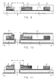
- FIGS. 1 to 8 of the annexed drawings show the principal manufacturing steps in FIGS. 1 to 8 of the annexed drawings and of a variant thereof whose principal manufacturing steps are illustrated in FIGS. 9 to 13 of the annexed drawings.
- FIG. 1A shows an example of a semi-finished product obtained by means of the not claimed manufacturing steps illustrated in FIGS. 1 to 4.
- FIG. 1A shows a flat substrate, e.g. of alumina or other material used as a substrate in thin film electronic technology on one face of which, called hereinafter front side, is seen a conductive path 2 interrupted by a resistive path 3 interconnected therewith.
- the conductive path 2 comprises also a pad 4 at the centre of which is seen a round area F' without metallization.
- FIG. 1A also shows an axis representing the outline of a cross section plane cutting perpendicularly the substrate 1 along the centre line of the round area F' and along a direction of the conductive path 2 and resistive path 3.
- the following figures 1 to 12 are without distinction referred to cross sections of the front or rear part of the substrate 1 in relation to said cross section plane. For drawing convenience the thicknesses of the elements shown there do not correspond to those of the true case. Furthermore for the same reason opposite the round area F' there is not shown everything which would be seen beyond the cross section plane.
- FIG. 1 refers to an initial step of the process during which on the front side of the substrate 1 are deposited three overlying metallic layers 5, 6 and 7 of standard thickness, using for the purpose one of the known methods of physical metal deposition, as for example is the deposition method for vacuum cathode sputtering of metals described in patent US-A-4226932 by means of which can be obtained the three metallic layers without interrupting the vacuum cycle.
- the innermost 5 adhering to the substrate 1 consists of resistive metal, e.g. tantalum or its compounds with nitrogen and oxygen.
- the intermediate layer 6 consists of adhesion metal, e.g. titanium.
- the outer layer 7 consists of a good conducting metal having antidiffusive behaviour such as for example palladium.
- the layer 5 taken alone constitutes the material of the resistive path 3 of FIG. 1A while taken together with layers 6 and 7 it contributes, after superposition of another layer of gold indicated by 9 in FIG. 2, to provision of the conductive path 2.
- layers 5, 6, 7 and 9 there can be used all those materials having analogous electrical and physical characteristics whose use is known in thin film technology.
- the outer layer 7 is first covered uniformly with an emulsion 8 photosensitive to ultraviolet radiation, hereinafter termed photoresist, and over which is applied a mask not shown in the figures and opaque to said radiation, in the areas of the paths 2, 3 and 4 excepting the area F'.
- photoresist photosensitive to ultraviolet radiation
- the mask to use should be opaque in the area complementary to the previous one.
- the photoresist 8 is exposed to ultraviolet light and then developed.
- the part of photoresist corresponding to said paths 2, 3 and 4, except the area F' is eliminated chemically during development.
- the metallic layer 7 free of photoresist 8 is grown galvanically a layer of gold 9 to complement the conductive path 2, which in this step is not yet differentiated from the resistive path 3.
- the residual photoresist after developing is removed chemically; after which the layers 5, 6 and 7 are removed from all the areas not covered by the layer of gold 9.
- lines wider than approximately 50(m removal takes place by chemical etching but otherwise by means of dry etching in plasma which does not require under-incision of the metallic lines and related detachment.
- what remains is only the conductive path 2 at the two sides of the area F' without metallization.
- the resistive path 3 by utilising the known art, i.e. deposition of photoresist, photomasking of the resistive path 3, development and selective chemical removal of the layers of gold 9, palladium 7 and titanium 6 above the layer of tantalum nitride 5 which constitutes the resistive path 3.
- the methods and reagents employed in the selective chemical etching of the layers 9, 6 and 7 are known to those skilled in the art.
- FIG. 5 shows a hole F obtained by means of known drilling systems using for example ultrasonic or laser drills.
- the cross section of the hole F can have a form other than circular and perfect verticality of the walls of the substrate 1 are not required to delimit the hole.
- the hole F does not cover the entire area F' and at the front side edge of the hole remains a circular corona of substrate 1 without metallization.
- FIG. 6 there follows a step of front & back deposition of a titanium layer 6' on which is overlain a palladium layer 7' and the thicknesses of the metallic layers 6' and 7' are standard.
- a step of front & back deposition of a titanium layer 6' on which is overlain a palladium layer 7' and the thicknesses of the metallic layers 6' and 7' are standard.
- the front & back cathodic depositions take place in two distinct vacuum cycles and this is a limit on the present technology of deposition equipment.
- the process which is the object of the present invention would not undergo however significant changes when in the future the limitation in this sense is made obsolete by the use of technologically more advanced equipment.
- the metallization obtained at the end of the deposition step appears uniform and covers without a break the following parts: the entire surface of the back side of the substrate 1, the wall delimiting the hole F in the body of the substrate 1, the area F' of the substrate 1 at the edge of the hole F, the entire surface of the front side of the substrate 1 where it overlies the conductive path 2 and the resistive path 3. Any chipped edges of the substrate 1 at the edges of the hole F are also covered uniformly by the deposited metals.
- the negative photoresist 10 is exposed by means of a mask, not shown in the figures, so that after development there remains uncovered a circular corona of palladium 7' with outside diameter D at the edge of the hole F.
- the layer of gold 11 covers the following parts: the entire back side surface, which thus is an excellent ground plane, the metallization of the interior of the hole F and on the edge F' as well as said circular corona of palladium 7' at the edge of the hole F. Thanks to the regularity and continuity of the layers 6' and 7' the layer of gold 11 also grows every place regularly and in particular inside and at the edges of the hole F.
- the photoresist 10 is eliminated entirely, after which is performed a selective chemical etching which removes the titanium layer 6' and palladium layer 7' from all the areas not covered by the gold layer 11.
- the methods and reagents employed in the selective chemical etching of the layers 6' and 7' are known to those skilled in the art.
- the desired product i.e. a substrate 1 comprising on the front side a conductive path consisting of the layers 9, 6 and 7 broken by a resistive path 3 and, through a metallized hole F, connected to a ground plane lying on the back side of the same substrate.
- the product obtained is a complete passive circuit for applications in the microwave field, or it constitutes part of a hybrid circuit which will be completed by known technologies of surface mounting and welding of chip devices in hybrid circuits.
- the front side can include only conductive or only resistive paths.
- the provision to be introduced is to arrange that at the point where the resistive path is to be connected to the ground plane on the back side, the masked area partially overlies the resistive path.
- Another generalisation is that of lengthening one or more conductive paths on the back side. In this case, again with reference to FIGS. 7 and 8, before galvanic growth of the layer of gold 11 there must be repeated also for the back side operations of photomasking analogous to those completed for the front side.
- the back side must be covered with a negative photoresist layer 10 on which are masked the areas affected by growth of back side conductive paths, not shown in the figures, at least one of these areas entirely overlying a hole F.
- a negative photoresist layer 10 on which are masked the areas affected by growth of back side conductive paths, not shown in the figures, at least one of these areas entirely overlying a hole F.
- the latter grows simultaneously on both sides in a single galvanic step.
- the residual photoresist 10 is eliminated all over and the final chemical etching removes the layers 6' and 7' in excess on the front side and back side.
- the excess layers are those deposited in areas which are outside the layer of gold 11 grown galvanically.
- FIG. 10 there follows a step of front & back deposition of a titanium layer 6'' on which is overlaid a palladium layer 7'', the thicknesses of the metallic layers 6'' and 7'' are standard. Even in this case it is convenient to use the deposition technique described in the above mentioned patent US-A-4226932. If it is desired to use other vacuum deposition techniques for the metals it is necessary to choose those in which heating of the substrate 1 is not called for, to avoid alterations of the photoresist 10'. Before the metallization it is also advisable to apply on the front side of the substrate 1 a peripheral corona, not shown in the figures, which would prevent deposition of metal along the contour of the substrate for reasons explained below.
- the metallization obtained at the end of the deposition step appears uniform and covers without a break the following parts: the entire back side surface, the wall delimiting the hole F in the body of the substrate 1, the area F' free of metal at the edge of the hole F, the circular corona free of photoresist on the layer of gold 9, and lastly the entire surface of the photoresist 10' on the front side. Any chipped edges of the substrate 1 at the edges of the hole F are covered uniformly by the deposited metals.
- the off-lifted photoresist entrains with it the overlying metallization 6'' and 7''.
- the lift-off operation is done by immersing the substrate for a predetermined time in a thermostatically controlled bath containing a chemical solution of known composition (stripper) depending on the type of photoresist used.
- the solution agitated continuously by means of ultrasonics, begins to lift off the photoresist 10' starting from the edges of the substrate which, due to the above peripheral protection, are unmetallized.
- the stripping action moves towards the interior until all the photoresist 10' and the overlying metals are removed from the substrate 1.
- the latter cover the following parts: the entire back side surface of the substrate 1, the wall delimiting the hole F, the area F' of the substrate 1, and lastly the circular corona of gold 9 at the edge of the hole F.
- a layer of gold 11 having standard thickness is grown galvanically.
- the layer of gold 11 covers the following parts: the entire back side surface, which thus constitutes an excellent ground plane, metallization inside the hole F and on the edge F', as well as a circular corona of palladium 7'' at the edge of the hole F. Thanks to the regularity and continuity of the layer 6'' and 7'', even the layer of gold 11 grows everywhere regularly and in particular inside and at the edges of the hole F. To obtain the final product, coinciding with that shown in FIG 13, it is sufficient to eliminate the residual photoresist 10'.
- the process in accordance with the variant has more generalised use applicable both for the wide conductive lines and the fine lines. But it is technologically more complex than the main process because it includes the photoresist lift-off operation whose performance calls for good technical and practical skill. Therefore, when the width of the conductive paths is not less than approximately 50 ⁇ m the main process is preferable.
Landscapes
- Engineering & Computer Science (AREA)
- Microelectronics & Electronic Packaging (AREA)
- Manufacturing & Machinery (AREA)
- Apparatuses And Processes For Manufacturing Resistors (AREA)
- Manufacturing Of Printed Wiring (AREA)
- Parts Printed On Printed Circuit Boards (AREA)
Claims (13)
- Verfahren zur Herstellung von metallischen Löchern in einem dielektrischen Substrat (1) mit Vorder- und Rückseite und Leiter- und/oder Widerstandsbahnen (2, 3) überzogen mit metallischen Schichten (5, 6, 7) auf der Vorderseite des Substrats, dadurch gekennzeichnet, daß es aufeinanderfolgend die folgenden Schritte umfaßt:a) Bohren des genannten Substrats (1) in Zonen, die frei von Metallauftragungen der genannten Leiter- (2) und/oder Widerstandbahnen (3) sind,b) sorgfältiges Reinigen der genannten Vorder- und Rückseite des dielektrischen Substrats (1) und der Wände, die die Löcher (F) im Körper des Substrats begrenzen,c) Aufdampfen im Vakuum von Metallen (6', 7') auf die genannten Vorder- und Rückseiten und auf den Wänden der Löcher (F), wobei eine elektrische Kontinuität zwischen der Vorder- und Rückseite des dielektrischen Substrats (1) durch die Löcher erreicht wird,d) Überziehen der Vorderseite mit einer Schicht einer negativen photosensiblen Emulsion (10), die nachstehend Photoresist genannt wird, und Abdeckung von Zonen (D), die die Löcher (F) vollkommen überlagern und teilweise die genannten Leiter- (2) und/oder Widerstandsbahnen (3) überlagern, Exposition und Entwicklung, wodurch man unbedeckte kreisförmige Zonen (D) um die Rändern der Löcher (F) an der Vorderseite erhält,e) galvanische Zunahme von Metall (11) über die genannten unbedeckten, kreisförmigen Zonen (D) an der Vorderseite um die Ränder der Löcher (F), auf den genannten Wänden, die die Löcher im Körper des Substrats begrenzen, und auf der ganzen Oberfläche der Rückseite, wodurch eine Grundlage geschaffen wird.,f) Entfernung des restlichen Photoresists (10) von der Vorderseite, undg) Entfernung der genannten pulverisierten Metalle (6', 7'), die unbedeckt vom genannten galvanisch zugenommenen Metall (11) verblieben sind, von der Vorderseite.
- Verfahren zur Hersteilung metallisierten Durchgangslöchern in einem dielektrischen Sustrat (1) mit Vorder- und Rückseiten und Leiter- und/oder Widerstandsbahnen (2, 3) überdeckt mit metallischen Schichten (5, 6, 7) auf der Vorderseite des Substrats, dadurch gekennzeichnet, daß es aufeinanderfolgend folgende Schritte umfaßt:a1) Bohren des genannten Substrats (1) in Zonen, die frei von Metallisierung der genannten Leiter- (2) und/oder Widerstandsbahnen (3) sind,b1) sorgfältiges Reinigen der Vorder- und Rückseite des dielektrischen Substrats (1) und der Wände, die die Löcher (F) im Körper des Substrats begrenzen,c1) Aufdampfen im Vakuum von Metallen (6', 7') auf den genannten Vorder- und Rückseiten und auf den Wänden der Löcher (F), wodurch eine elektrische Kontinuität zwischen der Vorder- und Rückseite des dielektrischen Substrats (1) durch die Löcher erreicht wird,d1) Überziehen der Vorderseite mit einer Schicht einer negativ photosensiblen Emulsion (10'), nachstehend Photoresist genannt, und Abdeckung von Zonen (D), die vollkommen die Löcher (F) und teilweise die genannten Leiter (2) und/oder Widerstandsbahnen (3) überdecken, Exposition und Entwicklung des abgedeckten Photoresist und, wodurch man unbedeckte, kreisförmige Zonen (D) um die Ränder auf der Vorderseite der Löcher (F) erhält,d2) Überziehen der Rückseite mit einer Schicht einer negativen Photoresists und Abdecken von Zonen, auf deren Rückseite Leiterbahnen sich ausbreiten sollen, wobei wenigstens eine der genannten abgedeckten Zonen (D) ein Loch (F) vollkommen überdeckt, Exposition und Entwicklung der abgedeckten Photoresists, wodurch man unbedeckte Rückseitenzonen erhält,e1) galvanische Zunahme von Metall (11) über die genannten Zonen (D) der Vorder- und Rückseite und auf den Wänden, die die Löcher im Körper des Substrats begrenzen,f1) Entfernung des restlichen Photoresists (10') von der Vorder- und Rückseite, undg1) Entfernung der genannten pulverisierten Metalle (6', 7') von der Vorder- und Rückseite, die nicht durch das galvanisch ausgebreitete Metall (11) bedeckt werden.
- Verfahren zur Herstellung von metallisierten Löchern in einem dielektrischen Substrat mit Leiter- und/oder Widerstandsbahnen entsprechend Anspruch 1 oder 2, dadurch gekennzeichnet, daß die genannten, im Vakuum aufgedampften Metalle sich so setzen, daß sie eine Haftbeschichtung (6') bilden, die von einer leitenden, metallischen Schicht mit antidiffusiven Eigenschaften (7') überdeckt wird.
- Verfahren zur Herstellung von metallisierten Löchern in einem dielektrischen Substrat mit Leiter- und/oder Widerstandsbahnen entsprechend Anspruch 3, dadurch gekennzeichnet, daß die genannte Haftschicht (6') aus Titan und die genannte leitende, metallische Schicht aus Palladium besteht.
- Verfahren zur Herstellung von metallisierten Löchern in einem dielektrischen Substrat mit Leiter- und/oder Widerstandsbahnen entsprechend Anspruch 1 oder 2, dadurch gekennzeichnet, daß das galvanisch ausgebreitete Metall (11) Gold ist.
- Verfahren zur Herstellung von metallisierten Löchern in einem dielektrischen Substrat mit Leiter- und/oder Widerstandbahnen entsprechend Anspruch 1 oder 2, dadurch gekennzeichnet, daß es sich bei dem genannten Schritt g) oder g1) betreffs der Entfernung der genannten Metalle (6', 7') um selektives chemisches Ätzen handelt.
- Verfahren zur Herstellung von metallisierten Löchern in einem dielektrischen Substrat (1) mit Vorder- und Rückseiten und Leiter- und/oder Widerstandsbahnen (2, 3) die mit metallischen Schichten (5, 6, 7) auf der Vorderseite des Substrats bedeckt sind, dadurch gekennzeichnet, daß es aufeinanderfolgend folgende Schritte umfaßt:l) Bohren des genannten Substrats (1) in Zonen, die frei von Metallisierungen der genannten Leiter- (2) und/oder Widerstandsbahnen (3) sind,m) sorgfältiges Reinigender genannten Vorder- und Rückseite des dielektrischen Substrats (1) und der Wände, die die Löcher (F) im Körper des Substrats begrenzen,n) Überziehen der Vorderseite mit einer Schicht einer negativ photosensiblen Emulsion (10'), nachstehend Photoresist genannt, und Abdeckung von Zonen (D), die die Löcher (F) vollkommen und teilweise die genannten Leiter- (2) und/oder Widerstandsbahnen (3) überdecken, Exposition und Entwicklung von abgedeckten Photoresists, wodurch man nicht abgedeckte, kreisförmige Zonen (D) des nackten Substrats (1) an den Rändern der Löcher (F) auf der Vorderseite erhält,o) sorgfältiges Reinigen der genanten nackten Zonen (D) an den Rändern der Löcher (F) und in ihnen,p) Aufdampfen im Vakuum von Metallen (6', 7') über den restlichen Photoresist auf der Vorderseite, auf den genannten kreisförmigen Zonen (D) des nackten Substrats an den Rändern der Löcher, auf den Wänden, die die Löcher (F) im Körper des Substrats begrenzen, und auf der gesamten Oberfläche der Rückseite, wodurch man eine elektrische Kontinuität zwischen der Vorder- und der Rückseite des dielektrischen Substrats (1) durch die Löcher erhält,q) Entfernung des restlichen Photoresists (10') und der Metalle (6", 7"), die ihn von der genannten Vorderseite überdecken,r) Überdecken der Vorderseite mit einer Schicht eines negativen Photoresists (10') und Abdecken von Zonen, die die Löcher (F) vollkommen und teilweise die genannten Leiter- (2) und Widerstandsbahnen (3) abdecken, Exposition und Entwicklung des abgedeckten Photoresists, wodurch man unbedeckte, kreisförmige Zonen (D) der genannten aufgedampften Metalle (6", 7"), die nach der Abnahme an den Rändern der Löcher an der Vorderseite verbleiben,s) galvanisches Ausbreiten von Metall (11) über die genannten unbedeckten, kreisförmigen Zonen (D) der verbleibenden aufgedampften Metalle (6", 7"), auf den genannten Wänden, die die Löcher im Körper des Substrats begrenzen. und auf der gesamten Oberfläche der Rückseite, wodurch eine Grundlage geschaffen wird, undt) Entfernung des genannte restlichen Photoresists (10') von der Vorderseite.
- Verfahren zur Herstellung von metallisierten durchgehenden Löchern in einem dielektrischen Substrat (1) mit Vorder- und Rückseiten und Leiter- (2) und/oder Widerstandsbahnen (3) überdeckt mit metallischen Schichten (5, 6, 7) auf der Vorderseite des Substrats, dadurch gekennzeichnet, daß es aufeinanderfolgend folgende Schritte umfaßt:l1) Bohren des genannten Substrats (1) in Zonen, die frei von Metallisierungen der genannten Leiter- (2) und/oder Widerstandsbahnen (3) sind,m1) Sorgfältiges Reinigen der genannten Vorder- und Rückseite des dielektrischen Substrats (1) und der Wände, die die Löcher (F) im Körper des Substrats begrenzen,n1) Überziehen der Vorderseite mit einer Schicht aus einer negativ photosensiblen Emulsion (10'), nachfolgend Photoresist genannt, und Abdeckung von Zonen (D) die die Löcher (F) vollkommen und die genannten Leiter- (2) und Widerstandsbahnen (3) teilweise überdecken, Exposition und Entwicklung des abgedeckten Photoresists, wodurch man unbedeckte, kreisförmige Zonen (D) des nackten Substrats (1) an der Vorderseite an den Rändern der Löcher (F) erhält,o1) Sorgfältiges Reinigen der nackten Zonen (D) an den Rändern der Löcher (F) und in ihnen,p1) Aufdampfen im Vakuum von Metallen (6", 7") über dem vorderseitigen, restlichen Photoresist (10'), auf den genannten kreisförmigen Zonen (D) des nackten Substrats an den Rändern der Löcher, auf den genannten Wänden, die die Löcher (F) im Körper des Substrats begrenzen, und auf der gesamten rückseitigen Oberfläche, wodurch man eine elektrische Kontinuität zwischen der Vorder- und der Rückseite des dielektrischen Substrats (1) durch die Löcher erhält,q1) Abnahme des genannten restlichen Photoresists (10') und der diesen abdeckenden Metalle (6", 7") von der genannten Vorderseite,r1) Überdecken der Vorderseite mit einer Schicht aus einem negativen Photoresist (10') und Abdeckung von Zonen (D), die die Löcher (F) vollkommen und die genannten Leiter- (2) und/oder Widerstandsbahnen (3) teilweise abdecken, Exposition und Entwicklung des abgedeckten Photoresists, wodurch man unbedeckte, kreisförmige Zonen (D) der genannten aufgedampften Metalle (6", 7"), die nach der Abnahme an den vorderseitigen Rädern der Löcher verbleiben,r2) Abdecken der Rückseite mit einer Schicht eines negativen Photoresists und Abdecken von Zonen, auf der rückseitige Leiterbahnen verwirklicht werden sollen, wobei mindestens eine genannte abgedeckte Zone (D) ein Loch (F) vollkommen abdeckt, Exposition und Entwicklung des abgedeckten Photoresists, wodurch man unbedeckte rückseitige Zonen erhält,s1) galvanisches Ausbreiten von Metall (11) über die genannten unbedeckten vorder- und rückseitigen Zonen (D) und auf den Wänden, die die Löcher im Körper des Substrats begrenzen,t1) Entfernung des restlichen Photoresists (10') von der Vorder- und Rückseite,u) Überdecken der Vorderseite mit einer gleichförmigen Schicht eines schützenden, organischen Materials,v) Entfernung der genannten aufgedampften Metalle (6", 7"), die nicht durch das genannte, galvanisch auf der Rückseite ausgebreitete Metall (11) überdeckt sind, wodurch man rückseitige Leiterbahnen erhält,z) Entfernung des genannten schützenden organischen Materials von der Vorderseite.
- Verfahren zur Herstellung von metallisierten Löchern in einem dielektrischen Substrat mit Leiter- und/oder Widerstandsbahnen entsprechend Anspruch 7 oder 8, dadurch gekennzeichnet, daß das genannte in Schritt m) oder m1) ausgeführte sorgfältige Reinigen auf chemischem Wege ausgeführt wird und daß das in Schritt o) oder o1) ausgeführte sorgfältige Reinigen durch Anwendung eines geeigneten Plasmagases durchgeführt wird.
- Verfahren zur Herstellung von metallisierten Löchern in einem dielektrischen Substrat mit Leiter und/oder Widerstandsbahnen entsprechend Anspruch 7 oder 8, dadurch gekennzeichnet, daß die genannten aufgedampften Metalle sich so ablagern, daß sie eine Haftschicht (6") bilden, die von einer metallischen Leitschicht mit antidiffusiven Eigenschaften (7") überlagert wird
- Verfahren zur Herstellung von metallisierten Löchern in einem dielektrischen Substrat mit Leiter- und/oder Widerstandsbahnen entsprechend Anspruch 10, dadurch gekennzeichnet, daß die genannte Haftschicht (6") aus Titan und die genannte metallische Leitschicht mit antidiffusiven Eigenschaften (7") aus Palladium besteht.
- Verfahren zur Herstellung von metallisierten Löchern in einem dielektrischen Substrat mit Leiter- und/oder Widerstandsbahnen entsprechend Anspruch 7 oder 8, dadurch gekennzeichnet, daß das genannte galvanisch ausgebreitete Metall (11) Gold ist.
- Verfahren zur Herstellung von metallisierten Löchern in einem dielektrischen Substrat mit Leiter- und/oder Widerstandsbahnen entsprechend Anspruch 8, dadurch gekennzeichnet, daß der genannte Schritt v) betreffs der Entfernung des genannten Metalle (6", 7") ein selektiver chemischer Ätzungsverfahren ist.
Applications Claiming Priority (4)
| Application Number | Priority Date | Filing Date | Title |
|---|---|---|---|
| ITMI932697 | 1993-12-22 | ||
| ITMI932698 | 1993-12-22 | ||
| IT93MI002698A IT1265415B1 (it) | 1993-12-22 | 1993-12-22 | Processo per la realizzazione di fori metallizzati in substrati dielettrici comprendenti percorsi conduttivi e/o resistivi in film |
| IT93MI002697A IT1265414B1 (it) | 1993-12-22 | 1993-12-22 | Processo per la realizzazione di fori metallizzati in substrati dielettrici comprendenti percorsi conduttivi e/o resistivi in film |
Publications (2)
| Publication Number | Publication Date |
|---|---|
| EP0670668A1 EP0670668A1 (de) | 1995-09-06 |
| EP0670668B1 true EP0670668B1 (de) | 1998-01-28 |
Family
ID=26331076
Family Applications (1)
| Application Number | Title | Priority Date | Filing Date |
|---|---|---|---|
| EP94117039A Expired - Lifetime EP0670668B1 (de) | 1993-12-22 | 1994-10-27 | Verfahren zur Herstellung von metallisierten Löchern in dielektrischen Substraten mit untereinander verbundenen Dünnschichtleiter- und/oder Widerstandsbahnen |
Country Status (3)
| Country | Link |
|---|---|
| EP (1) | EP0670668B1 (de) |
| AT (1) | ATE162924T1 (de) |
| DE (1) | DE69408298D1 (de) |
Cited By (1)
| Publication number | Priority date | Publication date | Assignee | Title |
|---|---|---|---|---|
| EP1111679A3 (de) * | 1999-12-21 | 2008-01-02 | Philips Intellectual Property & Standards GmbH | Bauteil mit Dünnschichtschaltkreis |
Families Citing this family (4)
| Publication number | Priority date | Publication date | Assignee | Title |
|---|---|---|---|---|
| IT1279080B1 (it) * | 1995-11-29 | 1997-12-04 | Sits Soc It Telecom Siemens | Processo di fabbricazione di circuiti in film sottile comprendenti condensatori integrati |
| CN102946691B (zh) * | 2012-11-07 | 2015-04-29 | 东莞生益电子有限公司 | 含局部金属化的台阶开槽的pcb板制作方法 |
| CN105578801B (zh) * | 2015-12-15 | 2018-04-03 | 深圳崇达多层线路板有限公司 | 一种阻焊油墨半塞孔的背钻孔的制作方法 |
| CN119450903B (zh) * | 2023-08-03 | 2025-11-14 | 庆鼎精密电子(淮安)有限公司 | 具有金属化半孔的电路板及其制备方法 |
Family Cites Families (5)
| Publication number | Priority date | Publication date | Assignee | Title |
|---|---|---|---|---|
| US4226932A (en) * | 1979-07-05 | 1980-10-07 | Gte Automatic Electric Laboratories Incorporated | Titanium nitride as one layer of a multi-layered coating intended to be etched |
| US4402998A (en) * | 1982-01-04 | 1983-09-06 | Western Electric Co., Inc. | Method for providing an adherent electroless metal coating on an epoxy surface |
| DE3524832A1 (de) * | 1985-07-11 | 1987-01-15 | Siemens Ag | Herstellung von duennfilmschaltungen |
| IT1191680B (it) * | 1986-03-19 | 1988-03-23 | Gte Telecom Spa | Processo per la realizzazione di fori metallizzati in un substrato dotato di cammini conduttivi e resistivi,e prodotto ottenuto con il processo suddetto |
| IT1216135B (it) * | 1988-03-18 | 1990-02-22 | Sits Soc It Telecom Siemens | Dielettrico mediante deposizioni in processo per la realizzazione di vuoto di metalli, e relativo fori metallizzati in un substrato prodotto ottenuto. |
-
1994
- 1994-10-27 DE DE69408298T patent/DE69408298D1/de not_active Expired - Lifetime
- 1994-10-27 EP EP94117039A patent/EP0670668B1/de not_active Expired - Lifetime
- 1994-10-27 AT AT94117039T patent/ATE162924T1/de not_active IP Right Cessation
Cited By (1)
| Publication number | Priority date | Publication date | Assignee | Title |
|---|---|---|---|---|
| EP1111679A3 (de) * | 1999-12-21 | 2008-01-02 | Philips Intellectual Property & Standards GmbH | Bauteil mit Dünnschichtschaltkreis |
Also Published As
| Publication number | Publication date |
|---|---|
| ATE162924T1 (de) | 1998-02-15 |
| DE69408298D1 (de) | 1998-03-05 |
| EP0670668A1 (de) | 1995-09-06 |
Similar Documents
| Publication | Publication Date | Title |
|---|---|---|
| US4272561A (en) | Hybrid process for SBD metallurgies | |
| CA1301952C (en) | Selective solder formation on printed circuit boards | |
| JPS5812344B2 (ja) | 銅を基材とする金属パタ−ンの形成方法 | |
| EP0670668B1 (de) | Verfahren zur Herstellung von metallisierten Löchern in dielektrischen Substraten mit untereinander verbundenen Dünnschichtleiter- und/oder Widerstandsbahnen | |
| JPH0987828A (ja) | 電子部品の電極を形成する方法およびそれに用いる装置 | |
| US5011761A (en) | Process for making metallized holes in a dielectric substrate by vacuum deposition of metals and the product obtained thereby | |
| EP0112898A1 (de) | Herstellung schweissbarer platten für integrierte schaltungen | |
| US5979048A (en) | Method of manufacturing connectors | |
| JPS59215790A (ja) | 印刷回路板の製造法 | |
| US3649392A (en) | Thin-film circuit formation | |
| US4011144A (en) | Methods of forming metallization patterns on beam lead semiconductor devices | |
| US5403466A (en) | Silver plating process for lead frames | |
| US3421206A (en) | Method of forming leads on semiconductor devices | |
| US5023994A (en) | Method of manufacturing a microwave intergrated circuit substrate including metal lined via holes | |
| JPH05259615A (ja) | 回路導体の形成方法 | |
| US4157284A (en) | Process to obtain conductive and resistive elements in microwave microcircuits | |
| JPH07254534A (ja) | 電子部品の外部電極形成方法 | |
| ITMI932697A1 (it) | Processo per la realizzazione di fori metallizzati in substrati dielettrici comprendenti percorsi conduttivi e/o resistivi in film sottile tra di loro interconnessi | |
| JP3704196B2 (ja) | セラミック配線板の形成方法 | |
| JPS6235361A (ja) | フオトマスク材料 | |
| ITMI932698A1 (it) | Processo per la realizzazione di fori metallizzati in substrati dielettrici comprendenti percorsi conduttivi e/o resistivi in film sottile, in particolare per linee fini | |
| Aramati et al. | Thin-film microwave integrated circuits | |
| JP3077520B2 (ja) | 電子素子の電極形成方法 | |
| JPS5856422A (ja) | パタ−ン形成法 | |
| JPH05308182A (ja) | 膜回路基板の製造方法 |
Legal Events
| Date | Code | Title | Description |
|---|---|---|---|
| PUAI | Public reference made under article 153(3) epc to a published international application that has entered the european phase |
Free format text: ORIGINAL CODE: 0009012 |
|
| AK | Designated contracting states |
Kind code of ref document: A1 Designated state(s): AT BE CH DE DK ES FR GB GR IT LI NL SE |
|
| 17P | Request for examination filed |
Effective date: 19960104 |
|
| 17Q | First examination report despatched |
Effective date: 19960320 |
|
| RAP1 | Party data changed (applicant data changed or rights of an application transferred) |
Owner name: ITALTEL S.P.A. |
|
| GRAG | Despatch of communication of intention to grant |
Free format text: ORIGINAL CODE: EPIDOS AGRA |
|
| GRAG | Despatch of communication of intention to grant |
Free format text: ORIGINAL CODE: EPIDOS AGRA |
|
| GRAH | Despatch of communication of intention to grant a patent |
Free format text: ORIGINAL CODE: EPIDOS IGRA |
|
| GRAH | Despatch of communication of intention to grant a patent |
Free format text: ORIGINAL CODE: EPIDOS IGRA |
|
| GRAA | (expected) grant |
Free format text: ORIGINAL CODE: 0009210 |
|
| AK | Designated contracting states |
Kind code of ref document: B1 Designated state(s): AT BE CH DE DK ES FR GB GR IT LI NL SE |
|
| PG25 | Lapsed in a contracting state [announced via postgrant information from national office to epo] |
Ref country code: NL Free format text: LAPSE BECAUSE OF FAILURE TO SUBMIT A TRANSLATION OF THE DESCRIPTION OR TO PAY THE FEE WITHIN THE PRESCRIBED TIME-LIMIT Effective date: 19980128 Ref country code: LI Free format text: LAPSE BECAUSE OF FAILURE TO SUBMIT A TRANSLATION OF THE DESCRIPTION OR TO PAY THE FEE WITHIN THE PRESCRIBED TIME-LIMIT Effective date: 19980128 Ref country code: IT Free format text: LAPSE BECAUSE OF FAILURE TO SUBMIT A TRANSLATION OF THE DESCRIPTION OR TO PAY THE FEE WITHIN THE PRE;WARNING: LAPSES OF ITALIAN PATENTS WITH EFFECTIVE DATE BEFORE 2007 MAY HAVE OCCURRED AT ANY TIME BEFORE 2007. THE CORRECT EFFECTIVE DATE MAY BE DIFFERENT FROM THE ONE RECORDED.SCRIBED TIME-LIMIT Effective date: 19980128 Ref country code: GR Free format text: LAPSE BECAUSE OF FAILURE TO SUBMIT A TRANSLATION OF THE DESCRIPTION OR TO PAY THE FEE WITHIN THE PRESCRIBED TIME-LIMIT Effective date: 19980128 Ref country code: FR Free format text: LAPSE BECAUSE OF FAILURE TO SUBMIT A TRANSLATION OF THE DESCRIPTION OR TO PAY THE FEE WITHIN THE PRESCRIBED TIME-LIMIT Effective date: 19980128 Ref country code: ES Free format text: THE PATENT HAS BEEN ANNULLED BY A DECISION OF A NATIONAL AUTHORITY Effective date: 19980128 Ref country code: CH Free format text: LAPSE BECAUSE OF FAILURE TO SUBMIT A TRANSLATION OF THE DESCRIPTION OR TO PAY THE FEE WITHIN THE PRESCRIBED TIME-LIMIT Effective date: 19980128 Ref country code: BE Free format text: LAPSE BECAUSE OF FAILURE TO SUBMIT A TRANSLATION OF THE DESCRIPTION OR TO PAY THE FEE WITHIN THE PRESCRIBED TIME-LIMIT Effective date: 19980128 Ref country code: AT Free format text: LAPSE BECAUSE OF FAILURE TO SUBMIT A TRANSLATION OF THE DESCRIPTION OR TO PAY THE FEE WITHIN THE PRESCRIBED TIME-LIMIT Effective date: 19980128 |
|
| REF | Corresponds to: |
Ref document number: 162924 Country of ref document: AT Date of ref document: 19980215 Kind code of ref document: T |
|
| REG | Reference to a national code |
Ref country code: CH Ref legal event code: EP |
|
| REF | Corresponds to: |
Ref document number: 69408298 Country of ref document: DE Date of ref document: 19980305 |
|
| PG25 | Lapsed in a contracting state [announced via postgrant information from national office to epo] |
Ref country code: SE Free format text: LAPSE BECAUSE OF FAILURE TO SUBMIT A TRANSLATION OF THE DESCRIPTION OR TO PAY THE FEE WITHIN THE PRESCRIBED TIME-LIMIT Effective date: 19980428 Ref country code: DK Free format text: LAPSE BECAUSE OF FAILURE TO SUBMIT A TRANSLATION OF THE DESCRIPTION OR TO PAY THE FEE WITHIN THE PRESCRIBED TIME-LIMIT Effective date: 19980428 |
|
| PG25 | Lapsed in a contracting state [announced via postgrant information from national office to epo] |
Ref country code: DE Free format text: LAPSE BECAUSE OF FAILURE TO SUBMIT A TRANSLATION OF THE DESCRIPTION OR TO PAY THE FEE WITHIN THE PRESCRIBED TIME-LIMIT Effective date: 19980429 |
|
| EN | Fr: translation not filed | ||
| NLV1 | Nl: lapsed or annulled due to failure to fulfill the requirements of art. 29p and 29m of the patents act | ||
| REG | Reference to a national code |
Ref country code: CH Ref legal event code: PL |
|
| PG25 | Lapsed in a contracting state [announced via postgrant information from national office to epo] |
Ref country code: GB Free format text: LAPSE BECAUSE OF NON-PAYMENT OF DUE FEES Effective date: 19981027 |
|
| PLBE | No opposition filed within time limit |
Free format text: ORIGINAL CODE: 0009261 |
|
| STAA | Information on the status of an ep patent application or granted ep patent |
Free format text: STATUS: NO OPPOSITION FILED WITHIN TIME LIMIT |
|
| 26N | No opposition filed | ||
| GBPC | Gb: european patent ceased through non-payment of renewal fee |
Effective date: 19981027 |