EP0668584B1 - Procédé de fabrication d'un disque maítre ou d' un disque optique - Google Patents
Procédé de fabrication d'un disque maítre ou d' un disque optique Download PDFInfo
- Publication number
- EP0668584B1 EP0668584B1 EP95400351A EP95400351A EP0668584B1 EP 0668584 B1 EP0668584 B1 EP 0668584B1 EP 95400351 A EP95400351 A EP 95400351A EP 95400351 A EP95400351 A EP 95400351A EP 0668584 B1 EP0668584 B1 EP 0668584B1
- Authority
- EP
- European Patent Office
- Prior art keywords
- layer
- succession
- micropits
- resin
- microcuvettes
- Prior art date
- Legal status (The legal status is an assumption and is not a legal conclusion. Google has not performed a legal analysis and makes no representation as to the accuracy of the status listed.)
- Expired - Lifetime
Links
Images
Classifications
-
- G—PHYSICS
- G11—INFORMATION STORAGE
- G11B—INFORMATION STORAGE BASED ON RELATIVE MOVEMENT BETWEEN RECORD CARRIER AND TRANSDUCER
- G11B7/00—Recording or reproducing by optical means, e.g. recording using a thermal beam of optical radiation by modifying optical properties or the physical structure, reproducing using an optical beam at lower power by sensing optical properties; Record carriers therefor
- G11B7/24—Record carriers characterised by shape, structure or physical properties, or by the selection of the material
- G11B7/26—Apparatus or processes specially adapted for the manufacture of record carriers
- G11B7/263—Preparing and using a stamper, e.g. pressing or injection molding substrates
-
- Y—GENERAL TAGGING OF NEW TECHNOLOGICAL DEVELOPMENTS; GENERAL TAGGING OF CROSS-SECTIONAL TECHNOLOGIES SPANNING OVER SEVERAL SECTIONS OF THE IPC; TECHNICAL SUBJECTS COVERED BY FORMER USPC CROSS-REFERENCE ART COLLECTIONS [XRACs] AND DIGESTS
- Y10—TECHNICAL SUBJECTS COVERED BY FORMER USPC
- Y10S—TECHNICAL SUBJECTS COVERED BY FORMER USPC CROSS-REFERENCE ART COLLECTIONS [XRACs] AND DIGESTS
- Y10S430/00—Radiation imagery chemistry: process, composition, or product thereof
- Y10S430/146—Laser beam
Definitions
- the present invention relates to a process of manufacture of a master disc and / or a disc optical.
- WORM type optical discs consist of a preformatted substrate, usually polycarbonate, covered with one or more sensitive layers which change on contact with a beam emitted by a laser diode by ablating microcuvettes representative of the information to be recorded.
- This pre-engraving can integrate a time base, suitable to allow the speed of rotation to be controlled of the substrate, this time base being constituted either by a wobbulation in the continuous groove, i.e. from formats already specified in particular in international standards (sampled format or continuous composite).
- the master discs, the pressing dies and therefore optical discs obtained include not only the information to duplicate and / or read but also the signal of preformatting, which disturbs the reading of information.
- the invention aims to overcome this drawback by proposing a preformatted substrate usable for manufacturing of optical discs and for manufacturing master discs allowing the manufacture of dies usable for pressing discs optics.
- a layer of hard material is deposited, reflective in the near infrared and conductive on the succession of microcuvettes formed in the support.
- a preformatted substrate comprising information and methods of manufacturing a master disc or a optical disc of the invention
- recording of information is done in the resin areas located under the first succession of microcuvettes or first groove.
- the recording of information is carried out in resin zones different from those located under the first succession of microcuvettes or first furrow.
- the thickness of the resin layer sensitive to at least one stress is between approximately 100 nm and approximately 1 ⁇ m, and the depth of the first succession of microcuvettes or first groove is approximately 75 nm.
- the support is glass.
- the support is aluminum.
- the support is made of a hard material, reflecting in the near infrared and conductive.
- the support is not made of a hard material, reflecting in the near infrared and conducting
- the transfer of information will then be done in this layer of hard material, reflecting in the near infrared and conductive.
- the hard material, reflective in the near infrared and conductive is chosen from a nitride or carbonitride of zirconium, hafnium or titanium.
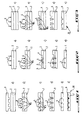
- FIG. 1 schematically illustrates a first mode of implementation of the disc manufacturing process master and / or an optical disc of the invention.
- Figure 2 schematically illustrates a second mode of implementation of the disc manufacturing process master and / or an optical disc of the invention.
- Figure 3 schematically illustrates a third mode of implementation of the disc manufacturing process master and / or an optical disc of the invention.
- the preformatted substrates of the invention are consist of a support with smooth surfaces, that is to say having no roughness greater than 50 ⁇ , of which one side is covered with a layer of resin sensitive to at least one constraint, this layer of resin comprising a first succession of microcuvettes or first groove whose depth is less than the thickness of the resin layer sensitive.
- the support will consisting of tempered and / or dealkalized glass. I1 may also be made of aluminum. He will be able to still be made of a hard, reflective material in the near infrared and conductive. In the cases where the support is not made of hard material, reflecting in the near infrared and conducting, the preformatted substrate of the invention may, in addition, between the sensitive resin layer and the support a layer of such a material.
- This material will be more particularly chosen from a nitride or carbonitride of zirconium, hafnium or titanium.
- first succession of microcuvettes or first groove representative of the preformatting signal
- sentence "first succession of microcuvettes or first groove "as used here means that the preformatting signal can also be well in the form of a succession of microcuvettes that of a continuous groove, different means can be employees.
- a first way consists in applying a matrix of pressing on the sensitive resin layer, this pressing die comprising microreliefs representative in negative of the preformatting signal. By pressing this matrix into the resin layer sensitive, we will directly obtain the first succession of microcuvettes or first furrow desired.
- the first succession of microcuvettes or first groove can still be created by irradiation of certain areas of the sensitive resin layer, for example scrolling of a light beam, for example emitted by a laser source, modulated according to the signal preformat. Again, the exposed areas of resin will then be eliminated, by chemical attack, on a depth less than the thickness of the layer of sensitive resin.
- the thickness of the sensitive resin layer is between about 100 nm and about 1 ⁇ m and the depth of microcuvettes of the first succession of microcuvettes or the first groove is about 75 nm.
- the preformatted substrates of the invention are then usable for recording information in all types of recorders requiring a substrate preformatted. More particularly, a WORM type recorder for recording information.
- the information may be saved in the remaining resin areas located under the first succession of microcuvettes or in zones different from these.
- this irradiation will be done for example with radiation at low energy so as not to desensitize the resin located under this first succession of microcuvettes or first furrow.
- Information can be saved, as in the case of the preformatting signal, by pressing a matrix comprising representative microreliefs in negative information to record and duplicate, or by irradiation through a mask containing the information to be recorded and duplicate followed by a step of elimination by attack chemical of the resin areas thus irradiated or by the movement of a light beam modulated in signal function to record and duplicate tracking also a step of eliminating the resin zones insolated.
- a matrix comprising representative microreliefs in negative information to record and duplicate
- irradiation through a mask containing the information to be recorded and duplicate followed by a step of elimination by attack chemical of the resin areas thus irradiated or by the movement of a light beam modulated in signal function to record and duplicate tracking also a step of eliminating the resin zones insolated.
- the depth of the microcuvettes constituting this second succession of microcuvettes must be equal to the thickness of the sensitive resin layer in which they are created.
- the substrate preformatted with information to duplicate from the invention will consist of a support covered with a photosensitive resin layer comprising a first succession of microcuvettes or first furrow whose depth is less than the thickness of the layer of sensitive resin and a second succession of microcuvettes whose depth is equal to the thickness of the sensitive layer in areas where they are created.
- the depth microcuvettes of the second succession of microcuvettes representative of the information to be duplicate, will go to the surface of the support.
- the support can consist of all the materials listed above for the material preformatted previously described. And, when the support is not made of hard material, reflecting in the near infrared but covered with a layer of this material, the depth of the microcuvettes of the second succession of microcuvettes will go up to the surface of this material.
- Preformatted substrates and preformatted substrates containing information of the invention are then used for making optical discs or master discs for the manufacture of dies pressing for manufacturing optical discs, which will only include the information and not the preformatting signal.
- the support is not made of hard material, reflective in the near infrared and conductive or is not covered with hard, reflective material and conductive, after the elimination step, the residual resin, cover the master disc obtained of a layer of such a hard material, reflecting in the near infrared and conductive.
- step (b) of Figure 1 we obtain thus a preformatted substrate consisting of support 1 in tempered and / or dealkalized glass covered with the layer 2 of photosensitive resin comprising on its surface a first succession of microcuvettes or first furrow 4 and resin zones 5.
- a laser beam 8 modulated as a function of the signal to record, information to duplicate, in the areas under the microcuvettes or groove 4.
- the exposed areas of resin are then removed, to the surface of the support 1.
- This substrate preformatted with the information consists of support 1 covered on the resin layer photosensitive comprising on its surface a first succession of microcuvettes or first groove representative of the preformatting signal of a depth of 75 nm and under this first succession microcuvettes or groove 4, a second succession of microcuvettes 6 whose depth is 200 nm, and zones 5 of residual resin.
- step (d) transfer to the support 1 by reactive plasma etching, only information to duplicate, that is to say that we obtain at this stage the support 1 into which only the second succession of microcuvettes denoted 7 here. Then all the resin is removed by any suitable means residual.
- the master disc or the optical disc thus obtained is illustrated in step (e). It consists of support 1 comprising on its surface a succession of microcuvettes 7 representative of information to duplicate only.
- the master disc or the optical disc illustrated in step (e) can be coated with a layer of material 9 hard, reflecting in the near infrared and driver. And we will get a master disc or a optical disc 10, illustrated in step (f) of the figure 1, consisting of support 1 comprising a succession of microcuvettes 7 representative of the information to duplicate or read covered with a layer of material 9.
- Material 9 should be hard and not scratch easily so that it can be handled easily and have a long mechanical longevity for ability to fabricate many dies without these repeated manufacturing changes the form microcuvettes or their depth. He will have to have very good adhesion to the support 1, in particular on glass and aluminum so that eliminate any risk of being uprooted during the stage subsequent electroplating which will lead to obtaining of the pressing die. He must be a driver to allow the electroplating stage of manufacturing an optical disc pressing die without pre-treatment of the master disc 10. It must also be chemically stable so as to resist in chemical baths and have a long life in harsh environments and finally he will have to think about the lengths used in optical disc drives.
- wavelengths used in disc players optics are in the near infrared range, more precisely around 780 nm.
- the material 9 is reflecting in the wavelength range of the visible and / or ultraviolet to the extent that a evolution in disc player technology optics would allow them to use such wavelengths.
- a zirconium nitride or carbonitride, hafnium or titanium is a particularly material adapted. These materials are indeed hard, reflective in the near infrared, the ultraviolet and the visible, and conductors.
- titanium nitride is particularly preferred.
- the master disc 10 obtained can be read in an optical disc player. Because of its very great longevity, this master disc can also be used for archiving information. The information it contains will not be damaged or modified by the manufacture of new dies pressing.
- the support 1 may also be made of aluminum or any other suitable material for making discs optical or master discs.
- the first step noted (a) of this embodiment of the invention consists in deposit on a support 1 of titanium nitride a layer 2 of photosensitive resin with a thickness of 1 .mu.m.
- the exposed areas of resin are then removed, up to a depth of 75 nm.
- the preformatted substrate is then obtained according to the invention illustrated in step (b) of Figure 2 consisting of support 1 made of coated titanium nitride a layer 2 of photosensitive resin comprising at its surface a first succession of microcuvettes or first groove 4 whose depth is less than the thickness of layer 2 of photosensitive resin and which is representative of the preformatting signal.
- step (c) of FIG. 2 we record, in the form latent image, information to duplicate using of light radiation 8, using a WORM type recorder, in zones 5 not yet exposed from layer 2 of photosensitive resin.
- the preformatted substrate comprising the information illustrated in step (c) of figure 2 consisting of support 1 made of coated titanium nitride a layer 2 of photosensitive resin, this layer 2 of photosensitive resin comprising a first succession of microcuvettes or first groove 4 representative of the preformatting signal, microcuvettes or groove whose thickness is less than the thickness layer 2 of photoresist and a second succession of microcuvettes 6 extending to the surface of the support 1 and representative of information to duplicate.
- step noted (d) of FIG. 2 we transfer then the information to duplicate in support 1 by reactive plasma etching and we then obtain in the support 1 a succession of microcuvettes 7 representative of the information to be duplicated.
- Step (e) illustrated in Figure 2 is a step removal of all residual resin.
- optical disc or a master disc 10 consisting of the support 1 made of nitride titanium whose surface comprises a succession of microcuvettes 7 representative of the information to duplicate.
- the master disc or the optical disc 10 obtained here being made of the material 9 previously described, will have the same advantages as those described in Example 1.
- the support 1 could also be made of hard ceramic, reflective in the near infrared and conductive only on the surface or hard glass, reflective in the near infrared and conductive only in surface, while retaining the advantages of the disc master whose support is made of material 9 is covered with material 9.
- the first step noted (a) of this embodiment consists of depositing on a support 1 made of aluminum, a layer of hard material 9, reflective in the near infrared and conductive as defined above, then drop on this layer of material 9 layer 2 of resin photosensitive with a thickness of 500 nm.
- a preformatted substrate is thus obtained according to the invention illustrated in step (b) of Figure 3 consisting of support 1 made of aluminum covered with layer of material 9, this layer of material 9 being itself covered with a layer 2 of resin photosensitive comprising on its surface a first succession of microcuvettes or first groove 4 representative of the preformatting signal and whose depth is less than the thickness of layer 2 photosensitive resin and resin zones 5 having undergone no constraint.
- the irradiated resin zones are then eliminated, by any appropriate means. This elimination allows remove all irradiated resin to the surface of the material layer 9.
- the preformatted substrate comprising information of the invention illustrated in step (c) of FIG. 3 consisting of the support 1 made of aluminum, covered with the layer of material 9, itself covered with a layer 2 of photosensitive resin comprising a first succession of microcuvettes or first groove 4 representative of the signal preformatting whose depth is less than the thickness of layer 2 of photosensitive resin and a second succession of microcuvettes 6, the depth is equal to the thickness of the layer of photosensitive resin in the areas where they are created.
- Step (d) illustrated in Figure 3 is a step of transfer of information into the material layer 9 to duplicate and eliminate resin areas residual.
- step (e) of FIG. 3 consisting of support 1 in aluminum covered with a layer of material 9 comprising a succession of microcuvettes representative of the information to be duplicated.
- the master disc or the optical disc 10 thus obtained will allow the realization of many matrices of pressing of optical discs, by a simple step of electroplating, while not requiring prior preparation.
- microcuvettes are made of material 9, hard, reflecting in the near infrared and conductor, this master disc and this optical disc will be readable in optical disc drives, without special preparation and, the material 9 being very information will not be changed or deteriorated during the manufacture of the dies pressing.
Landscapes
- Engineering & Computer Science (AREA)
- Manufacturing & Machinery (AREA)
- Manufacturing Optical Record Carriers (AREA)
- Processing And Handling Of Plastics And Other Materials For Molding In General (AREA)
- Moulds For Moulding Plastics Or The Like (AREA)
- Optical Record Carriers And Manufacture Thereof (AREA)
- Preparing Plates And Mask In Photomechanical Process (AREA)
- Manufacture Of Macromolecular Shaped Articles (AREA)
Description
- dépôt sur un support d'une couche de résine sensible, ladite couche étant sensible à au moins une contrainte;
- transfert d'un signal de préformatage dans la couche de résine sensible, par application d'une première contrainte, ledit signal de préformatage consistant en une succession de premières microcuvettes ou premier sillon, et la profondeur de ces premières microcuvettes ou premier sillon étant plus faible que l'épaisseur de la couche de résine sensible;
- enregistrement d'un signal d'information à dupliquer dans la couche de résine sensible, par application d'une seconde contrainte, ledit signal d'information consistant en une succession de deuxièmes microcuvettes, la profondeur de ces deuxièmes microcuvettes étant égale à l'épaisseur de la couche de résine sensible;
- transfert par application d'une troisième contrainte dans le support, du signal d'information constitué par la succession de deuxièmes microcuvettes, amenant la formation dans le support de troisièmes microcuvettes;
- obtention dudit disque maítre ou disque optique par élimination de la couche de résine restante, où le disque maítre ou le disque optique ainsi obtenu ne comprend que lesdites troisièmes microcuvettes.
Claims (10)
- Procédé pour fabriquer un disque maítre ou un disque optique comprenant les étapes de :dépôt sur un support (1) d'une couche (2) de résine sensible, ladite couche (2) étant sensible à au moins une contrainte;transfert d'un signal de préformatage dans la couche de résine sensible (2), par application d'une première contrainte (3), ledit signal de préformatage consistant en une succession de premières microcuvettes ou premier sillon (4), et la profondeur de ces premières microcuvettes ou premier sillon (4) étant plus faible que l'épaisseur de la couche de résine sensible (2);enregistrement d'un signal d'information à dupliquer dans la couche de résine sensible (2), par application d'une seconde contrainte (8), ledit signal d'information consistant en une succession de deuxièmes microcuvettes (6), la profondeur de ces deuxièmes microcuvettes (6) étant égale à l'épaisseur de la couche de résine sensible (2);transfert par application d'une troisième contrainte dans le support (1), du signal d'information constitué par la succession de deuxièmes microcuvettes (6), amenant la formation dans le support (1) de troisièmes microcuvettes (7);obtention dudit disque maítre ou disque optique par élimination de la couche de résine (2) restante, où le disque maítre ou le disque optique ainsi obtenu ne comprend que lesdites troisièmes microcuvettes (7).
- Procédé selon la revendication 1, caractérisé en ce qu'il comprend de plus, après l'étape d'élimination de la résine résiduelle, le dépôt d'une couche de matériau (9) dur, réfléchissant dans le proche infrarouge et conducteur.
- Procédé de fabrication selon l'une quelconque des revendications 1 à 2, caractérisé en ce que ladite seconde succession de microcuvettes (6) est créée sous ladite première succession de microcuvettes ou premier sillon (4).
- Procédé selon l'une quelconque des revendications 1 à 2, caractérisé en ce que ladite seconde succession de microcuvettes (6) est créée dans les zones (5) de résine différentes de celles situées sous ladite première succession de microcuvettes ou premier sillon (4).
- Procédé selon l'une quelconque des revendications 1 à 4, caractérisé en ce que l'épaisseur de la couche (2) est comprise entre environ 100 nm et environ 1 µm, et en ce que la profondeur des microcuvettes (4) de ladite première succession de microcuvettes (4) est d'environ 75 nm.
- Procédé selon l'une quelconque des revendications 1 à 5, caractérisé en ce que le support (1) est en verre.
- Procédé selon l'une quelconque des revendications 1 à 5, caractérisé en ce que le support (1) est en aluminium.
- Procédé selon l'une quelconque des revendications 1 et 3 à 5, caractérisé en ce que le substrat (1) est en un matériau (9) dur, réfléchissant dans le proche infrarouge et conducteur.
- Procédé selon la revendication 6 ou 7, caractérisé en ce que de plus, on dépose entre le support (1) et la couche (2) une couche de matériau (9), le transfert des informations se faisant alors dans ladite couche d'un matériau (9) dans le cas où l'on procède à un tel transfert.
- Procédé selon la revendication 8 ou 9, caractérisé en ce que le matériau (9) dur, réfléchissant dans le proche infrarouge et conducteur est choisi parmi un nitrure ou un carbonitrure de zirconium, d'hafnium ou de titane.
Applications Claiming Priority (2)
| Application Number | Priority Date | Filing Date | Title |
|---|---|---|---|
| FR9401941 | 1994-02-21 | ||
| FR9401941A FR2716563B1 (fr) | 1994-02-21 | 1994-02-21 | Substrat préformaté, substrat préformaté comportant des informations à dupliquer, leurs procédés de fabrication et procédé de fabrication d'un disque maître et/ou d'un disque optique. |
Publications (2)
| Publication Number | Publication Date |
|---|---|
| EP0668584A1 EP0668584A1 (fr) | 1995-08-23 |
| EP0668584B1 true EP0668584B1 (fr) | 2002-07-03 |
Family
ID=9460267
Family Applications (1)
| Application Number | Title | Priority Date | Filing Date |
|---|---|---|---|
| EP95400351A Expired - Lifetime EP0668584B1 (fr) | 1994-02-21 | 1995-02-20 | Procédé de fabrication d'un disque maítre ou d' un disque optique |
Country Status (8)
| Country | Link |
|---|---|
| US (1) | US5622815A (fr) |
| EP (1) | EP0668584B1 (fr) |
| JP (1) | JPH0836784A (fr) |
| CN (1) | CN1053985C (fr) |
| AT (1) | ATE220239T1 (fr) |
| DE (1) | DE69527221T2 (fr) |
| FR (1) | FR2716563B1 (fr) |
| SG (1) | SG47050A1 (fr) |
Families Citing this family (8)
| Publication number | Priority date | Publication date | Assignee | Title |
|---|---|---|---|---|
| FR2701152B1 (fr) * | 1993-02-03 | 1995-03-10 | Digipress Sa | Procédé de fabrication d'un disque maître pour la réalisation d'une matrice de pressage notamment de disques optiques, matrice de pressage obtenue par ce procédé et disque optique obtenu à partir de cette matrice de pressage. |
| FR2826494B1 (fr) * | 2001-06-26 | 2003-10-10 | Francois Xavier Pirot | Procede de fabrication d'une matrice de disques optiques |
| JP4652641B2 (ja) * | 2001-10-11 | 2011-03-16 | ソニー株式会社 | ディスク記録媒体、ディスクドライブ装置、再生方法 |
| US20050063289A1 (en) * | 2003-09-01 | 2005-03-24 | Morio Tomiyama | Fabrication method of stamper for optical information recording medium, master disk of stamper for optical information recording medium, and optical information recording medium |
| KR100745635B1 (ko) * | 2004-06-03 | 2007-08-03 | 시바우라 메카트로닉스 가부시끼가이샤 | 수지층 형성 방법 및 수지층 형성 장치, 디스크 및 디스크제조 방법 |
| JP2006202352A (ja) * | 2005-01-18 | 2006-08-03 | Sony Corp | 原盤製造装置、原盤製造方法、光記録媒体 |
| CN101887134A (zh) * | 2010-05-31 | 2010-11-17 | 北京科技大学 | 一种红外窗口保护膜材料、其应用及其制备方法 |
| CN102310602B (zh) * | 2010-06-30 | 2014-03-26 | 鸿富锦精密工业(深圳)有限公司 | 铝塑复合结构及其制作方法 |
Citations (8)
| Publication number | Priority date | Publication date | Assignee | Title |
|---|---|---|---|---|
| JPS6275951A (ja) * | 1985-09-27 | 1987-04-07 | Sharp Corp | 光メモリ素子用基板の作製方法 |
| JPS63134078A (ja) * | 1986-11-26 | 1988-06-06 | Canon Inc | スタンパ−型およびプレフオ−マツト・パタ−ンの転写方法 |
| JPH01232552A (ja) * | 1988-03-11 | 1989-09-18 | Toshiba Corp | 光ディスク基板の製造方法 |
| JPH02161637A (ja) * | 1988-12-14 | 1990-06-21 | Canon Inc | 光記録媒体用基板の製造方法 |
| EP0387037A2 (fr) * | 1989-03-10 | 1990-09-12 | Canon Kabushiki Kaisha | Procédé pour la préparation d'un support d'enregistrement optique utilisant un rouleau pour le formage d'un substrat |
| EP0408283A2 (fr) * | 1989-07-12 | 1991-01-16 | Canon Kabushiki Kaisha | Appareil pour la fabrication d'un substrat pour des milieux d'enregistrement optique utilisant celui-ci, et appareil pour la fabrication d'un substrat pour les milieux d'enregistrement optique, appareil pour la fabrication d'un milieu d'enregistrement optique et procédé pour la fabrication d'un milieu d'enregistrement optique utilisant celui-ci. |
| EP0449261A2 (fr) * | 1990-03-29 | 1991-10-02 | Kabushiki Kaisha Toshiba | Composition de résine pour disque optique et disque optique l'utilisant |
| JPH03266629A (ja) * | 1989-12-19 | 1991-11-27 | Canon Inc | 情報記録媒体用基板シートの成形用ロールスタンパーとその製造方法及びロールスタンパーを用いた情報記録媒体用基板シートの製造方法 |
Family Cites Families (7)
| Publication number | Priority date | Publication date | Assignee | Title |
|---|---|---|---|---|
| JPS6168746A (ja) * | 1984-09-04 | 1986-04-09 | インタ−ナショナル ビジネス マシ−ンズ コ−ポレ−ション | 光学記憶デイスクを製造するためのモ−ルド・インサ−トを形成する方法 |
| NL8503234A (nl) * | 1985-11-25 | 1987-06-16 | Philips Nv | Matrijs. |
| JPS62241149A (ja) * | 1986-04-11 | 1987-10-21 | Sharp Corp | 光メモリ素子用フォトマスク及びその製造方法 |
| US5147763A (en) * | 1988-10-19 | 1992-09-15 | Canon Kabushiki Kaisha | Process for producing molding stamper for data recording medium substrate |
| JPH04286736A (ja) * | 1991-03-15 | 1992-10-12 | Sharp Corp | 光メモリ素子のマスター原盤用基板の製造方法 |
| JP3006199B2 (ja) * | 1991-09-03 | 2000-02-07 | 株式会社日立製作所 | 光ディスクの製造方法 |
| FR2686726B1 (fr) * | 1992-01-24 | 1996-04-26 | Digipress Sa | Procede pour la fabrication de matrices de pressage, notamment pour la realisation de disques a lecture optique. |
-
1994
- 1994-02-21 FR FR9401941A patent/FR2716563B1/fr not_active Expired - Fee Related
-
1995
- 1995-02-20 SG SG1996004418A patent/SG47050A1/en unknown
- 1995-02-20 EP EP95400351A patent/EP0668584B1/fr not_active Expired - Lifetime
- 1995-02-20 AT AT95400351T patent/ATE220239T1/de not_active IP Right Cessation
- 1995-02-20 DE DE69527221T patent/DE69527221T2/de not_active Expired - Fee Related
- 1995-02-21 CN CN95102735A patent/CN1053985C/zh not_active Expired - Fee Related
- 1995-02-21 JP JP7032317A patent/JPH0836784A/ja active Pending
- 1995-02-21 US US08/391,943 patent/US5622815A/en not_active Expired - Fee Related
Patent Citations (8)
| Publication number | Priority date | Publication date | Assignee | Title |
|---|---|---|---|---|
| JPS6275951A (ja) * | 1985-09-27 | 1987-04-07 | Sharp Corp | 光メモリ素子用基板の作製方法 |
| JPS63134078A (ja) * | 1986-11-26 | 1988-06-06 | Canon Inc | スタンパ−型およびプレフオ−マツト・パタ−ンの転写方法 |
| JPH01232552A (ja) * | 1988-03-11 | 1989-09-18 | Toshiba Corp | 光ディスク基板の製造方法 |
| JPH02161637A (ja) * | 1988-12-14 | 1990-06-21 | Canon Inc | 光記録媒体用基板の製造方法 |
| EP0387037A2 (fr) * | 1989-03-10 | 1990-09-12 | Canon Kabushiki Kaisha | Procédé pour la préparation d'un support d'enregistrement optique utilisant un rouleau pour le formage d'un substrat |
| EP0408283A2 (fr) * | 1989-07-12 | 1991-01-16 | Canon Kabushiki Kaisha | Appareil pour la fabrication d'un substrat pour des milieux d'enregistrement optique utilisant celui-ci, et appareil pour la fabrication d'un substrat pour les milieux d'enregistrement optique, appareil pour la fabrication d'un milieu d'enregistrement optique et procédé pour la fabrication d'un milieu d'enregistrement optique utilisant celui-ci. |
| JPH03266629A (ja) * | 1989-12-19 | 1991-11-27 | Canon Inc | 情報記録媒体用基板シートの成形用ロールスタンパーとその製造方法及びロールスタンパーを用いた情報記録媒体用基板シートの製造方法 |
| EP0449261A2 (fr) * | 1990-03-29 | 1991-10-02 | Kabushiki Kaisha Toshiba | Composition de résine pour disque optique et disque optique l'utilisant |
Non-Patent Citations (5)
| Title |
|---|
| PATENT ABSTRACTS OF JAPAN vol. 011, no. 279 (P - 614) 10 September 1987 (1987-09-10) * |
| PATENT ABSTRACTS OF JAPAN vol. 012, no. 387 (C - 536) 14 October 1988 (1988-10-14) * |
| PATENT ABSTRACTS OF JAPAN vol. 013, no. 557 (P - 974) 12 December 1989 (1989-12-12) * |
| PATENT ABSTRACTS OF JAPAN vol. 014, no. 419 (P - 1103) 10 September 1990 (1990-09-10) * |
| PATENT ABSTRACTS OF JAPAN vol. 016, no. 082 (M - 1215) 27 February 1992 (1992-02-27) * |
Also Published As
| Publication number | Publication date |
|---|---|
| ATE220239T1 (de) | 2002-07-15 |
| FR2716563B1 (fr) | 1996-06-07 |
| DE69527221T2 (de) | 2003-02-27 |
| EP0668584A1 (fr) | 1995-08-23 |
| US5622815A (en) | 1997-04-22 |
| SG47050A1 (en) | 1998-03-20 |
| FR2716563A1 (fr) | 1995-08-25 |
| JPH0836784A (ja) | 1996-02-06 |
| CN1053985C (zh) | 2000-06-28 |
| CN1115467A (zh) | 1996-01-24 |
| DE69527221D1 (de) | 2002-08-08 |
Similar Documents
| Publication | Publication Date | Title |
|---|---|---|
| US4285056A (en) | Replicable optical recording medium | |
| US4430659A (en) | Protuberant optical recording medium | |
| EP0668584A1 (fr) | Substrat préformaté, substrat préformaté comportant des informations à dupliquer, leurs procédés de fabrication et procédé de fabrication d'un disque maître et/ou disque optique | |
| JP2002133712A (ja) | 光学的情報記録媒体とその製造方法、記録再生方法及び記録再生装置 | |
| US4470053A (en) | Protuberant optical recording medium | |
| AU6490596A (en) | Optical recording medium and method for eliminating berm buildup | |
| EP0610125B1 (fr) | Disques maítres pour la réalisation de matrices de pressage, notamment de disques optiques, et leurs procédés de fabrication | |
| EP0429346B1 (fr) | Procédé pour la fabrication d'un disque à lecture optique | |
| FR2531798A1 (fr) | ||
| JP4101736B2 (ja) | 原盤、スタンパ、光記録媒体及びromディスクの製造方法 | |
| JP2003196891A (ja) | 多層光記録媒体の製造方法および多層光記録媒体 | |
| EP0553013B1 (fr) | Procédé pour la fabrication de matrices de pressage, notamment pour réalisation de disques à lecture optique | |
| FR2676577A1 (fr) | Procede de fabrication de matrices de pressages, notamment pour la realisation de disques optiques. | |
| EP1399921B1 (fr) | Procede de fabrication d'une matrice de disques optiques | |
| EP1568021B1 (fr) | Procede de fabrication d'un disque optique enregistrable, disque optique et couche inscriptible obtenu par ledit procede | |
| FR2701151A1 (fr) | Procédé de fabrication d'une matrice de pressage, notamment pour la réalisation de disques optiques, matrice de pressage obtenue par ce procédé et produit, tel que disque optique, obtenu à partir de cette matrice de pressage. | |
| US20050005284A1 (en) | Optical storage medium and method of manufacturing same | |
| FR2702076A1 (fr) | Procédé de fabrication d'un substrat préformaté, disque optique et disque maître obtenus à partir du substrat préformaté ainsi que matrice de pressage obtenue à partir du disque maître et disque optique obtenu à partir de cette matrice de pressage. | |
| FR2702077A1 (fr) | Procédé de fabrication d'un disque maître et d'une matrice de pressage de disques optiques perfectionnés, disque optique obtenu à partir de ce disque maître ou de cette matrice de pressage. | |
| WO2000008643A1 (fr) | Substrat pregrave pour disque magnetique, magneto-optique ou optique a transition de phase, fonctionnant par enregistrement en premiere surface dans les lands, son procede de fabrication et disque obtenu | |
| EP0816039A1 (fr) | Procédé de fabrication d'une matrice de pressage notamment de disques optiques et matrice ainsi obtenue | |
| JPH02123536A (ja) | 光ディスク用スタンパの製造方法 | |
| FR2704676A1 (fr) | Procédé de fabrication de disques optiques et/ou disques maîtres, support prêt à être enregistré, disque optique, disque maître et matrice de pressage. | |
| JPS61273760A (ja) | 光磁気デイスクの製造方法 | |
| JPH0981958A (ja) | 光記録媒体 |
Legal Events
| Date | Code | Title | Description |
|---|---|---|---|
| PUAI | Public reference made under article 153(3) epc to a published international application that has entered the european phase |
Free format text: ORIGINAL CODE: 0009012 |
|
| AK | Designated contracting states |
Kind code of ref document: A1 Designated state(s): AT BE CH DE DK ES FR GB GR IE IT LI LU MC NL PT SE |
|
| 17P | Request for examination filed |
Effective date: 19950814 |
|
| 17Q | First examination report despatched |
Effective date: 19981007 |
|
| RAP1 | Party data changed (applicant data changed or rights of an application transferred) |
Owner name: ODME INTERNATIONAL B.V. |
|
| GRAG | Despatch of communication of intention to grant |
Free format text: ORIGINAL CODE: EPIDOS AGRA |
|
| RTI1 | Title (correction) |
Free format text: METHOD OF MANUFACTURE OF A MASTER DISK OR OPTICAL DISK |
|
| RAP1 | Party data changed (applicant data changed or rights of an application transferred) |
Owner name: OTB GROUP B.V. |
|
| GRAG | Despatch of communication of intention to grant |
Free format text: ORIGINAL CODE: EPIDOS AGRA |
|
| GRAH | Despatch of communication of intention to grant a patent |
Free format text: ORIGINAL CODE: EPIDOS IGRA |
|
| GRAH | Despatch of communication of intention to grant a patent |
Free format text: ORIGINAL CODE: EPIDOS IGRA |
|
| GRAA | (expected) grant |
Free format text: ORIGINAL CODE: 0009210 |
|
| AK | Designated contracting states |
Kind code of ref document: B1 Designated state(s): AT BE CH DE DK ES FR GB GR IE IT LI LU MC NL PT SE |
|
| PG25 | Lapsed in a contracting state [announced via postgrant information from national office to epo] |
Ref country code: IT Free format text: LAPSE BECAUSE OF FAILURE TO SUBMIT A TRANSLATION OF THE DESCRIPTION OR TO PAY THE FEE WITHIN THE PRE;WARNING: LAPSES OF ITALIAN PATENTS WITH EFFECTIVE DATE BEFORE 2007 MAY HAVE OCCURRED AT ANY TIME BEFORE 2007. THE CORRECT EFFECTIVE DATE MAY BE DIFFERENT FROM THE ONE RECORDED.SCRIBED TIME-LIMIT Effective date: 20020703 Ref country code: IE Free format text: LAPSE BECAUSE OF FAILURE TO SUBMIT A TRANSLATION OF THE DESCRIPTION OR TO PAY THE FEE WITHIN THE PRESCRIBED TIME-LIMIT Effective date: 20020703 Ref country code: GR Free format text: LAPSE BECAUSE OF FAILURE TO SUBMIT A TRANSLATION OF THE DESCRIPTION OR TO PAY THE FEE WITHIN THE PRESCRIBED TIME-LIMIT Effective date: 20020703 Ref country code: AT Free format text: LAPSE BECAUSE OF FAILURE TO SUBMIT A TRANSLATION OF THE DESCRIPTION OR TO PAY THE FEE WITHIN THE PRESCRIBED TIME-LIMIT Effective date: 20020703 |
|
| REF | Corresponds to: |
Ref document number: 220239 Country of ref document: AT Date of ref document: 20020715 Kind code of ref document: T |
|
| REG | Reference to a national code |
Ref country code: CH Ref legal event code: EP |
|
| REG | Reference to a national code |
Ref country code: IE Ref legal event code: FG4D Free format text: FRENCH |
|
| REF | Corresponds to: |
Ref document number: 69527221 Country of ref document: DE Date of ref document: 20020808 |
|
| PG25 | Lapsed in a contracting state [announced via postgrant information from national office to epo] |
Ref country code: PT Free format text: LAPSE BECAUSE OF FAILURE TO SUBMIT A TRANSLATION OF THE DESCRIPTION OR TO PAY THE FEE WITHIN THE PRESCRIBED TIME-LIMIT Effective date: 20021003 Ref country code: DK Free format text: LAPSE BECAUSE OF FAILURE TO SUBMIT A TRANSLATION OF THE DESCRIPTION OR TO PAY THE FEE WITHIN THE PRESCRIBED TIME-LIMIT Effective date: 20021003 |
|
| GBT | Gb: translation of ep patent filed (gb section 77(6)(a)/1977) |
Effective date: 20021022 |
|
| REG | Reference to a national code |
Ref country code: CH Ref legal event code: NV Representative=s name: PATENTANWAELTE SCHAAD, BALASS, MENZL & PARTNER AG |
|
| PG25 | Lapsed in a contracting state [announced via postgrant information from national office to epo] |
Ref country code: ES Free format text: LAPSE BECAUSE OF FAILURE TO SUBMIT A TRANSLATION OF THE DESCRIPTION OR TO PAY THE FEE WITHIN THE PRESCRIBED TIME-LIMIT Effective date: 20030130 |
|
| PGFP | Annual fee paid to national office [announced via postgrant information from national office to epo] |
Ref country code: SE Payment date: 20030131 Year of fee payment: 9 |
|
| PGFP | Annual fee paid to national office [announced via postgrant information from national office to epo] |
Ref country code: GB Payment date: 20030219 Year of fee payment: 9 |
|
| PG25 | Lapsed in a contracting state [announced via postgrant information from national office to epo] |
Ref country code: LU Free format text: LAPSE BECAUSE OF NON-PAYMENT OF DUE FEES Effective date: 20030220 |
|
| PG25 | Lapsed in a contracting state [announced via postgrant information from national office to epo] |
Ref country code: MC Free format text: LAPSE BECAUSE OF NON-PAYMENT OF DUE FEES Effective date: 20030228 Ref country code: BE Free format text: LAPSE BECAUSE OF NON-PAYMENT OF DUE FEES Effective date: 20030228 |
|
| REG | Reference to a national code |
Ref country code: IE Ref legal event code: FD4D Ref document number: 0668584E Country of ref document: IE |
|
| PLBE | No opposition filed within time limit |
Free format text: ORIGINAL CODE: 0009261 |
|
| STAA | Information on the status of an ep patent application or granted ep patent |
Free format text: STATUS: NO OPPOSITION FILED WITHIN TIME LIMIT |
|
| 26N | No opposition filed |
Effective date: 20030404 |
|
| PG25 | Lapsed in a contracting state [announced via postgrant information from national office to epo] |
Ref country code: GB Free format text: LAPSE BECAUSE OF NON-PAYMENT OF DUE FEES Effective date: 20040220 |
|
| PG25 | Lapsed in a contracting state [announced via postgrant information from national office to epo] |
Ref country code: SE Free format text: LAPSE BECAUSE OF NON-PAYMENT OF DUE FEES Effective date: 20040221 |
|
| REG | Reference to a national code |
Ref country code: CH Ref legal event code: PUE Owner name: SINGULUS MASTERING B.V. Free format text: OTB GROUP B.V.#DILLENBURGSTRAAT 29#5652 AM EINDHOVEN (NL) -TRANSFER TO- SINGULUS MASTERING B.V.#MARINUS VAN MEELWEG 2#5657 EN EINDHOVEN (NL) |
|
| NLS | Nl: assignments of ep-patents |
Owner name: ODME B.V. |
|
| NLT1 | Nl: modifications of names registered in virtue of documents presented to the patent office pursuant to art. 16 a, paragraph 1 |
Owner name: SINGULUS MASTERING B.V. |
|
| EUG | Se: european patent has lapsed | ||
| GBPC | Gb: european patent ceased through non-payment of renewal fee |
Effective date: 20040220 |
|
| REG | Reference to a national code |
Ref country code: CH Ref legal event code: NV Representative=s name: PATENTANWAELTE SCHAAD, BALASS, MENZL & PARTNER AG |
|
| PGFP | Annual fee paid to national office [announced via postgrant information from national office to epo] |
Ref country code: CH Payment date: 20080221 Year of fee payment: 14 |
|
| PGFP | Annual fee paid to national office [announced via postgrant information from national office to epo] |
Ref country code: NL Payment date: 20080226 Year of fee payment: 14 |
|
| PGFP | Annual fee paid to national office [announced via postgrant information from national office to epo] |
Ref country code: FR Payment date: 20080215 Year of fee payment: 14 Ref country code: DE Payment date: 20080410 Year of fee payment: 14 |
|
| REG | Reference to a national code |
Ref country code: CH Ref legal event code: PL |
|
| PG25 | Lapsed in a contracting state [announced via postgrant information from national office to epo] |
Ref country code: LI Free format text: LAPSE BECAUSE OF NON-PAYMENT OF DUE FEES Effective date: 20090228 Ref country code: CH Free format text: LAPSE BECAUSE OF NON-PAYMENT OF DUE FEES Effective date: 20090228 |
|
| NLV4 | Nl: lapsed or anulled due to non-payment of the annual fee |
Effective date: 20090901 |
|
| REG | Reference to a national code |
Ref country code: FR Ref legal event code: ST Effective date: 20091030 |
|
| PG25 | Lapsed in a contracting state [announced via postgrant information from national office to epo] |
Ref country code: NL Free format text: LAPSE BECAUSE OF NON-PAYMENT OF DUE FEES Effective date: 20090901 |
|
| PG25 | Lapsed in a contracting state [announced via postgrant information from national office to epo] |
Ref country code: DE Free format text: LAPSE BECAUSE OF NON-PAYMENT OF DUE FEES Effective date: 20090901 |
|
| PG25 | Lapsed in a contracting state [announced via postgrant information from national office to epo] |
Ref country code: FR Free format text: LAPSE BECAUSE OF NON-PAYMENT OF DUE FEES Effective date: 20090302 |