EP0653760A2 - Spannungserhöhungsschaltung - Google Patents
Spannungserhöhungsschaltung Download PDFInfo
- Publication number
- EP0653760A2 EP0653760A2 EP94118160A EP94118160A EP0653760A2 EP 0653760 A2 EP0653760 A2 EP 0653760A2 EP 94118160 A EP94118160 A EP 94118160A EP 94118160 A EP94118160 A EP 94118160A EP 0653760 A2 EP0653760 A2 EP 0653760A2
- Authority
- EP
- European Patent Office
- Prior art keywords
- node
- pumping
- boosting
- voltage
- oscillating
- Prior art date
- Legal status (The legal status is an assumption and is not a legal conclusion. Google has not performed a legal analysis and makes no representation as to the accuracy of the status listed.)
- Granted
Links
- 230000005540 biological transmission Effects 0.000 claims abstract description 26
- 238000005086 pumping Methods 0.000 claims description 137
- 239000003990 capacitor Substances 0.000 claims description 31
- 230000004044 response Effects 0.000 claims description 12
- 238000009792 diffusion process Methods 0.000 claims description 9
- 239000004065 semiconductor Substances 0.000 claims description 8
- 239000000758 substrate Substances 0.000 claims description 8
- 238000000034 method Methods 0.000 abstract description 7
- 230000008569 process Effects 0.000 abstract description 7
- 230000000694 effects Effects 0.000 description 8
- 238000004519 manufacturing process Methods 0.000 description 4
- 238000010276 construction Methods 0.000 description 3
- 238000010586 diagram Methods 0.000 description 3
- 238000002513 implantation Methods 0.000 description 3
- 239000012535 impurity Substances 0.000 description 3
- 230000000630 rising effect Effects 0.000 description 2
- 230000015572 biosynthetic process Effects 0.000 description 1
- 230000008859 change Effects 0.000 description 1
- 238000007599 discharging Methods 0.000 description 1
- 230000006872 improvement Effects 0.000 description 1
- 230000010354 integration Effects 0.000 description 1
- 238000012986 modification Methods 0.000 description 1
- 230000004048 modification Effects 0.000 description 1
- 230000002265 prevention Effects 0.000 description 1
- 230000001960 triggered effect Effects 0.000 description 1
Images

Classifications
-
- G—PHYSICS
- G11—INFORMATION STORAGE
- G11C—STATIC STORES
- G11C5/00—Details of stores covered by group G11C11/00
- G11C5/14—Power supply arrangements, e.g. power down, chip selection or deselection, layout of wirings or power grids, or multiple supply levels
- G11C5/145—Applications of charge pumps; Boosted voltage circuits; Clamp circuits therefor
-
- H—ELECTRICITY
- H01—ELECTRIC ELEMENTS
- H01L—SEMICONDUCTOR DEVICES NOT COVERED BY CLASS H10
- H01L27/00—Devices consisting of a plurality of semiconductor or other solid-state components formed in or on a common substrate
- H01L27/02—Devices consisting of a plurality of semiconductor or other solid-state components formed in or on a common substrate including semiconductor components specially adapted for rectifying, oscillating, amplifying or switching and having potential barriers; including integrated passive circuit elements having potential barriers
- H01L27/04—Devices consisting of a plurality of semiconductor or other solid-state components formed in or on a common substrate including semiconductor components specially adapted for rectifying, oscillating, amplifying or switching and having potential barriers; including integrated passive circuit elements having potential barriers the substrate being a semiconductor body
- H01L27/10—Devices consisting of a plurality of semiconductor or other solid-state components formed in or on a common substrate including semiconductor components specially adapted for rectifying, oscillating, amplifying or switching and having potential barriers; including integrated passive circuit elements having potential barriers the substrate being a semiconductor body including a plurality of individual components in a repetitive configuration
Definitions
- the present invention relates to a semiconductor memory device, and more particularly to a voltage boosting circuit for boosting a supply voltage supplied from a system to a desired boosting voltage level.
- voltage boosting circuit has the same meaning in this field as “boosting circuit”, “boosting voltage generating circuit”, “bootstrap circuit”, etc.
- Fig. 1 schematically shows a characteristic portion of a voltage boosting circuit which is generally well known in the art and described in the aforementioned documents.
- An input node 2 receives an oscillating signal ⁇ OSC generated from an oscillator (not shown).
- a pumping capacitor 4 has one electrode terminal coupled to the input node 2 and the other electrode terminal coupled to a pumping node 8.
- a pumping capacitor 6 has one electrode terminal coupled to the input node 2 and the other electrode terminal coupled to a pumping node 10.
- a transmission transistor 12 with the gate and drain connected to the pumping node 8 and 10 respectively generates a boosting voltage VPP.
- a precharge circuit for precharging the pumping nodes 8 and 10 to a supply voltage VCC level.
- the construction of Fig. 1 is known in the art as a charge pump circuit.
- the oscillator operates when the boosting voltage VPP is lowered to a level lower than a normal level by an internal circuit during power-up of a chip and active cycle. If the oscillating signal ⁇ OSC is supplied to the input node 2, the pumping capacitors 4 and 6 boost the pumping nodes 8 and 10 to about twice the supply voltage VCC.
- a voltage charged to the pumping node 10 is generated through the channel of the transmission transistor 12 as the boosting voltage VPP.
- the circuit of Fig. 1 is driven by the oscillator using as source voltage the supply voltage VCC, so that the boosting voltage VPP level of 2VCC-VT (where VT is the threshold voltage of the transmission transistor 12) can be obtained.
- the pumping nodes 8 and 10 are initially precharged to the supply voltage VCC level.
- the voltage boosting circuit of Fig. 1 is formed by a typical CMOS manufacturing process.
- the circuit of Fig. 1 has the problem of pumping efficiency in that the transmission transistor 12 is an NMOS transistor formed by the CMOS manufacturing process.
- the device characteristics of MOS transistors are such that the body effect increases with the increase in voltage level across its source and drain. It is apparent that the body effect increases further since the size of each device is shortened and space thereof becomes narrower with increasing integration of semiconductor memory devices.
- the boosting voltage circuit of Fig. 1 has a fundamental problem that the pumping efficiency is lowered by the device characteristics of the MOS transistor, i.e. of the transmission transistor, rather than by circuit design.
- the present invention provides a voltage boosting circuit for use in a semiconductor memory device, comprising:
- the bipolar diode may be of an NPN bipolar transistor.
- the present invention also provides a bipolar transmission transistor comprising:
- the first type may be of a P-type and the second type may be of an N-type.
- the present invention also provides a voltage boosting circuit for use in a semiconductor memory device including an oscillator for generating an oscillating signal and comprising:
- the first transmission transistor preferably comprises a first bipolar transmission transistor with its base and collector commonly connected to said first pumping node and its emitter connected to a boosting node and the second transmission transistor a second bipolar transmission transistor with its base and collector commonly connected to said second pumping node and its emitter connected to said boosting node.
- the precharging means may be precharging transistors.
- the inverter means may comprise:
- the voltage boosting circuit may further comprise:
- a voltage boosting circuit uses a bipolar transistor 26 as a transmission transistor for generating a boosting voltage VPP.
- bipolar transistor has the same meaning as “bipolar diode” and "bipolar transmission transistor”.
- a bipolar transistor is a current controlled device, while a MOS transistor is a voltage controlled device.
- the bipolar transistor has advantages in that the switching speed is improved and the driving force increases.
- the transmission transistor 26 made of the bipolar transistor has sophisticated device features as the voltage boosting circuit, such as the improvement of the pumping efficiency, the high speed boosting operation to a desired boosting level, and the prevention of body effect.
- Fig. 3 is a sectional view of the circuit of Fig. 2.
- the bipolar transistor 26 is formed by a typical CMOS triple-well manufacturing process. The process will now be described in brief.
- An N-well 30 is formed on a P-type substrate 28.
- a P-well 32 is formed at the middle portion within the N-well 30.
- an n + layer 38 is formed by implantation of an n + impurity.
- a p + layer 40 and an n + layer 42 are formed within the P-well 32 by implantation of p + and n + impurities, respectively.
- n + layers 34 and 36 formed by implantation of the n + impurity on the P-type substrate 28 and a gate 35 constitute a pumping capacitor 22 of Fig. 2. Since the structure of Fig. 3 is easily achieved using a typical manufacturing process, details such as a mask process, a diffusion process, etc. are omitted.
- n + layers 34 and 36 are connected to an input node 20 and pump the gate 35 formed thereon in response to a voltage across the input node 20, thereby pumping a pumping node 24 coupled to the gate 35.
- the pumping node 24 is commonly connected to the n + layer 38 within the N-well 30 and the p + layer 40 within the P-well 32, and details thereof will be discussed later on.
- a line to which the boosting voltage VPP is applied is connected to the n + layer 42 within the P-well 32. It will be readily appreciated that the bipolar transistor 26 operates through the P-well 32 between the pumping node 24 and the boosting voltage VPP line.
- the pumping node 24 should be isolated from the P-type substrate 28. Otherwise, pumping voltage charged to the pumping node 24 is discharged through the substrate 28.
- One skilled in the art will appreciate the need for the formation of the bipolar transistor within the N-well 30 to prevent the pumping voltage from discharging.
- the pumping node 24 is commonly connected to the n + layer 38 within the N-well 30 and the p + layer 40 within the P-well 32. If the pumping node 24 cannot supply the pumping voltage to the N-well 30 through the n + layer 38, that is, if the pumping node 24 supplies the pumping voltage only to the p + layer 40 within the P-well 32, there is formed a P-N forward bias. Accordingly, a high voltage applied to the P-well 32 is drained to the N-well 30. Then the n + layer 42 of the P-well 32 is not pumped to a desired level. Hence, the high voltage should be supplied from the N-well 30.
- the pumping node 24 is connected to the n + layer 38 within the N-well 30. Meanwhile, it is desirable that the P-type substrate 28 is connected to a ground voltage GND or a substrate voltage VBB in order to prevent a P-N forward bias.
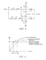
- Fig. 4 is one embodiment of the voltage boosting circuit constructed in accordance with Figs. 2 and 3.
- the voltage boosting circuit of Fig. 4 shows the construction of a charge pump circuit.
- the voltage boosting circuit performs a double pumping operation in response to logic change of a triggered oscillating signal 4)OSC from an oscillator.
- An input node 44 receives the oscillating signal ⁇ OSC generated from the oscillator (not shown).
- a first inverter 46 has an input terminal connected to the input node 44.
- a first pumping capacitor 48 having both terminals of the electrode connected between the first inverter 46 and a first pumping node 50 pumps the first pumping node 50 in response to the voltage level of the output signal of the first inverter 46.
- a first precharge transistor 52 precharges the first pumping node 50 to a voltage level VCC-Vtn.
- a first bipolar transistor 54 of an NPN transistor has the base and collector commonly connected to the first pumping node 50 and the emitter connected to a boosting node 72 for generating the boosting voltage VPP.
- a second inverter 60 has an input terminal connected to the input node 44, and a third inverter 62 has an input terminal connected to the output terminal of the second inverter 60.
- a second pumping capacitor 64 having both terminals of the electrode connected between the third inverter 62 and a second pumping node 66 pumps the second pumping node 66 in response to the voltage level of the output signal of the third inverter 62.
- a second precharge transistor 68 precharges the second pumping node 66 to the voltage level VCC-Vtn.
- a second bipolar transistor 70 of an NPN transistor has the base and collector commonly connected to the second pumping node 66 and the emitter connected to the boosting node 72.
- a third precharge transistor 56 having the channel connected between a supply voltage VCC terminal and the first pumping node 50 and having the gate connected to the second pumping node 66 precharges the first pumping node 50 to the supply voltage VCC level.
- a fourth precharge transistor 58 having the channel connected between the second pumping node 66 and the supply voltage VCC terminal and having the gate connected to the first pumping node 50 precharges the second pumping node 66 to the supply voltage VCC level.
- the structure of Fig. 4 has a feature that the charge pump circuit uses a bipolar transistor as the transmission transistor.
- the operation of the circuit of Fig. 4 will now be discussed.
- the voltage boosting circuit of Fig. 4 is a disabled state, by maintaining the boosting voltage VPP at a desired level or before the chip is enabled, the pumping nodes 50 and 66 are precharged to the voltage level VCC-Vtn by the precharge operation of the first and second precharge transistors 52 and 68.
- Vtn is the threshold voltage of the precharge transistor 52 or 68 of an NMOS transistor.
- the voltage boosting circuit of Fig. 4 is enabled.
- the oscillating signal ⁇ OSC is supplied to the input node 44 as a square wave having a constant period.
- the first inverter 46 generates logic "low”. There is no pumping operation through the first pumping capacitor 48 and the first pumping node 50 maintains its precharge level.
- the second and third inverters 60 and 62 generate logic "low” and "high”, respectively.
- the second pumping capacitor 64 boosts the second pumping node 66 to twice the voltage level VCC-Vtn.
- the boosted voltage level of the second pumping node 66 is transmitted through the second bipolar transistor 70 to the boosting node 72 to raise the boosting voltage VPP.
- the second bipolar transistor 70 is a device formed by the structure of Fig. 3.
- the second bipolar transistor 70 has the device characteristics described in reference to Fig. 3.
- the emitter of the first or second bipolar transistor 54 or 70 corresponds to the n + layer 42 within the P-well 32 of Fig. 3, the base of which is the p + layer 40 within the P-well 32 of Fig. 3, and the collector of which is the n + layer 38 within the N-well 30 of Fig. 3.
- the first inverter 46 Second, if the oscillating signal 4)OSC supplied to the input node 44 is lowered from logic “high” to “low”, the first inverter 46 generates logic "high”.
- the first pumping capacitor 48 pumps the first pumping node 50 from the previous precharge level VCC (this level is obtained through the third precharge transistor 56 in the aforementioned process) to twice the precharge level VCC.
- the boosted voltage level of the pumping node 50 is transmitted to the boosting node 72 via the first bipolar transistor 54 to raise the boosting voltage VPP to a higher level than the previous boosting voltage level.
- the first bipolar transistor 54 is also formed by the structure of Fig. 3 and the device characteristics described in reference to Fig. 3 are maintained during the charge sharing operation of the first pumping node 50 and the boosting node 72 through the first bipolar transistor 54. Therefore, the high voltage charged to the pumping node 50 is transmitted to the boosting node 72 at high speed, and the body effect caused by the raised voltage of the boosting node 72 is prevented.
- the second and third inverters 60 and 62 generate logic "high” and "low” respectively.
- the voltage level 2VCC pumped at the first pumping node 50 fully turns on the channel of the fourth precharge transistor 58 to precharge the second pumping node 66 to the supply voltage VCC level. Consequently, the efficiency of the next pumping operation is raised.
- the aforementioned first process is repeated.
- the precharge level of the first pumping node 50 becomes the supply voltage VCC level and then the pumping operation proceeds.
- a succession of processes is repeated until the boosting voltage VPP is raised to the desired boosting voltage level, and through these processes the boosting voltage VPP is raised to the prescribed voltage level.
- Fig. 5 shows a rising slope of the boosting voltage VPP resulting from the operating characteristics of Fig. 4.
- the inventive voltage boosting circuit has a faster set-up time to raise the boosting voltage VPP to a desired boosting voltage level (about twice the supply voltage VCC) than the conventional circuit. It is apparent that these characteristics can be achieved by the first and second bipolar transistors 54 and 70 of Fig. 4 constructed in accordance with the structure of Fig. 3.
- the voltage boosting circuit embodying the present invention raises the boosting voltage VPP to a desired boosting voltage level by achieving a charge pump circuit having a bipolar transistor. Even if the boosting voltage VPP across the boosting node is raised, the boosting efficiency is raised since there are no current variations flowing into the boosting node. Further, body effect which increases in proportion to the raised boosting voltage in a typical voltage boosting circuit is prevented.
Landscapes
- Power Engineering (AREA)
- Engineering & Computer Science (AREA)
- Microelectronics & Electronic Packaging (AREA)
- General Physics & Mathematics (AREA)
- Condensed Matter Physics & Semiconductors (AREA)
- Computer Hardware Design (AREA)
- Physics & Mathematics (AREA)
- Dram (AREA)
- Dc-Dc Converters (AREA)
- Semiconductor Integrated Circuits (AREA)
- Logic Circuits (AREA)
- Bipolar Integrated Circuits (AREA)
- Amplifiers (AREA)
- Static Random-Access Memory (AREA)
Applications Claiming Priority (2)
| Application Number | Priority Date | Filing Date | Title |
|---|---|---|---|
| KR1019930024483A KR0157334B1 (ko) | 1993-11-17 | 1993-11-17 | 반도체 메모리 장치의 전압 승압회로 |
| KR9324483 | 1993-11-17 |
Publications (3)
| Publication Number | Publication Date |
|---|---|
| EP0653760A2 true EP0653760A2 (de) | 1995-05-17 |
| EP0653760A3 EP0653760A3 (de) | 1995-11-22 |
| EP0653760B1 EP0653760B1 (de) | 2001-04-11 |
Family
ID=19368290
Family Applications (1)
| Application Number | Title | Priority Date | Filing Date |
|---|---|---|---|
| EP94118160A Expired - Lifetime EP0653760B1 (de) | 1993-11-17 | 1994-11-17 | Spannungserhöhungsschaltung |
Country Status (8)
| Country | Link |
|---|---|
| US (2) | US5521871A (de) |
| EP (1) | EP0653760B1 (de) |
| JP (1) | JP3550197B2 (de) |
| KR (1) | KR0157334B1 (de) |
| CN (1) | CN1107955C (de) |
| DE (1) | DE69427066T2 (de) |
| RU (1) | RU2138085C1 (de) |
| TW (1) | TW247969B (de) |
Cited By (1)
| Publication number | Priority date | Publication date | Assignee | Title |
|---|---|---|---|---|
| US8035626B2 (en) | 2002-11-29 | 2011-10-11 | Semiconductor Energy Laboratory Co., Ltd. | Current driving circuit and display device using the current driving circuit |
Families Citing this family (31)
| Publication number | Priority date | Publication date | Assignee | Title |
|---|---|---|---|---|
| JP3102833B2 (ja) | 1994-09-06 | 2000-10-23 | 株式会社 沖マイクロデザイン | 昇圧回路 |
| KR0145615B1 (ko) * | 1995-03-13 | 1998-12-01 | 김광호 | 박막 트랜지스터 액정 표시장치의 구동장치 |
| US5698877A (en) * | 1995-10-31 | 1997-12-16 | Gonzalez; Fernando | Charge-pumping to increase electron collection efficiency |
| GB2308513B (en) * | 1995-12-20 | 2000-11-22 | Hyundai Electronics Ind | Negative voltage drive circuit |
| US5703827A (en) * | 1996-02-29 | 1997-12-30 | Monolithic System Technology, Inc. | Method and structure for generating a boosted word line voltage and a back bias voltage for a memory array |
| EP0822556B1 (de) * | 1996-08-02 | 2003-04-02 | STMicroelectronics S.r.l. | Bidirektionale Ladungspumpe |
| KR100248865B1 (ko) * | 1996-12-14 | 2000-03-15 | 윤종용 | 반도체 장치의 챠지 펌프 회로 |
| US5933047A (en) * | 1997-04-30 | 1999-08-03 | Mosaid Technologies Incorporated | High voltage generating circuit for volatile semiconductor memories |
| US6011423A (en) * | 1997-05-23 | 2000-01-04 | International Business Machines Corporation | Virtual voltage power supply |
| US5784326A (en) * | 1997-06-04 | 1998-07-21 | Holtek Microelectronics Inc. | Voltage raising device |
| JPH1145574A (ja) * | 1997-07-25 | 1999-02-16 | Nec Corp | 半導体記憶装置 |
| US6188265B1 (en) * | 1997-12-12 | 2001-02-13 | Scenix Semiconduction, Inc. | High-voltage NMOS switch |
| KR100279296B1 (ko) * | 1998-06-09 | 2001-01-15 | 윤종용 | 승압 전압 발생 회로 |
| US6977420B2 (en) * | 1998-09-30 | 2005-12-20 | National Semiconductor Corporation | ESD protection circuit utilizing floating lateral clamp diodes |
| US6078211A (en) * | 1998-10-14 | 2000-06-20 | National Semiconductor Corporation | Substrate biasing circuit that utilizes a gated diode to set the bias on the substrate |
| US6380571B1 (en) | 1998-10-14 | 2002-04-30 | National Semiconductor Corporation | CMOS compatible pixel cell that utilizes a gated diode to reset the cell |
| US6072725A (en) * | 1999-01-26 | 2000-06-06 | Advanced Micro Devices, Inc. | Method of erasing floating gate capacitor used in voltage regulator |
| US6064594A (en) * | 1999-02-26 | 2000-05-16 | Stmicroelectronics S.R.L. | Voltage boosting circuit for generating boosted voltage phases |
| DE19924568B4 (de) * | 1999-05-28 | 2014-05-22 | Qimonda Ag | Ladungspumpe |
| US6255896B1 (en) * | 1999-09-27 | 2001-07-03 | Intel Corporation | Method and apparatus for rapid initialization of charge pump circuits |
| US6346846B1 (en) | 1999-12-17 | 2002-02-12 | International Business Machines Corporation | Methods and apparatus for blowing and sensing antifuses |
| US6356137B1 (en) * | 2000-06-26 | 2002-03-12 | Fairchild Semiconductor Corporation | Voltage boost circuit with low power supply voltage |
| US6504422B1 (en) * | 2000-11-21 | 2003-01-07 | Semtech Corporation | Charge pump with current limiting circuit |
| KR100796782B1 (ko) * | 2005-12-13 | 2008-01-22 | 삼성전자주식회사 | 반도체 메모리 장치의 승압전압 발생회로 및 승압전압발생방법 |
| JP4883780B2 (ja) * | 2006-11-14 | 2012-02-22 | ルネサスエレクトロニクス株式会社 | チャージポンプ回路 |
| KR100850272B1 (ko) * | 2007-01-25 | 2008-08-04 | 삼성전자주식회사 | 반도체 메모리 장치의 전압 발생회로 및 사용 전압공급방법 |
| US7859301B2 (en) * | 2007-04-30 | 2010-12-28 | Altera Corporation | Power regulator circuitry for programmable logic device memory elements |
| JP4985208B2 (ja) * | 2007-08-10 | 2012-07-25 | 株式会社デンソー | 倍電圧整流回路 |
| JP5467454B2 (ja) * | 2009-09-01 | 2014-04-09 | Nltテクノロジー株式会社 | ブートストラップ回路及びレベルシフト回路並びにワード線駆動回路 |
| US9281682B2 (en) * | 2013-03-12 | 2016-03-08 | Micron Technology, Inc. | Apparatuses and method for over-voltage event protection |
| US11791332B2 (en) | 2021-02-26 | 2023-10-17 | Taiwan Semiconductor Manufacturing Co., Ltd. | Stacked semiconductor device and method |
Citations (4)
| Publication number | Priority date | Publication date | Assignee | Title |
|---|---|---|---|---|
| EP0407111A2 (de) * | 1989-07-01 | 1991-01-09 | Plessey Semiconductors Limited | Verfahren zur Herstellung einer Diffusionskollektor-Isolationshalbleitervorrichtung |
| EP0439899A2 (de) * | 1990-01-25 | 1991-08-07 | Precision Monolithics Inc. | Für CMOS-Prozesse geeignete komplementäre Bipolartransistoren |
| US5043858A (en) * | 1988-07-14 | 1991-08-27 | Nec Corporation | High-voltage generating circuit having improved voltage boosting efficiency |
| DE4237589A1 (en) * | 1991-11-07 | 1993-05-19 | Samsung Electronics Co Ltd | Semiconductor memory device with voltage pumping circuit - comprises oscillator for generating pulses, and voltage pumping circuit for generating at initial power-up state, first output voltage equal to supply voltage |
Family Cites Families (9)
| Publication number | Priority date | Publication date | Assignee | Title |
|---|---|---|---|---|
| JPS6085493A (ja) * | 1983-10-17 | 1985-05-14 | Hitachi Ltd | ブ−トストラツプ回路 |
| JP2548908B2 (ja) * | 1985-04-13 | 1996-10-30 | 富士通株式会社 | 昇圧回路 |
| JP2580226B2 (ja) * | 1988-02-16 | 1997-02-12 | 株式会社日立製作所 | 半導体集積回路装置 |
| US4996453A (en) * | 1989-07-28 | 1991-02-26 | Dallas Semiconductor | Power down circuit for low-power circuit with dual supply voltages |
| IT1258242B (it) * | 1991-11-07 | 1996-02-22 | Samsung Electronics Co Ltd | Dispositivo di memoria a semiconduttore includente circuiteria di pompaggio della tensione di alimentazione |
| JP2771729B2 (ja) * | 1992-04-16 | 1998-07-02 | 三菱電機株式会社 | チャージポンプ回路 |
| KR950006067Y1 (ko) * | 1992-10-08 | 1995-07-27 | 문정환 | 반도체 메모리 장치 |
| KR960000837B1 (ko) * | 1992-12-02 | 1996-01-13 | 삼성전자주식회사 | 반도체 메모리장치 |
| JP3307453B2 (ja) * | 1993-03-18 | 2002-07-24 | ソニー株式会社 | 昇圧回路 |
-
1993
- 1993-11-17 KR KR1019930024483A patent/KR0157334B1/ko not_active IP Right Cessation
-
1994
- 1994-11-16 JP JP28175594A patent/JP3550197B2/ja not_active Expired - Fee Related
- 1994-11-16 RU RU94045859A patent/RU2138085C1/ru not_active IP Right Cessation
- 1994-11-17 EP EP94118160A patent/EP0653760B1/de not_active Expired - Lifetime
- 1994-11-17 US US08/342,050 patent/US5521871A/en not_active Expired - Lifetime
- 1994-11-17 DE DE69427066T patent/DE69427066T2/de not_active Expired - Fee Related
- 1994-11-17 CN CN94118947A patent/CN1107955C/zh not_active Expired - Fee Related
- 1994-11-22 TW TW083110841A patent/TW247969B/zh active
-
1995
- 1995-09-15 US US08/526,499 patent/US5610549A/en not_active Expired - Lifetime
Patent Citations (4)
| Publication number | Priority date | Publication date | Assignee | Title |
|---|---|---|---|---|
| US5043858A (en) * | 1988-07-14 | 1991-08-27 | Nec Corporation | High-voltage generating circuit having improved voltage boosting efficiency |
| EP0407111A2 (de) * | 1989-07-01 | 1991-01-09 | Plessey Semiconductors Limited | Verfahren zur Herstellung einer Diffusionskollektor-Isolationshalbleitervorrichtung |
| EP0439899A2 (de) * | 1990-01-25 | 1991-08-07 | Precision Monolithics Inc. | Für CMOS-Prozesse geeignete komplementäre Bipolartransistoren |
| DE4237589A1 (en) * | 1991-11-07 | 1993-05-19 | Samsung Electronics Co Ltd | Semiconductor memory device with voltage pumping circuit - comprises oscillator for generating pulses, and voltage pumping circuit for generating at initial power-up state, first output voltage equal to supply voltage |
Non-Patent Citations (3)
| Title |
|---|
| MILLMAN ET AL. 'INTEGRATED ELECTRONICS:ANALOG AND DIGITAL CIRCUITS AND SYSTEMS' 1972 , MCGRAW HILL KOGAKUSHA LTD , TOKYO * page 214, line 20 - page 215, line 10; figure 7.16 * * |
| U. TIETZE-CH. SCHENK, Halbleiterschaltungstechnik, Springer Verlag Berlin, 1974, pages 35-36 * |
| WIRELESS WORLD, vol.89, no.1573, October 1983, HAYWARDS HEATH GB pages 59 - 59 'CHEAP VOLTAGE DOUBLER' * |
Cited By (3)
| Publication number | Priority date | Publication date | Assignee | Title |
|---|---|---|---|---|
| US8035626B2 (en) | 2002-11-29 | 2011-10-11 | Semiconductor Energy Laboratory Co., Ltd. | Current driving circuit and display device using the current driving circuit |
| US8395607B2 (en) | 2002-11-29 | 2013-03-12 | Semiconductor Energy Laboratory Co., Ltd. | Current driving circuit and display device using the current driving circuit |
| US8605064B2 (en) | 2002-11-29 | 2013-12-10 | Semiconductor Energy Laboratory Co., Ltd. | Current driving circuit and display device using the current driving circuit |
Also Published As
| Publication number | Publication date |
|---|---|
| CN1107955C (zh) | 2003-05-07 |
| RU2138085C1 (ru) | 1999-09-20 |
| EP0653760B1 (de) | 2001-04-11 |
| DE69427066T2 (de) | 2001-10-11 |
| RU94045859A (ru) | 1996-09-27 |
| EP0653760A3 (de) | 1995-11-22 |
| US5521871A (en) | 1996-05-28 |
| JP3550197B2 (ja) | 2004-08-04 |
| CN1122943A (zh) | 1996-05-22 |
| US5610549A (en) | 1997-03-11 |
| TW247969B (de) | 1995-05-21 |
| KR950015769A (ko) | 1995-06-17 |
| KR0157334B1 (ko) | 1998-10-15 |
| JPH07183471A (ja) | 1995-07-21 |
| DE69427066D1 (de) | 2001-05-17 |
Similar Documents
| Publication | Publication Date | Title |
|---|---|---|
| EP0653760B1 (de) | Spannungserhöhungsschaltung | |
| US5315166A (en) | Substrate voltage generator and method therefor in a semiconductor device having selectively activated internal stepped-down power supply voltages | |
| JP2516296B2 (ja) | ワ―ドライン駆動回路 | |
| EP0463545B1 (de) | Substratvorspannungsgenerator für Halbleiteranordnungen | |
| US5255224A (en) | Boosted drive system for master/local word line memory architecture | |
| WO1997032310A1 (en) | A boosted word line driver circuit | |
| US5521546A (en) | Voltage boosting circuit constructed on an integrated circuit substrate, as for a semiconductor memory device | |
| US5757714A (en) | Semiconductor memory device with on-chip boosted power supply voltage generator | |
| KR940010837B1 (ko) | Dram의 워드선 구동회로 | |
| US6288601B1 (en) | Boosted potential generating circuit | |
| US6316985B1 (en) | Substrate voltage generating circuit provided with a transistor having a thin gate oxide film and a semiconductor integrated circuit device provided with the same | |
| US6225854B1 (en) | Voltage boosting circuit having cross-coupled precharge circuits | |
| US5179535A (en) | Substrate bias voltage generating circuit including an internal frequency divider and driven by an externally applied clock signal | |
| US7382177B2 (en) | Voltage charge pump and method of operating the same | |
| JP2632112B2 (ja) | 電圧発生回路 | |
| IE50579B1 (en) | Bootstrap circuit | |
| US6175263B1 (en) | Back bias generator having transfer transistor with well bias | |
| US5134317A (en) | Booster circuit for a semiconductor memory device | |
| US6198341B1 (en) | Substrate bias voltage generating circuit for use in a semiconductor device | |
| US5579276A (en) | Internal voltage boosting circuit in a semiconductor memory device | |
| JP2748733B2 (ja) | 半導体メモリ | |
| US5266843A (en) | Substrate slew circuit | |
| KR100238867B1 (ko) | 반도체 메모리 장치의 승압회로 | |
| KR0170286B1 (ko) | 반도체 메모리장치의 전압 승압회로 | |
| KR100432985B1 (ko) | 상승된출력전압을발생시키기위한회로 |
Legal Events
| Date | Code | Title | Description |
|---|---|---|---|
| PUAI | Public reference made under article 153(3) epc to a published international application that has entered the european phase |
Free format text: ORIGINAL CODE: 0009012 |
|
| AK | Designated contracting states |
Kind code of ref document: A2 Designated state(s): DE FR GB IT NL |
|
| PUAL | Search report despatched |
Free format text: ORIGINAL CODE: 0009013 |
|
| AK | Designated contracting states |
Kind code of ref document: A3 Designated state(s): DE FR GB IT NL |
|
| 17P | Request for examination filed |
Effective date: 19960417 |
|
| 17Q | First examination report despatched |
Effective date: 19980626 |
|
| GRAG | Despatch of communication of intention to grant |
Free format text: ORIGINAL CODE: EPIDOS AGRA |
|
| GRAG | Despatch of communication of intention to grant |
Free format text: ORIGINAL CODE: EPIDOS AGRA |
|
| GRAH | Despatch of communication of intention to grant a patent |
Free format text: ORIGINAL CODE: EPIDOS IGRA |
|
| GRAH | Despatch of communication of intention to grant a patent |
Free format text: ORIGINAL CODE: EPIDOS IGRA |
|
| GRAA | (expected) grant |
Free format text: ORIGINAL CODE: 0009210 |
|
| AK | Designated contracting states |
Kind code of ref document: B1 Designated state(s): DE FR GB IT NL |
|
| REF | Corresponds to: |
Ref document number: 69427066 Country of ref document: DE Date of ref document: 20010517 |
|
| ITF | It: translation for a ep patent filed | ||
| ET | Fr: translation filed | ||
| REG | Reference to a national code |
Ref country code: GB Ref legal event code: IF02 |
|
| PLBE | No opposition filed within time limit |
Free format text: ORIGINAL CODE: 0009261 |
|
| STAA | Information on the status of an ep patent application or granted ep patent |
Free format text: STATUS: NO OPPOSITION FILED WITHIN TIME LIMIT |
|
| 26N | No opposition filed | ||
| PGFP | Annual fee paid to national office [announced via postgrant information from national office to epo] |
Ref country code: NL Payment date: 20071104 Year of fee payment: 14 Ref country code: DE Payment date: 20071115 Year of fee payment: 14 |
|
| PGFP | Annual fee paid to national office [announced via postgrant information from national office to epo] |
Ref country code: IT Payment date: 20071127 Year of fee payment: 14 |
|
| PGFP | Annual fee paid to national office [announced via postgrant information from national office to epo] |
Ref country code: GB Payment date: 20071114 Year of fee payment: 14 Ref country code: FR Payment date: 20071108 Year of fee payment: 14 |
|
| GBPC | Gb: european patent ceased through non-payment of renewal fee |
Effective date: 20081117 |
|
| PG25 | Lapsed in a contracting state [announced via postgrant information from national office to epo] |
Ref country code: NL Free format text: LAPSE BECAUSE OF NON-PAYMENT OF DUE FEES Effective date: 20090601 |
|
| NLV4 | Nl: lapsed or anulled due to non-payment of the annual fee |
Effective date: 20090601 |
|
| PG25 | Lapsed in a contracting state [announced via postgrant information from national office to epo] |
Ref country code: IT Free format text: LAPSE BECAUSE OF NON-PAYMENT OF DUE FEES Effective date: 20081117 |
|
| REG | Reference to a national code |
Ref country code: FR Ref legal event code: ST Effective date: 20090731 |
|
| PG25 | Lapsed in a contracting state [announced via postgrant information from national office to epo] |
Ref country code: DE Free format text: LAPSE BECAUSE OF NON-PAYMENT OF DUE FEES Effective date: 20090603 |
|
| PG25 | Lapsed in a contracting state [announced via postgrant information from national office to epo] |
Ref country code: GB Free format text: LAPSE BECAUSE OF NON-PAYMENT OF DUE FEES Effective date: 20081117 |
|
| PG25 | Lapsed in a contracting state [announced via postgrant information from national office to epo] |
Ref country code: FR Free format text: LAPSE BECAUSE OF NON-PAYMENT OF DUE FEES Effective date: 20081130 |