EP0642164A2 - Dünnes vertikales stapelbares Gehäuse und "lead-on-chip" Speicherwürfel aus gegossenem Kunststoff - Google Patents
Dünnes vertikales stapelbares Gehäuse und "lead-on-chip" Speicherwürfel aus gegossenem Kunststoff Download PDFInfo
- Publication number
- EP0642164A2 EP0642164A2 EP94111578A EP94111578A EP0642164A2 EP 0642164 A2 EP0642164 A2 EP 0642164A2 EP 94111578 A EP94111578 A EP 94111578A EP 94111578 A EP94111578 A EP 94111578A EP 0642164 A2 EP0642164 A2 EP 0642164A2
- Authority
- EP
- European Patent Office
- Prior art keywords
- chip
- package
- lead frame
- conductors
- major surface
- Prior art date
- Legal status (The legal status is an assumption and is not a legal conclusion. Google has not performed a legal analysis and makes no representation as to the accuracy of the status listed.)
- Withdrawn
Links
Images




Classifications
-
- H—ELECTRICITY
- H10—SEMICONDUCTOR DEVICES; ELECTRIC SOLID-STATE DEVICES NOT OTHERWISE PROVIDED FOR
- H10W—GENERIC PACKAGES, INTERCONNECTIONS, CONNECTORS OR OTHER CONSTRUCTIONAL DETAILS OF DEVICES COVERED BY CLASS H10
- H10W70/00—Package substrates; Interposers; Redistribution layers [RDL]
- H10W70/40—Leadframes
- H10W70/411—Chip-supporting parts, e.g. die pads
- H10W70/415—Leadframe inner leads serving as die pads
-
- H—ELECTRICITY
- H10—SEMICONDUCTOR DEVICES; ELECTRIC SOLID-STATE DEVICES NOT OTHERWISE PROVIDED FOR
- H10W—GENERIC PACKAGES, INTERCONNECTIONS, CONNECTORS OR OTHER CONSTRUCTIONAL DETAILS OF DEVICES COVERED BY CLASS H10
- H10W40/00—Arrangements for thermal protection or thermal control
- H10W40/20—Arrangements for cooling
- H10W40/22—Arrangements for cooling characterised by their shape, e.g. having conical or cylindrical projections
- H10W40/226—Arrangements for cooling characterised by their shape, e.g. having conical or cylindrical projections characterised by projecting parts, e.g. fins to increase surface area
-
- H—ELECTRICITY
- H10—SEMICONDUCTOR DEVICES; ELECTRIC SOLID-STATE DEVICES NOT OTHERWISE PROVIDED FOR
- H10W—GENERIC PACKAGES, INTERCONNECTIONS, CONNECTORS OR OTHER CONSTRUCTIONAL DETAILS OF DEVICES COVERED BY CLASS H10
- H10W42/00—Arrangements for protection of devices
- H10W42/20—Arrangements for protection of devices protecting against electromagnetic or particle radiation, e.g. light, X-rays, gamma-rays or electrons
-
- H—ELECTRICITY
- H10—SEMICONDUCTOR DEVICES; ELECTRIC SOLID-STATE DEVICES NOT OTHERWISE PROVIDED FOR
- H10W—GENERIC PACKAGES, INTERCONNECTIONS, CONNECTORS OR OTHER CONSTRUCTIONAL DETAILS OF DEVICES COVERED BY CLASS H10
- H10W90/00—Package configurations
-
- H—ELECTRICITY
- H10—SEMICONDUCTOR DEVICES; ELECTRIC SOLID-STATE DEVICES NOT OTHERWISE PROVIDED FOR
- H10W—GENERIC PACKAGES, INTERCONNECTIONS, CONNECTORS OR OTHER CONSTRUCTIONAL DETAILS OF DEVICES COVERED BY CLASS H10
- H10W70/00—Package substrates; Interposers; Redistribution layers [RDL]
- H10W70/40—Leadframes
-
- H—ELECTRICITY
- H10—SEMICONDUCTOR DEVICES; ELECTRIC SOLID-STATE DEVICES NOT OTHERWISE PROVIDED FOR
- H10W—GENERIC PACKAGES, INTERCONNECTIONS, CONNECTORS OR OTHER CONSTRUCTIONAL DETAILS OF DEVICES COVERED BY CLASS H10
- H10W72/00—Interconnections or connectors in packages
- H10W72/50—Bond wires
- H10W72/541—Dispositions of bond wires
- H10W72/5449—Dispositions of bond wires not being orthogonal to a side surface of the chip, e.g. fan-out arrangements
-
- H—ELECTRICITY
- H10—SEMICONDUCTOR DEVICES; ELECTRIC SOLID-STATE DEVICES NOT OTHERWISE PROVIDED FOR
- H10W—GENERIC PACKAGES, INTERCONNECTIONS, CONNECTORS OR OTHER CONSTRUCTIONAL DETAILS OF DEVICES COVERED BY CLASS H10
- H10W72/00—Interconnections or connectors in packages
- H10W72/50—Bond wires
- H10W72/551—Materials of bond wires
- H10W72/552—Materials of bond wires comprising metals or metalloids, e.g. silver
- H10W72/5522—Materials of bond wires comprising metals or metalloids, e.g. silver comprising gold [Au]
-
- H—ELECTRICITY
- H10—SEMICONDUCTOR DEVICES; ELECTRIC SOLID-STATE DEVICES NOT OTHERWISE PROVIDED FOR
- H10W—GENERIC PACKAGES, INTERCONNECTIONS, CONNECTORS OR OTHER CONSTRUCTIONAL DETAILS OF DEVICES COVERED BY CLASS H10
- H10W74/00—Encapsulations, e.g. protective coatings
-
- H—ELECTRICITY
- H10—SEMICONDUCTOR DEVICES; ELECTRIC SOLID-STATE DEVICES NOT OTHERWISE PROVIDED FOR
- H10W—GENERIC PACKAGES, INTERCONNECTIONS, CONNECTORS OR OTHER CONSTRUCTIONAL DETAILS OF DEVICES COVERED BY CLASS H10
- H10W90/00—Package configurations
- H10W90/20—Configurations of stacked chips
- H10W90/288—Configurations of stacked chips characterised by arrangements for thermal management of the stacked chips
-
- H—ELECTRICITY
- H10—SEMICONDUCTOR DEVICES; ELECTRIC SOLID-STATE DEVICES NOT OTHERWISE PROVIDED FOR
- H10W—GENERIC PACKAGES, INTERCONNECTIONS, CONNECTORS OR OTHER CONSTRUCTIONAL DETAILS OF DEVICES COVERED BY CLASS H10
- H10W90/00—Package configurations
- H10W90/701—Package configurations characterised by the relative positions of pads or connectors relative to package parts
- H10W90/721—Package configurations characterised by the relative positions of pads or connectors relative to package parts of bump connectors
- H10W90/722—Package configurations characterised by the relative positions of pads or connectors relative to package parts of bump connectors between stacked chips
-
- H—ELECTRICITY
- H10—SEMICONDUCTOR DEVICES; ELECTRIC SOLID-STATE DEVICES NOT OTHERWISE PROVIDED FOR
- H10W—GENERIC PACKAGES, INTERCONNECTIONS, CONNECTORS OR OTHER CONSTRUCTIONAL DETAILS OF DEVICES COVERED BY CLASS H10
- H10W90/00—Package configurations
- H10W90/701—Package configurations characterised by the relative positions of pads or connectors relative to package parts
- H10W90/751—Package configurations characterised by the relative positions of pads or connectors relative to package parts of bond wires
- H10W90/756—Package configurations characterised by the relative positions of pads or connectors relative to package parts of bond wires between a chip and a stacked lead frame, conducting package substrate or heat sink
-
- Y—GENERAL TAGGING OF NEW TECHNOLOGICAL DEVELOPMENTS; GENERAL TAGGING OF CROSS-SECTIONAL TECHNOLOGIES SPANNING OVER SEVERAL SECTIONS OF THE IPC; TECHNICAL SUBJECTS COVERED BY FORMER USPC CROSS-REFERENCE ART COLLECTIONS [XRACs] AND DIGESTS
- Y10—TECHNICAL SUBJECTS COVERED BY FORMER USPC
- Y10T—TECHNICAL SUBJECTS COVERED BY FORMER US CLASSIFICATION
- Y10T29/00—Metal working
- Y10T29/49—Method of mechanical manufacture
- Y10T29/49002—Electrical device making
- Y10T29/49117—Conductor or circuit manufacturing
- Y10T29/49121—Beam lead frame or beam lead device
-
- Y—GENERAL TAGGING OF NEW TECHNOLOGICAL DEVELOPMENTS; GENERAL TAGGING OF CROSS-SECTIONAL TECHNOLOGIES SPANNING OVER SEVERAL SECTIONS OF THE IPC; TECHNICAL SUBJECTS COVERED BY FORMER USPC CROSS-REFERENCE ART COLLECTIONS [XRACs] AND DIGESTS
- Y10—TECHNICAL SUBJECTS COVERED BY FORMER USPC
- Y10T—TECHNICAL SUBJECTS COVERED BY FORMER US CLASSIFICATION
- Y10T29/00—Metal working
- Y10T29/49—Method of mechanical manufacture
- Y10T29/49002—Electrical device making
- Y10T29/49117—Conductor or circuit manufacturing
- Y10T29/49169—Assembling electrical component directly to terminal or elongated conductor
- Y10T29/49171—Assembling electrical component directly to terminal or elongated conductor with encapsulating
- Y10T29/49172—Assembling electrical component directly to terminal or elongated conductor with encapsulating by molding of insulating material
Definitions
- This invention relates to lead bonded semiconductor chips. More particularly it relates to the so-called Lead-On-Chip (LOC) package configuration arranged in a stack and a method of creating the stack. Each package is created to be of minimum size, and provided with a thermal heat sink arranged with respect to the remainder of the package to balance the stresses in the package.
- LOC Lead-On-Chip
- LOC packages are now well known to the semiconductor industry and are fully described in USP 4,862,245 assigned to the same assignee as the present invention. Heat sinks have also been attached to the backside, i.e. the nonactive face, of semiconductor chips as shown in USP 3,922,712. USP 4,868,712 discloses a stack of semiconductor devices with heat sinks attached thereto.
- Circuits formed in semiconductor chips have, over the years, become small, fast and dense yet the demands of the users require still smaller, faster and denser configurations which impose unique package size and thermal conditions.
- This invention provides a still smaller size, than any now known to the prior art, with improved electrical and thermal characteristics.
- An object of the present invention is to provide an ultra-thin package for a semiconductor chip, using LOC technology, which meets the size and thermal conditions presently required by the industry. This desirable result is accomplished by the encapsulation of a chip, with a plastic encapsulating material, on at least five of its six sides while attaching the heat sink directly to the sixth side of the chip.
- the heat sink be designed to balance the stresses on the chip introduced by the application of the leads on the active chip face and the encapsulation.
- the heat sink is comprised of a metal capable of thermally conducting and dissipating waste heat away from the chip and is of a mass, thickness, and area to counterbalance stresses such, as bending stresses, introduced into the chip by the application of the lead frame and encapsulant to the chip.
- the heat sink can also be employed as a ground plane to provide an electromagnetic shield when the chips are arranged in a stack.
- Fig. 1 shows a typical lead frame as might be used in the present invention.
- Fig. 2 shows a semiconductor chip on which the lead frame of Fig. 1 is positioned and bonded using wire bonds.
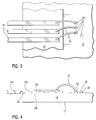
- Fig. 3 shows a top view of a selected portion of the lead frame of Fig.1 illustrating the wires bonding the lead frame to the chip.
- Fig 4 shows a side view of the portion of the lead frame illustrated in Fig. 3.
- Fig. 5 shows a top view of a selected portion of the lead frame illustrating a different embodiment of bonding the lead frame to the chip.
- Fig 6 shows a side view of the portion of the lead frame illustrated in Fig. 5.
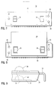
- Fig. 7 shows the top view of an encapsulated chip in accordance with the present invention.
- Fig. 8 shows the bottom view of an encapsulated chip in accordance with the present invention.
- Fig. 9 shows side view of the encapsulated chip of Figs. 7 and 8.
- Fig. 10 illustrates a molded memory cube in accordance with the present invention.
- Fig. 1 is a top view of a lead frame as would be used in the present invention.
- the lead frame 10 is produced from metal sheet stock and formed with a plurality of indexing holes 12 and provided with a plurality of extended conductors 14.
- Such lead frames are preferably made from a copper alloy and are well known and have a definite meaning in the semiconductor art.
- the material, thickness and strength of such lead frames have been so long known to the art that the use of the term "lead frame” as used in the art is all that is needed to purchase such items.
- the term “lead frame” means a metal structure, preferably a plated copper alloy, formed of sheet stock of a sufficient size and strength to meet specific mechanical strength requirements.
- the lead frame is typically formed of sheet stock between 0.125 and 0.195 millimeters (mm) thick and the individual conductors are between 0.2 and 0.5 mm wide.
- Figs. 2, 3, and 4 show a semiconductor chip 18 having first and second major surfaces 16 and 17, i.e. the front and back sides, substantially parallel to each other and four edges or minor sides 19a, 19b, 19c, and 19d, perpendicular to and joining said major surfaces.
- One major surface, i.e. major surface 16 is the active face of the chip in which integrated circuits are formed and input/output pads 24 are disposed and the other major surface is the back or substrate side of the chip.
- the lead frame of Fig. 1 is positioned on major surface 16 and bonded to the pads 24 using wire bonds.
- the chip 18 is typically 13.8 mm long and 6.8 mm wide and 0.76 mm thick.
- a layer of insulating material 20 is positioned between the lead frame conductors 14 and the underlying portions of the active face 16.
- the layer 20 is a polymer film which can stand a temperature in excess of 175 degrees Celsius and does not contain ionizable species such as halide and active metals including sodium (Na), potassium (K) and phosphorus (P).
- the layer 20 can be formed, for example, of a 0.05 mm thick polyamide film such as is sold by the DuPont de Nemours under the tradename "Kapton". Such polyamide films can be obtained in varying thickness and for the present invention would be between 0.025 mm and 0.05 mm in thickness. These films are usually, for this invention, thermally enhanced by aluminum and silicon nitride additions thereto.
- the layer 20 has adhesive coatings 20a and 20b, which are applied as thin coatings, in the order of 0.02 mm thick, to the major surfaces of layer 20 and are used to help secure the layer 20 to the lead frame 14 and the chip 10. This layer 20 helps assure that short circuits between the lead frame and the chip do not occur.
- the adhesive layers applied to the different sides of layer 20 can be of different materials, for example, the adhesive coating 20b securing the layer 20 to the semiconductor chip 18 can be selected from the group of epoxies, acrylics silicones and polyimides with epoxies being preferred.
- the other adhesive coating 20a which holds the lead frame conductors to the layer 20 can be selected from the same group of materials with the epoxies, acrylics and polyimides containing phenolics being preferred.
- One material suitable for use as the adhesive layers 20a and 20b is sold by the Rogers Corporation of Chandler, Ariz., under the tradename "Rogers 8970".
- one or more of the above listed adhesives themselves can, if laid down in sufficient thickness to provide the desired insulation qualities can be used in place of the Kapton film.
- Figs. 2 and 3 shows the inner end of the lead frame conductors bonded to the active face of the chip via the insulating layer 20.
- the selvage including the indexing holes 12
- This bonding of the lead frame conductors to the active face 16 of the chip 18 requires heating the assembly to a temperature of about 160 degrees Celsius to fully cure the adhesive used as or in conjunction with the insulating layer 20. It has been found that during cool down of the assembly following this curing step that bending is induced in the silicon chip due to the difference in the thermal expansion rates between the chip, the layer 20 and the lead frame conductors.
- the inner portions or proximal ends 14b of the lead frame conductors 14, i.e. in the region where they overlie the active face of the chip, are typically 0.254 mm wide, and have been thinned to one half thickness of the portion i.e. the distal ends 14a of the conductors extending beyond the edge of the chip.
- the proximal ends 14b of the conductors 14 are reduced in thickness to be typically 0.076 mm and are designed to overly the active face of the chip. It should also be noted that in the example given the distal ends 14a are typically 0.41 mm wide and the proximal ends 14b are reduced in width to typically 0.255 mm in width.
- the stresses applied to the chip 18 and thus the bending of the chip 18, following the epoxy cure step and the application of the proximal ends of the conductors to the active face 16 of the chip 18, is greatly reduced thus substantially reducing if not eliminating the probability of altering the electrical characteristics of the integrated circuit built in the chip.
- This reduced thickness in the conductors also greatly minimizes the likelihood of delamination of the conductors from the underlying adhesive layer.
- a significantly thinner profile package can be realized.
- the inner portions of the conductors are reduced in thickness where they overlie the active face of the chip that portion of the lead frame conductors 14, i.e. the distal ends 14b, which extends beyond the edge of the chip is maintained at full thickness to provide robust leads that are required by the bending and joining procedures to secure the devices to the next level of assembly.
- Figs. 5 and 6 show an alternative to the wire bonding technique.
- the proximal ends 14b of the lead frame conductors 14, instead of terminating on the insulating layer, are extended into tips 14c cantilevered over the pads 24 to which they are to be bonded.
- the tips 14c of the conductors 14 are forced against the pads 24 with a single point thermosonic bonding tool 26 to bond the each of the tips 14c directly to an underlying respective pad 24.
- this method of direct conductor to pad interconnection will further enhance electrical performance by reducing the inductance of the interconnections by the elimination of the gold wire as well as the discontinuity associated with signal reflections between the larger pad 24 and the smaller cross section wire 22.
- the assembly is encapsulated in a suitable plastic material using well known transfer molding techniques.
- the encapsulant 30 is molded around five of the six sides of the chip 18 so as to encase the chip.
- the sixth side remains substantially uncovered with encapsulant so that there is a large recess 32 formed in the encapsulant in which the backside of the chip 18 remains exposed, i.e. unencapsulated.
- an additional thin metallic member typically 0.13 mm thick, in the form of a flat plate 34 can be secured to the chip.
- This plate 34 serves several functions. It not only, by being in good thermal contact with the backside of the chip, serves as a heat sink but also by having a good conductive bond to the ground connection on the chip can serve as a ground plane.
- the first of the above cases is to be used when the bulk silicon, i.e. the substrate, is electrical ground for the circuit formed in the active face.
- This plate 34 when acting as a ground plane improves the current rise time performance by decreasing the ground path inductance and provides better immunity to electrical noise created by mismatch.
- the plate will compensate for any bending moment induced in the chip by the application of the lead frame conductors and the encapsulation step. In this way no net bending defection results in the finished package. Also by extending the plate 34 beyond the edge of the encapsulant it will further enhance the dissipation of heat from the package.
- thermosetting conductive adhesive such as is sold under the tradename AMICON C-991 by the Emerson and Cummings Co. or a modified epoxy amine sold under the tradename ABLEBOND 165-1L by the Ablestick Co. and placed in a suitably formed mold and the chip with the lead frame already attached is placed on the adhesively coated plate and if the adhesive is not conductive any necessary ground connection made to the plate.
- the mold is then closed and the encapsulant injected into the mold at a suitable temperature and pressure.
- the epoxy adhesive used to join the chip to the plate can be cured simultaneously with the curing of the encapsulant material.
- the final phase of package bending can be eliminated.
- the mold by proper design can be made to include a recessed area into which the plate can later be affixed.
- the plate attachment adhesive may then be simultaneously cured with the post mold cure process.
- the mold can be formed to leave suitable openings 36 in both the front and the back of the encapsulant into which decoupling capacitors can be secured.
- These openings 36 are typically 1.8 mm wide and 3.30 mm long and can also be placed such that formed tabs on any capacitor inserted therein may intersect with suitable distal ends of the conductors on the lead frame that extend from the chip.
- Fig. 9 shows an arrangement of the invention particularly adapted for stacking a number of packages in a cube.
- molded protrusions 38 in the form of hemispherical bumps typically having a radius of 0.50 mm are molded in the lead frame side of the package and corresponding matched but slightly larger sockets 40, with a typical radius of 0.60 mm, are formed in the opposite side.
- These bumps and sockets serve to align the packages with one another so they can be stacked together to form a cube.
- Fig. 10 shows a plurality of the packages of Fig. 7 arranged in a stacked configuration.
- This stack is realized by coating the back side of the package with a thermoplastic polyimide adhesive such as is sold by the 3M company under the tradename "Scotch Brand 386". By placing this adhesive on the front surface the back surface of a another package can joined to it.
- the protrusions 38 in the form of hemispherical bumps, molded on the lead frame side of the package mate with the corresponding matched sockets 40 formed in the opposite side.
- These bumps 38 and sockets 40 align each package with any adjacent package so they can be readily and positively stacked one onto the other.
- the stack requires a heating step to cause the adhesive to bond each package securely to the adjacent packages.
- a temperature of about 230 degrees Celsius is used. This temperature is below the melting or softening temperature of any of the materials used in creating the packages, except of course for this adhesive layer. This heating step causes the packages to bond together. In this way any number of packages may be bonded together in a single stack.
- the stack can be tested and used. If, during test or subsequent use, one or more of the packages fail or found to be defective the stack can readily be disassembled. This disassembly can be done by again heating the stack to 210 degrees Celsius at which temperature the stack readily delaminates from the metallic plate. By following this procedure the stack can be easily separated into individual packages, the defective package removed from the stack, replaced with an operating package and the stack reassembled as discussed above.
Landscapes
- Lead Frames For Integrated Circuits (AREA)
- Wire Bonding (AREA)
Applications Claiming Priority (2)
| Application Number | Priority Date | Filing Date | Title |
|---|---|---|---|
| US08/116,320 US5457071A (en) | 1993-09-03 | 1993-09-03 | Stackable vertical thin package/plastic molded lead-on-chip memory cube |
| US116320 | 1993-09-03 |
Publications (2)
| Publication Number | Publication Date |
|---|---|
| EP0642164A2 true EP0642164A2 (de) | 1995-03-08 |
| EP0642164A3 EP0642164A3 (de) | 1995-07-12 |
Family
ID=22366491
Family Applications (1)
| Application Number | Title | Priority Date | Filing Date |
|---|---|---|---|
| EP94111578A Withdrawn EP0642164A3 (de) | 1993-09-03 | 1994-07-25 | Dünnes vertikales stapelbares Gehäuse und "lead-on-chip" Speicherwürfel aus gegossenem Kunststoff. |
Country Status (3)
| Country | Link |
|---|---|
| US (2) | US5457071A (de) |
| EP (1) | EP0642164A3 (de) |
| JP (1) | JP2710213B2 (de) |
Cited By (2)
| Publication number | Priority date | Publication date | Assignee | Title |
|---|---|---|---|---|
| EP0710982A3 (de) * | 1994-11-04 | 1996-05-15 | International Business Machines Corporation | Personalisierte Fläche eines Leiterrahmes geformt oder halb-geätzt zur Reduzierung mechanischer Beanspruchung an den Chipkanten |
| CN101651106B (zh) * | 2008-08-15 | 2012-01-04 | 坤远科技股份有限公司 | 堆叠芯片封装结构的制造方法 |
Families Citing this family (18)
| Publication number | Priority date | Publication date | Assignee | Title |
|---|---|---|---|---|
| US5849607A (en) * | 1993-11-27 | 1998-12-15 | Samsung Electronics Co., Ltd. | Process for attaching a lead frame to a semiconductor chip |
| US5798558A (en) * | 1995-06-27 | 1998-08-25 | Mission Research Corporation | Monolithic x-ray image detector and method of manufacturing |
| US5796158A (en) * | 1995-07-31 | 1998-08-18 | Micron Technology, Inc. | Lead frame coining for semiconductor devices |
| JPH0964244A (ja) * | 1995-08-17 | 1997-03-07 | Hitachi Ltd | 半導体装置およびその製造方法 |
| US5754405A (en) * | 1995-11-20 | 1998-05-19 | Mitsubishi Semiconductor America, Inc. | Stacked dual in-line package assembly |
| US6198172B1 (en) | 1997-02-20 | 2001-03-06 | Micron Technology, Inc. | Semiconductor chip package |
| US20020180605A1 (en) * | 1997-11-11 | 2002-12-05 | Ozguz Volkan H. | Wearable biomonitor with flexible thinned integrated circuit |
| US7786562B2 (en) * | 1997-11-11 | 2010-08-31 | Volkan Ozguz | Stackable semiconductor chip layer comprising prefabricated trench interconnect vias |
| US20050096513A1 (en) * | 1997-11-11 | 2005-05-05 | Irvine Sensors Corporation | Wearable biomonitor with flexible thinned integrated circuit |
| US6515359B1 (en) | 1998-01-20 | 2003-02-04 | Micron Technology, Inc. | Lead frame decoupling capacitor semiconductor device packages including the same and methods |
| JP3169072B2 (ja) | 1998-05-15 | 2001-05-21 | 日本電気株式会社 | 半導体装置 |
| US6326687B1 (en) * | 1998-09-01 | 2001-12-04 | Micron Technology, Inc. | IC package with dual heat spreaders |
| US6093029A (en) * | 1998-09-08 | 2000-07-25 | S3 Incorporated | Vertically stackable integrated circuit |
| US7023700B2 (en) * | 2003-12-24 | 2006-04-04 | Super Talent Electronics, Inc. | Heat sink riveted to memory module with upper slots and open bottom edge for air flow |
| US20090091009A1 (en) * | 2007-10-03 | 2009-04-09 | Corisis David J | Stackable integrated circuit package |
| US8624199B2 (en) * | 2011-10-28 | 2014-01-07 | Fei Company | Sample block holder |
| US8665407B2 (en) | 2011-11-16 | 2014-03-04 | Shenzhen China Star Optoelectronics Technology Co., Ltd. | Chip-on-film structure for liquid crystal panel |
| CN102508369B (zh) * | 2011-11-16 | 2014-06-25 | 深圳市华星光电技术有限公司 | 用于液晶面板的软板上芯片构造 |
Family Cites Families (16)
| Publication number | Priority date | Publication date | Assignee | Title |
|---|---|---|---|---|
| US3922712A (en) * | 1974-05-01 | 1975-11-25 | Gen Motors Corp | Plastic power semiconductor flip chip package |
| FR2368868A7 (fr) * | 1976-10-21 | 1978-05-19 | Ates Componenti Elettron | Dispositif a semi conducteurs en forme de boitier |
| WO1993013557A1 (fr) * | 1985-02-14 | 1993-07-08 | Yoshiyuki Sato | Structure de montage tridimensionnel de puces a semi-conducteurs |
| US4862245A (en) * | 1985-04-18 | 1989-08-29 | International Business Machines Corporation | Package semiconductor chip |
| JPS6441253A (en) * | 1987-08-06 | 1989-02-13 | Mitsubishi Electric Corp | Semiconductor device frame |
| US5198888A (en) * | 1987-12-28 | 1993-03-30 | Hitachi, Ltd. | Semiconductor stacked device |
| US5260601A (en) * | 1988-03-14 | 1993-11-09 | Texas Instruments Incorporated | Edge-mounted, surface-mount package for semiconductor integrated circuit devices |
| JPH0230169A (ja) * | 1988-07-19 | 1990-01-31 | Fujitsu Ltd | 半導体装置 |
| JP2799408B2 (ja) * | 1989-12-22 | 1998-09-17 | 株式会社日立製作所 | 半導体装置及びそれを実装した電子装置 |
| US5266834A (en) * | 1989-03-13 | 1993-11-30 | Hitachi Ltd. | Semiconductor device and an electronic device with the semiconductor devices mounted thereon |
| JPH04354363A (ja) * | 1991-05-31 | 1992-12-08 | Fujitsu Ltd | 半導体装置ユニット |
| US5134094A (en) * | 1991-07-22 | 1992-07-28 | Silicon Power Corporation | Single inline packaged solid state relay with high current density capability |
| EP0987758A3 (de) * | 1991-12-27 | 2000-05-24 | Fujitsu Limited | Halbleitervorrichtung und Verfahren zu ihrer Herstellung |
| US5286679A (en) * | 1993-03-18 | 1994-02-15 | Micron Technology, Inc. | Method for attaching a semiconductor die to a leadframe using a patterned adhesive layer |
| US5424580A (en) * | 1993-11-01 | 1995-06-13 | Unisys Corporation | Electro-mechanical assembly of high power and low power IC packages with a shared heat sink |
| US5444602A (en) * | 1994-02-25 | 1995-08-22 | Intel Corporation | An electronic package that has a die coupled to a lead frame by a dielectric tape and a heat sink that providees both an electrical and a thermal path between the die and teh lead frame |
-
1993
- 1993-09-03 US US08/116,320 patent/US5457071A/en not_active Expired - Fee Related
-
1994
- 1994-07-25 EP EP94111578A patent/EP0642164A3/de not_active Withdrawn
- 1994-08-05 JP JP6184543A patent/JP2710213B2/ja not_active Expired - Fee Related
- 1994-09-22 US US08/310,521 patent/US5543660A/en not_active Expired - Fee Related
Cited By (2)
| Publication number | Priority date | Publication date | Assignee | Title |
|---|---|---|---|---|
| EP0710982A3 (de) * | 1994-11-04 | 1996-05-15 | International Business Machines Corporation | Personalisierte Fläche eines Leiterrahmes geformt oder halb-geätzt zur Reduzierung mechanischer Beanspruchung an den Chipkanten |
| CN101651106B (zh) * | 2008-08-15 | 2012-01-04 | 坤远科技股份有限公司 | 堆叠芯片封装结构的制造方法 |
Also Published As
| Publication number | Publication date |
|---|---|
| US5457071A (en) | 1995-10-10 |
| JPH0786477A (ja) | 1995-03-31 |
| US5543660A (en) | 1996-08-06 |
| JP2710213B2 (ja) | 1998-02-10 |
| EP0642164A3 (de) | 1995-07-12 |
Similar Documents
| Publication | Publication Date | Title |
|---|---|---|
| US5543660A (en) | Stackable vertical thin package/plastic molded lead-on-chip memory cube | |
| US6700206B2 (en) | Stacked semiconductor package and method producing same | |
| US6528353B2 (en) | Chip stack-type semiconductor package and method for fabricating the same | |
| US5086018A (en) | Method of making a planarized thin film covered wire bonded semiconductor package | |
| JP2819285B2 (ja) | 積層型ボトムリード半導体パッケージ | |
| US4891687A (en) | Multi-layer molded plastic IC package | |
| US6555902B2 (en) | Multiple stacked-chip packaging structure | |
| US4835120A (en) | Method of making a multilayer molded plastic IC package | |
| US4774635A (en) | Semiconductor package with high density I/O lead connection | |
| US6403398B2 (en) | Semiconductor device, manufacturing method thereof and aggregate type semiconductor device | |
| US5208188A (en) | Process for making a multilayer lead frame assembly for an integrated circuit structure and multilayer integrated circuit die package formed by such process | |
| US6603072B1 (en) | Making leadframe semiconductor packages with stacked dies and interconnecting interposer | |
| US5151559A (en) | Planarized thin film surface covered wire bonded semiconductor package | |
| US6344683B1 (en) | Stacked semiconductor package with flexible tape | |
| EP0594299A2 (de) | Schaltungsgittereinheit aus mehreren Schichten und Verfahren für integrierte Schaltung | |
| JPH0831560B2 (ja) | 回路パツケージ・アセンブリ | |
| JP2932432B2 (ja) | 半導体パッケージの構造及びパッケージ方法 | |
| JPH0685161A (ja) | 高密度実装型半導体装置 | |
| US7247933B2 (en) | Thin multiple semiconductor die package | |
| JPH08306723A (ja) | 電子回路盤とその製造方法 | |
| JPH06244360A (ja) | 半導体装置 | |
| JPH0870059A (ja) | 分離されたダイパッドを有する半導体パッケージ | |
| GB2199988A (en) | Multi-layer molded plastic ic package | |
| US20010002320A1 (en) | Extended lead package | |
| JP2501953B2 (ja) | 半導体装置 |
Legal Events
| Date | Code | Title | Description |
|---|---|---|---|
| PUAI | Public reference made under article 153(3) epc to a published international application that has entered the european phase |
Free format text: ORIGINAL CODE: 0009012 |
|
| AK | Designated contracting states |
Kind code of ref document: A2 Designated state(s): DE FR GB |
|
| PUAL | Search report despatched |
Free format text: ORIGINAL CODE: 0009013 |
|
| AK | Designated contracting states |
Kind code of ref document: A3 Designated state(s): DE FR GB |
|
| 17P | Request for examination filed |
Effective date: 19950714 |
|
| 17Q | First examination report despatched |
Effective date: 19961118 |
|
| STAA | Information on the status of an ep patent application or granted ep patent |
Free format text: STATUS: THE APPLICATION IS DEEMED TO BE WITHDRAWN |
|
| 18D | Application deemed to be withdrawn |
Effective date: 19970529 |