EP0634715B1 - Geringem Leistungsverbraucheinchipmikrorechner mit mehreren peripheren Schaltkreisen - Google Patents
Geringem Leistungsverbraucheinchipmikrorechner mit mehreren peripheren Schaltkreisen Download PDFInfo
- Publication number
- EP0634715B1 EP0634715B1 EP94110828A EP94110828A EP0634715B1 EP 0634715 B1 EP0634715 B1 EP 0634715B1 EP 94110828 A EP94110828 A EP 94110828A EP 94110828 A EP94110828 A EP 94110828A EP 0634715 B1 EP0634715 B1 EP 0634715B1
- Authority
- EP
- European Patent Office
- Prior art keywords
- microcomputer
- peripheral circuits
- external terminal
- peripheral
- clock
- Prior art date
- Legal status (The legal status is an assumption and is not a legal conclusion. Google has not performed a legal analysis and makes no representation as to the accuracy of the status listed.)
- Expired - Lifetime
Links
Images


Classifications
-
- G—PHYSICS
- G06—COMPUTING OR CALCULATING; COUNTING
- G06F—ELECTRIC DIGITAL DATA PROCESSING
- G06F1/00—Details not covered by groups G06F3/00 - G06F13/00 and G06F21/00
- G06F1/26—Power supply means, e.g. regulation thereof
- G06F1/32—Means for saving power
-
- G—PHYSICS
- G06—COMPUTING OR CALCULATING; COUNTING
- G06F—ELECTRIC DIGITAL DATA PROCESSING
- G06F1/00—Details not covered by groups G06F3/00 - G06F13/00 and G06F21/00
- G06F1/26—Power supply means, e.g. regulation thereof
- G06F1/32—Means for saving power
- G06F1/3203—Power management, i.e. event-based initiation of a power-saving mode
- G06F1/3206—Monitoring of events, devices or parameters that trigger a change in power modality
- G06F1/3215—Monitoring of peripheral devices
-
- G—PHYSICS
- G06—COMPUTING OR CALCULATING; COUNTING
- G06F—ELECTRIC DIGITAL DATA PROCESSING
- G06F1/00—Details not covered by groups G06F3/00 - G06F13/00 and G06F21/00
- G06F1/26—Power supply means, e.g. regulation thereof
- G06F1/32—Means for saving power
- G06F1/3203—Power management, i.e. event-based initiation of a power-saving mode
- G06F1/3234—Power saving characterised by the action undertaken
- G06F1/325—Power saving in peripheral device
Definitions
- the present invention relates to a one-chip microcomputer having a plurality of peripheral circuits integrated together with a central processing unit and others on a single chip, and more specifically to a low power consumption one-chip microcomputer of this type.
- microcomputers not only a central processing unit (CPU) and memories, but also various kinds of peripheral circuits including an A/D converter, a D/A converter, a timer, a serial interface and others for complying with various applications, are formed on a single chip.
- CPU central processing unit
- D/A converter D/A converter
- timer timer
- serial interface serial interface
- Signals for controlling these various kinds of peripheral circuits formed on the microcomputer chip include a clock signal generated in a clock generator for controlling an operation timing of each peripheral circuit, and a strobe signal generated in the CPU for controlling a timing of a data read/write operation to the peripheral circuits.
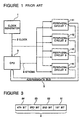
- FIG. 1 there is shown a block diagram of one example of a conventional microcomputer including four peripheral circuits.
- a clock generator 1 generates a clock signal 2, which is supplied unconditionally and commonly to a central processing unit (CPU) 3 and all of four peripheral circuits 41, 42, 43 and 44.
- the clock signal 2 is used as a time reference, on the basis of which the operation order in time and the operation timing of the CPU 3 and the four peripheral circuits 41, 42, 43 and 44 are determined.
- the CPU 3 and the four peripheral circuits 41, 42, 43 and 44 are coupled to each other through an address/data bus 5, and the CPU 3 supplies a strobe signal 6 to all of the four peripheral circuits 41, 42, 43 and 44 for the purpose of controlling a timing of the data read/write operation to the peripheral circuits 41, 42, 43 and 44. Accordingly, the timing of the data read/write operation of the CPU 3 to the peripheral circuits 41, 42, 43 and 44 is determined by this strobe signal 6.
- the conventional general purpose microcomputer includes a plurality of peripheral circuits of various types formed on the single chip, in order to make it possible for the microcomputer to be used in different applications.
- this general purpose microcomputer is used in an actual application system, all of the peripheral circuits formed on the microcomputer chip are not necessarily used.
- unconditional ceaseless application of the clock 2 and the strobe signal 6 to all of the peripheral circuits means that the clock and the strobe signal are applied to the peripheral circuits which are not used in the actual application system, and therefore, an electric power is wastefully consumed.
- Japanese Patent Application Laid-open Publication JP-A-60-195631 has disclosed a data processing system configured to reduce a wasteful electric power consumption.
- This data processing system is constructed to selectively supply a clock signal to peripheral circuits in accordance with a control signal from a CPU.
- the clock signal is applied to each of the peripheral circuits through a corresponding AND gate controlled by the control signal supplied from the CPU.
- control signals to be respectively supplied to the peripheral circuits which are not used in the actual application system are set to "0", so that the application of the clock to these peripheral circuits not to be used is inhibited, and on the other hand, the control signals to be respectively supplied to the peripheral circuits which are used in the actual application system, are set to "1", so that the clock is supplied to these peripheral circuits to be used.
- Japanese Patent Application Laid-open Publication JP-A-61-285521 has proposed a low power consumption microcomputer, which includes a gate for on-off controlling the application of clock to peripheral circuits coupled to the microcomputer, and a clock signal control means for putting the above mentioned gate into an off condition when each peripheral circuit does not actually operate, and for opening the above mentioned gate only when each peripheral circuit actually operates so that the clock is actually supplied to the peripheral circuits.
- the peripheral circuits are controlled to be selectively put into the operating condition.
- a reset signal is applied to a designated peripheral circuit at a designated timing, so that, in a peripheral circuit of the type requiring a clock for the purpose of maintaining an initialized condition after resetting, it is possible to reduce the electric power consumption caused by the clock application after the reset inputting until the peripheral circuit is actually used, whereby a power power consumption computer can be realized.
- Japanese Patent Application Laid-open Publication JP-A-64-86224 shows a stand-by circuit for a microcomputer, which is configured so that, not only a CPU but also peripheral circuits can be selectively stopped when the system is put into a stand-by mode by executing a clock stop instruction in the process of a program execution by a CPU.
- a peripheral hardware controlling circuit is provided, which receives hardware stop information included in the clock stop instruction from the CPU, and selectively supplies a clock stop signal to a plurality of peripheral hardware, for the purpose of reducing the electric power consumption in the stand-by mode.
- the method of reducing the electric power consumption caused by the clock required for maintaining the initialized condition by realizing the reset input in a programmed operation and rendering off the clock used in the peripheral circuits is effective to only limited peripheral circuits required to the clock for maintaining the initialized condition, only when the microcomputer system starts to be used or operated. Therefore, a large advantage cannot be expected if the whole of the microcomputer is considered and if the whole of the use time is considered.
- Another object of the present invention is to provide a one-chip microcomputer having a plurality of peripheral circuits and capable of controlling application of the clock and the strobe signal to the peripheral circuits, without using a program instruction, for making it possible to construct a low power consumption, highly reliable system.
- FIG 2 there is shown a block diagram of a first embodiment of the microcomputer in accordance with the present invention.
- elements similar to those shown in Figure 1 are given the same Reference Numerals, and explanation thereof will be omitted for simplification of description.
- the shown embodiment includes four special external terminals 71, 72, 73 and 74 provided for the four peripheral circuits 41, 42, 43 and 44, respectively.
- Each of the external terminals is used to supply selection information for a corresponding peripheral circuit. For example, when the corresponding peripheral circuit is to be used in an application system, the selection information assumes a logical value "1", and when the corresponding peripheral circuit is not to be used in the application system, the selection information assumes a logical value "0".
- the external terminal 71 is connected to one input of each of four AND gates 91, 101, 111 and 121, each of which has its output connected to the peripheral circuit 41.
- the other input of the AND gate 91 is connected to receive the clock signal 2 from the clock generator 1, and the respective other inputs of the AND gates 101, 111 and 121 are connected to receive three different strobe signals 61, 62 and 63 generated in the CPU 3, respectively.
- the external terminal 72 is connected to one input of each of four AND gates 92, 102, 112 and 122, each of which has its output connected to the peripheral circuit 42.
- the other input of the AND gate 92 is connected to receive the clock signal 2, and the respective other inputs of the AND gates 102, 112 and 122 are connected to receive the strobe signals 61, 62 and 63, respectively.
- the external terminal 73 is connected to one input of each of four AND gates 93, 103, 113 and 123, each of which has its output connected to the peripheral circuit 43.
- the other input of the AND gate 93 is connected to receive the clock signal 2, and the respective other inputs of the AND gates 103, 113 and 123 are connected to receive the strobe signals 61, 62 and 63, respectively.
- the external terminal 74 is connected to one input of each of four AND gates 94, 104, 114 and 124, each of which has its output connected to the peripheral circuit 44.
- the other input of the AND gate 94 is connected to receive the clock signal 2, and the respective other inputs of the AND gate 104, 114 and 124 are connected to receive the strobe signals 61, 62 and 63, respectively.
- the selection information 8 is composed of a first bit 81 indicative of use/non-use of the peripheral circuit 41, a second bit 82 indicative of use/non-use of the peripheral circuit 42, a third bit 83 indicative of use/non-use of the peripheral circuit 43, and a fourth bit 84 indicative of use/non-use of the peripheral circuit 41. Therefore, if the first bit 81 is at the logical value "1", it means use of the peripheral circuit 41, and if the first bit 81 is at the logical value "0", it means non-use of the peripheral circuit 41.
- the respective bits of the selection information 8 can be determined and given by connecting each of the external terminals 71, 72, 73 and 74 to either a voltage supply voltage 13 (Vcc) or ground 14 on an application system board when an application system using the shown microcomputer is constructed by a user.
- Vcc voltage supply voltage 13
- ground 14 ground 14
- the selection information of the logical value "1” is given, and when the external terminal is connected to the ground 14, the selection information of the logical value "0" is given.
- the external terminals 72 and 74 are connected to the voltage supply voltage 13
- the external terminals 71 and 73 are connected to the ground 14.
- the clock 2 generated by the clock generator 1 is supplied to the peripheral circuits 41, 42, 43 and 44 through the AND gates 91, 92, 93 and 94, respectively, which are controlled by the special external terminals 71, 72, 73 and 74, respectively. Therefore, the external terminals set to the logical value "0" keep the corresponding AND gates in a closed condition, so that the clock is not supplied to the corresponding peripheral circuits. On the other hand, the external terminals set to the logical value "1" maintain the corresponding AND gates in an open condition, so that the clock is supplied to the corresponding peripheral circuits .
- the CPU 3 and the respective peripheral circuits 41, 42, 43 and 44 are coupled to each other through the address/data bus 5.
- Each of the peripheral circuits 41, 42, 43 and 44 includes a plurality of registers (not shown) each allocated with an identification address for designating a register. These registers are used for setting an operation condition of the peripheral circuit, for storing an initial data, and for other purposes.
- the strobe signals 61, 62 and 63 generated in the CPU 3 includes an address latch signal 61, a data read signal 62, and a data write signal 63.
- the address latch signal 61 is used for controlling a timing where an address for designating a register in the peripheral circuit is fetched into each peripheral circuit from the address/data bus 5 in the data read/write operation.
- the data read signal 62 is used for controlling a timing where a content of a designated register in the peripheral circuit is read out to the address/data bus 5.
- the data write signal is used for controlling a timing where a designated register in the peripheral circuit is written with a content of the address/data bus 5.
- the address latch signal 61 is supplied to the peripheral circuits 41, 42, 43 and 44 through the AND gates 101, 102, 103 and 104, respectively, which are controlled by the special external terminals 71, 72, 73 and 74, respectively.
- the data read signal 62 is supplied to the peripheral circuits 41, 42, 43 and 44 through the AND gates 111, 112, 113 and 114, respectively, which are also controlled by the special external terminals 71, 72, 73 and 74, respectively.
- the data write signal 63 is supplied to the peripheral circuits 41, 42, 43 and 44 through the AND gates 121, 122, 123 and 124, respectively, which are also controlled by the special external terminals 71, 72, 73 and 74, respectively.
- the external terminals set to the logical value "0" keep the corresponding AND gates in a closed condition, so that none of the strobe signals is supplied to the corresponding peripheral circuits.
- the external terminals set to the logical value "1" maintain the corresponding AND gates in an open condition, so that the strobe signals can be supplied to the corresponding peripheral circuits.
- the external terminals 71 and 73 set to the logical value "0" blocks the corresponding AND gates 91, 101, 111 and 121, and 93, 103, 113 and 123, so that none of the clock 2 and the strobe signals 61, 62 and 63 is supplied to the corresponding peripheral circuits 41 and 43.
- the external terminals 71 and 73 set to the logical value "1" maintain the corresponding AND gates 92, 102, 112 and 122, and 94, 104, 114 and 123 in the open condition, so that the clock 2, the address latch signal 61, the data read signal 62 and the data write signal 63 can be supplied to the corresponding peripheral circuits 42 and 44.
- FIG 4 there is shown a block diagram of a second embodiment of the microcomputer in accordance with the present invention.
- elements similar to those shown in Figure 2 are given the same Reference Numerals, and explanation thereof will be omitted for simplification of description.
- a register 17 having a first bit 171, a second bit 172, a third bit 173 and a fourth bit 174 is provided in place of the external terminals 71, 72, 73 and 74 in the first embodiment.
- the register 17 is coupled to four bits of the address/data bus 5 coupled to an external terminal 16, and controlled through a reset terminal 15 in such a manner that, when a system is reset by activating the reset terminal 15, the first to fourth bits 81, 82, 83 and 84 of the selection information 8 are read through the external terminal 16 and set to the first to fourth bits 171, 172, 173 and 174 of the register 17, respectively.
- the external terminal 16 is used for reading the selection information 8 indicative of the use/non-use of the respective peripheral circuits 41, 42, 43 and 44, only at the time of resetting.
- the external terminal 16 is used as an external address/data terminal for the address/data bus, for making it possible for the CPU 3 to access an external device of the microcomputer, such as a memory, an input/output device and others. Therefore, since the terminal function is multiplexed, a total number of terminals of the microcomputer can be reduced.
- Operation of the second embodiment is the same as that of the first embodiment, excepting for the operation for setting the register 17. Therefore, a further explanation of the operation of the second embodiment will be omitted.
- the second embodiment by determining the selection information 8 to be supplied to the register 17 at the time of resetting the microcomputer, it is possible to select the peripheral circuits to which the clock 2 and the strobe signals 61, 62 and 63 are to be supplied, similarly to the first embodiment.
- the use/non-use of the respective peripheral circuits 41, 42, 43 and 44 determined at the time of the resetting namely, the logical value "1" or "0" of the respective bits 171, 172, 173 and 174 of the register 17 set at the time of the resetting, is not changed until a next resetting.
- the four peripheral circuits are integrated together with the microcomputer.
- the present invention can be applied to microcomputers having more than four peripheral circuits.
- a microcomputer includes ten peripheral circuits (including timers, A/D converters, D/A converters, etc.) and five peripheral circuits of the ten peripheral circuits are not used in an actual application system. If the clock and the strobe signals are inhibited from being supplied to the five peripheral circuits not to be used, the power consumption in connection with the peripheral circuits can be reduced by about 50% in comparison with a case in which the clock and the strobe signals are supplied to all of the ten peripheral circuits integrated on the microcomputer chip. This power consumption reduction effect becomes large if the number or proportion of the peripheral circuits not to be used becomes large.
- the power consumption reduction effect is larger than the case of inhibiting application of only the clock.
- the microcomputer system is constructed to selectively set, through the external terminals, the supply and non-supply of the clock and the strobe signals to the respective peripheral circuits.
- it is constructed to selectively set, only once, the supply and non-supply of the clock and the strobe signals to the respective peripheral circuits, by means of the memory means (such as the register) which is set, at the time of the resetting, on the basis of the use/non-use information of the peripheral circuits. Therefore, since the setting of the supply to the clock and the strobe signals to the respective peripheral circuits cannot be changed by means of a program, it is possible to make zero (0) possibility of a malfunction caused by changing the program. Accordingly, reliability of the microcomputer system can be elevated.
Landscapes
- Engineering & Computer Science (AREA)
- Theoretical Computer Science (AREA)
- Physics & Mathematics (AREA)
- General Engineering & Computer Science (AREA)
- General Physics & Mathematics (AREA)
- Microcomputers (AREA)
- Power Sources (AREA)
Claims (9)
- Mikrocomputer, der folgendes aufweist:wobei die Auswahleinrichtung aus wenigstens einem externen (71, 72, 73, 74) Anschluss des Mikrocomputers gebildet ist.wenigstens eine Zentralverarbeitungseinheit (3),eine Vielzahl von peripheren Schaltungen (41, 42, 43, 44), auf die durch die Zentralverarbeitungseinheit (3) für ein Lesen/Beschreiben der peripheren Schaltungen (41, 42, 43, 44) zugegriffen wird;eine Auswahleinrichtung zum Erzeugen eines Auswahlsignals für jede der peripheren Schaltungen, wobei das Auswahlsignal eine Verwendung oder eine Nichtverwendung der entsprechenden peripheren Schaltung anzeigt; undeine Steuereinrichtung (91 - 94, 101 - 104, 111 - 114, 121- 124) zum Steuern eines Zulassens und eines Verhinderns eines Anlegens eines Taktsignals (2) und eines Tastsignals (61, 62, 63) an jede der peripheren Schaltungen auf der Basis des Auswahlsignals für jede periphere Schaltung,
- Mikrocomputer nach Anspruch 1, wobei der wenigstens eine externe Anschluss in einer Anzahl entsprechend einer Anzahl der Vielzahl von peripheren Schaltungen vorgesehen ist.
- Mikrocomputer nach Anspruch 1, der weiterhin eine Spannungsversorgungsschaltung (14) und eine Erdung (13) aufweist,
wobei Bits einer Auswahlinformation (8) durch selektives Verbinden des wenigstens einen externen Anschlusses (71, 72, 73, 74) mit der Spannungsversorgungsschaltung (14) oder der Erdung (13) geliefert werden. - Mikrocomputer nach Anspruch 1, wobei die Auswahleinrichtung eine Speichereinrichtung (17) zum Halten von Auswahlinformation (8, 171, 172, 173, 174) enthält, die eine Verwendung oder eine Nichtverwendung einer jeweiligen der peripheren Schaltungen (41, 42, 43, 44) anzeigt, wobei die Speichereinrichtung das Auswahlsignal zu einer jeweiligen der peripheren Schaltungen auf der Basis der in der Speichereinrichtung (17) gehaltenen Auswahlinformation (8) zuführt, und wenigstens einen externen Anschluss, der mit der Speichereinrichtung verbunden ist, zum Schreiben der Auswahlinformation in die Speichereinrichtung nur zur Zeit eines Rücksetzens des Mikrocomputers.
- Mikrocomputer nach Anspruch 4, wobei die Speichereinrichtung eine Vielzahl von Bits (171, 172, 173, 174) enthält, wobei die Vielzahl von Bits in einer Anzahl entsprechend einer Anzahl der Vielzahl von peripheren Schaltungen vorgesehen ist.
- Mikrocomputer nach Anspruch 4, der weiterhin eine Einrichtung (15) zum Rücksetzen des Mikrocomputers aufweist, wobei der wenigstens eine externe Anschluss (16) die Auswahlinformation, die die Verwendung oder Nichtverwendung der jeweiligen peripheren Schaltung anzeigt, nur zur Zeit eines Rücksetzens des Mikrocomputers liest.
- Mikrocomputer nach Anspruch 5, der weiterhin einen Adresseri/Daten-Bus (5) zum Koppeln des wenigstens einen externen Anschlusses (16) mit einer jeweiligen der Vielzahl von peripheren Schaltungen und mit der Zentralverarbeitungseinheit aufweist,
wobei der Mikrocomputer weiterhin eine Einrichtung (15) zum Rücksetzen des mit der Speichereinrichtung (17) gekoppelten Mikrocomputers aufweist,
wobei der wenigstens eine externe Anschluss die Auswahlinformation, die die Verwendung oder Nichtverwendung der jeweiligen peripheren Einheit (41, 42, 43, 44) anzeigt, nur zur Zeit eines Rücksetzens des Mikrocomputers liest. - Mikrocomputer nach einem der Ansprüche 1 bis 7, wobei die Steuereinrichtung ein UND-Gatter (91 - 94) zum Empfangen einer ersten Eingabe von dem wenigstens einen externen Anschluss und zum Empfangen einer zweiten Eingabe (2) von einer Takterzeugungsschaltung (1) aufweist, und
wobei das UND-Gatter basierend auf der ersten und der zweiten Eingabe selektiv in einen eines geöffneten Zustands und eines geschlossenen Zustands versetzt wird. - Mikrocomputer nach Anspruch 8, wobei die Steuereinrichtung ein zweites UND-Gatter (101 - 104, 111 - 114, 121 - 124) zum Empfangen einer ersten Eingabe von dem wenigstens einen externen Anschluss und zum Empfangen einer zweiten Eingabe (61, 62, 63) von einer Tastsignal-Erzeugungsschaltung (3) aufweist,
wobei das zweite UND-Gatter basierend auf der ersten und der zweiten Eingabe, die jeweils von dem wenigstens einen externen Anschluss und der Tastsignal-Erzeugungsschaltung selektiv in einen eines geöffneten Zustands und eines geschlossenen Zustands versetzt wird.
Applications Claiming Priority (3)
| Application Number | Priority Date | Filing Date | Title |
|---|---|---|---|
| JP193857/93 | 1993-07-12 | ||
| JP19385793 | 1993-07-12 | ||
| JP5193857A JP2636691B2 (ja) | 1993-07-12 | 1993-07-12 | マイクロコンピュータ |
Publications (2)
| Publication Number | Publication Date |
|---|---|
| EP0634715A1 EP0634715A1 (de) | 1995-01-18 |
| EP0634715B1 true EP0634715B1 (de) | 2002-10-09 |
Family
ID=16314912
Family Applications (1)
| Application Number | Title | Priority Date | Filing Date |
|---|---|---|---|
| EP94110828A Expired - Lifetime EP0634715B1 (de) | 1993-07-12 | 1994-07-12 | Geringem Leistungsverbraucheinchipmikrorechner mit mehreren peripheren Schaltkreisen |
Country Status (5)
| Country | Link |
|---|---|
| US (1) | US5511013A (de) |
| EP (1) | EP0634715B1 (de) |
| JP (1) | JP2636691B2 (de) |
| KR (1) | KR0142033B1 (de) |
| DE (1) | DE69431500T2 (de) |
Families Citing this family (15)
| Publication number | Priority date | Publication date | Assignee | Title |
|---|---|---|---|---|
| US5678065A (en) * | 1994-09-19 | 1997-10-14 | Advanced Micro Devices, Inc. | Computer system employing an enable line for selectively adjusting a peripheral bus clock frequency |
| US5778237A (en) * | 1995-01-10 | 1998-07-07 | Hitachi, Ltd. | Data processor and single-chip microcomputer with changing clock frequency and operating voltage |
| JP3520611B2 (ja) * | 1995-07-06 | 2004-04-19 | 株式会社日立製作所 | プロセッサの制御方法 |
| US5692202A (en) * | 1995-12-29 | 1997-11-25 | Intel Corporation | System, apparatus, and method for managing power in a computer system |
| US5742781A (en) * | 1996-08-09 | 1998-04-21 | Hitachi America, Ltd. | Decoded instruction buffer apparatus and method for reducing power consumption in a digital signal processor |
| US5862393A (en) * | 1996-10-07 | 1999-01-19 | Lxe, Inc. | System for managing power of a computer with removable devices |
| US5918073A (en) * | 1997-06-27 | 1999-06-29 | Advanced Micro Devices, Inc. | System and method for equalizing data buffer storage and fetch rates of peripheral devices |
| JP3633324B2 (ja) | 1998-11-20 | 2005-03-30 | 松下電工株式会社 | マッサージ機 |
| KR100367588B1 (ko) * | 2000-01-24 | 2003-01-10 | 엘지전자 주식회사 | 디지털데이터 플레이어의 상대주소 할당 장치 및 방법 |
| WO2001093051A1 (en) * | 2000-05-30 | 2001-12-06 | Matsushita Electric Industrial Co., Ltd. | Data processing system, and data processing method |
| JP2002041495A (ja) * | 2000-07-21 | 2002-02-08 | Denso Corp | マイクロコンピュータ |
| US7263623B1 (en) * | 2004-03-30 | 2007-08-28 | Altera Corporation | Microprocessor system |
| JP2006172266A (ja) * | 2004-12-17 | 2006-06-29 | Matsushita Electric Ind Co Ltd | ダイレクトメモリアクセスシステム |
| CN103069409B (zh) | 2010-08-26 | 2016-04-06 | 瑞萨电子株式会社 | 数据处理装置和数据处理系统 |
| JP5507694B2 (ja) | 2010-09-02 | 2014-05-28 | ルネサスエレクトロニクス株式会社 | データ処理装置およびデータ処理システム |
Family Cites Families (8)
| Publication number | Priority date | Publication date | Assignee | Title |
|---|---|---|---|---|
| US4694393A (en) * | 1983-06-14 | 1987-09-15 | Sharp Kabushiki Kaisha | Peripheral unit for a microprocessor system |
| US4747041A (en) * | 1983-06-27 | 1988-05-24 | Unisys Corporation | Automatic power control system which automatically activates and deactivates power to selected peripheral devices based upon system requirement |
| JPS60195631A (ja) * | 1984-03-19 | 1985-10-04 | Hitachi Ltd | デ−タ処理装置 |
| JPS61285521A (ja) * | 1985-06-12 | 1986-12-16 | Hitachi Ltd | 低消費電力形コンピユ−タ装置 |
| JPS63126018A (ja) * | 1986-11-17 | 1988-05-30 | Hitachi Ltd | 半導体集積回路 |
| JPS63172345A (ja) * | 1987-01-12 | 1988-07-16 | Canon Inc | スイツチデ−タ入力装置 |
| US4881205A (en) * | 1987-04-21 | 1989-11-14 | Casio Computer Co., Ltd. | Compact electronic apparatus with a refresh unit for a dynamic type memory |
| JPS6454722A (en) * | 1987-08-26 | 1989-03-02 | Matsushita Electric Industrial Co Ltd | Polarizable electrode and manufacture thereof |
-
1993
- 1993-07-12 JP JP5193857A patent/JP2636691B2/ja not_active Expired - Lifetime
-
1994
- 1994-07-11 KR KR1019940016628A patent/KR0142033B1/ko not_active Expired - Fee Related
- 1994-07-12 US US08/274,004 patent/US5511013A/en not_active Expired - Fee Related
- 1994-07-12 DE DE69431500T patent/DE69431500T2/de not_active Expired - Fee Related
- 1994-07-12 EP EP94110828A patent/EP0634715B1/de not_active Expired - Lifetime
Also Published As
| Publication number | Publication date |
|---|---|
| KR0142033B1 (ko) | 1998-07-01 |
| DE69431500T2 (de) | 2003-06-18 |
| KR950003989A (ko) | 1995-02-17 |
| EP0634715A1 (de) | 1995-01-18 |
| DE69431500D1 (de) | 2002-11-14 |
| JPH0728549A (ja) | 1995-01-31 |
| JP2636691B2 (ja) | 1997-07-30 |
| US5511013A (en) | 1996-04-23 |
Similar Documents
| Publication | Publication Date | Title |
|---|---|---|
| EP0634715B1 (de) | Geringem Leistungsverbraucheinchipmikrorechner mit mehreren peripheren Schaltkreisen | |
| US5251304A (en) | Integrated circuit microcontroller with on-chip memory and external bus interface and programmable mechanism for securing the contents of on-chip memory | |
| US5276889A (en) | Microprocessor having built-in synchronous memory with power-saving feature | |
| US5515539A (en) | Apparatus and method for reducing power consumption by peripheral devices after downloading a program therefrom | |
| EP0458614B1 (de) | Speichervorrichtung mit Standby-Funktion | |
| US5408611A (en) | Auto-switching device for CPU logic circuits | |
| JP2003091703A (ja) | カード装置 | |
| US4694393A (en) | Peripheral unit for a microprocessor system | |
| EP0661642A2 (de) | Mikrorechner mit Lesespeicher | |
| US5623687A (en) | Reset configuration in a data processing system and method therefor | |
| KR20070061086A (ko) | 동적 전압 스케일링을 적용한 고효율 프로세서 | |
| EP0374733A1 (de) | Einchip-Mikrorechner mit EPROM | |
| JP2005527037A (ja) | 構成可能なプロセッサ | |
| US7191323B2 (en) | Information processing unit selecting one of reset vector addresses | |
| US5802332A (en) | Single-chip microcomputer and electronic device using the same | |
| US20070180202A1 (en) | Memory controller, semiconductor memory, and memory system | |
| JPS6362778B2 (de) | ||
| JPH0431981A (ja) | ワンチップマイクロコンピュータ | |
| JPH1069336A (ja) | 集積回路 | |
| JPH01181146A (ja) | シングルチップマイクロコンピュータ | |
| CN118860259A (zh) | 存储器数据的读取方法、装置、设备及存储介质 | |
| JP2643803B2 (ja) | マイクロコンピュータ | |
| JPS62286143A (ja) | 半導体記憶装置 | |
| JPH06103106A (ja) | プログラムデバッグ装置 | |
| JPS6239450B2 (de) |
Legal Events
| Date | Code | Title | Description |
|---|---|---|---|
| PUAI | Public reference made under article 153(3) epc to a published international application that has entered the european phase |
Free format text: ORIGINAL CODE: 0009012 |
|
| AK | Designated contracting states |
Kind code of ref document: A1 Designated state(s): DE FR GB |
|
| 17P | Request for examination filed |
Effective date: 19950406 |
|
| 17Q | First examination report despatched |
Effective date: 19991027 |
|
| GRAG | Despatch of communication of intention to grant |
Free format text: ORIGINAL CODE: EPIDOS AGRA |
|
| GRAG | Despatch of communication of intention to grant |
Free format text: ORIGINAL CODE: EPIDOS AGRA |
|
| GRAH | Despatch of communication of intention to grant a patent |
Free format text: ORIGINAL CODE: EPIDOS IGRA |
|
| GRAH | Despatch of communication of intention to grant a patent |
Free format text: ORIGINAL CODE: EPIDOS IGRA |
|
| GRAA | (expected) grant |
Free format text: ORIGINAL CODE: 0009210 |
|
| AK | Designated contracting states |
Kind code of ref document: B1 Designated state(s): DE FR GB |
|
| REG | Reference to a national code |
Ref country code: GB Ref legal event code: FG4D |
|
| REF | Corresponds to: |
Ref document number: 69431500 Country of ref document: DE Date of ref document: 20021114 |
|
| REG | Reference to a national code |
Ref country code: GB Ref legal event code: 732E |
|
| ET | Fr: translation filed | ||
| PGFP | Annual fee paid to national office [announced via postgrant information from national office to epo] |
Ref country code: GB Payment date: 20030709 Year of fee payment: 10 |
|
| PGFP | Annual fee paid to national office [announced via postgrant information from national office to epo] |
Ref country code: FR Payment date: 20030711 Year of fee payment: 10 |
|
| PGFP | Annual fee paid to national office [announced via postgrant information from national office to epo] |
Ref country code: DE Payment date: 20030724 Year of fee payment: 10 |
|
| PLBE | No opposition filed within time limit |
Free format text: ORIGINAL CODE: 0009261 |
|
| STAA | Information on the status of an ep patent application or granted ep patent |
Free format text: STATUS: NO OPPOSITION FILED WITHIN TIME LIMIT |
|
| REG | Reference to a national code |
Ref country code: FR Ref legal event code: TP |
|
| 26N | No opposition filed |
Effective date: 20030710 |
|
| PG25 | Lapsed in a contracting state [announced via postgrant information from national office to epo] |
Ref country code: GB Free format text: LAPSE BECAUSE OF NON-PAYMENT OF DUE FEES Effective date: 20040712 |
|
| PG25 | Lapsed in a contracting state [announced via postgrant information from national office to epo] |
Ref country code: DE Free format text: LAPSE BECAUSE OF NON-PAYMENT OF DUE FEES Effective date: 20050201 |
|
| GBPC | Gb: european patent ceased through non-payment of renewal fee |
Effective date: 20040712 |
|
| PG25 | Lapsed in a contracting state [announced via postgrant information from national office to epo] |
Ref country code: FR Free format text: LAPSE BECAUSE OF NON-PAYMENT OF DUE FEES Effective date: 20050331 |
|
| REG | Reference to a national code |
Ref country code: FR Ref legal event code: ST |