EP0631286A2 - Zur Rauschreduzierung fähige Halbleiterspeicheranordnung - Google Patents
Zur Rauschreduzierung fähige Halbleiterspeicheranordnung Download PDFInfo
- Publication number
- EP0631286A2 EP0631286A2 EP94109804A EP94109804A EP0631286A2 EP 0631286 A2 EP0631286 A2 EP 0631286A2 EP 94109804 A EP94109804 A EP 94109804A EP 94109804 A EP94109804 A EP 94109804A EP 0631286 A2 EP0631286 A2 EP 0631286A2
- Authority
- EP
- European Patent Office
- Prior art keywords
- circuit
- column decoder
- data
- signal
- column
- Prior art date
- Legal status (The legal status is an assumption and is not a legal conclusion. Google has not performed a legal analysis and makes no representation as to the accuracy of the status listed.)
- Withdrawn
Links
Images


Classifications
-
- G—PHYSICS
- G11—INFORMATION STORAGE
- G11C—STATIC STORES
- G11C7/00—Arrangements for writing information into, or reading information out from, a digital store
- G11C7/10—Input/output [I/O] data interface arrangements, e.g. I/O data control circuits, I/O data buffers
- G11C7/1051—Data output circuits, e.g. read-out amplifiers, data output buffers, data output registers, data output level conversion circuits
- G11C7/106—Data output latches
-
- G—PHYSICS
- G11—INFORMATION STORAGE
- G11C—STATIC STORES
- G11C7/00—Arrangements for writing information into, or reading information out from, a digital store
- G11C7/10—Input/output [I/O] data interface arrangements, e.g. I/O data control circuits, I/O data buffers
- G11C7/1051—Data output circuits, e.g. read-out amplifiers, data output buffers, data output registers, data output level conversion circuits
-
- G—PHYSICS
- G11—INFORMATION STORAGE
- G11C—STATIC STORES
- G11C8/00—Arrangements for selecting an address in a digital store
- G11C8/18—Address timing or clocking circuits; Address control signal generation or management, e.g. for row address strobe [RAS] or column address strobe [CAS] signals
-
- G—PHYSICS
- G11—INFORMATION STORAGE
- G11C—STATIC STORES
- G11C7/00—Arrangements for writing information into, or reading information out from, a digital store
- G11C7/06—Sense amplifiers; Associated circuits, e.g. timing or triggering circuits
Definitions
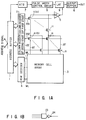
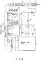
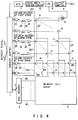
- the rise of the decode signal CDEC1 is completed before the rise of the selection signal supplied from the column decoder 122 of the lower hierarchy, which controls access time, is completed, that is, before time T2 when the decode signal CDEC2 is determined, and the decode signal CDEC1 is thus determined at time T1. Therefore, access time is not influenced at all.
- An EPROM, a NOR flash memory, an MROM, or the like can be applied to the memory circuit of the present invention.
Applications Claiming Priority (2)
| Application Number | Priority Date | Filing Date | Title |
|---|---|---|---|
| JP15469093A JP3130705B2 (ja) | 1993-06-25 | 1993-06-25 | 半導体メモリ回路 |
| JP154690/93 | 1993-06-25 |
Publications (2)
| Publication Number | Publication Date |
|---|---|
| EP0631286A2 true EP0631286A2 (de) | 1994-12-28 |
| EP0631286A3 EP0631286A3 (de) | 1995-03-08 |
Family
ID=15589809
Family Applications (1)
| Application Number | Title | Priority Date | Filing Date |
|---|---|---|---|
| EP94109804A Withdrawn EP0631286A3 (de) | 1993-06-25 | 1994-06-24 | Zur Rauschreduzierung fähige Halbleiterspeicheranordnung. |
Country Status (4)
| Country | Link |
|---|---|
| US (1) | US5457661A (de) |
| EP (1) | EP0631286A3 (de) |
| JP (1) | JP3130705B2 (de) |
| KR (1) | KR0139871B1 (de) |
Cited By (1)
| Publication number | Priority date | Publication date | Assignee | Title |
|---|---|---|---|---|
| WO1998020495A1 (en) * | 1996-11-04 | 1998-05-14 | Micron Technology, Inc. | Staggered row line firing in a single ras cycle |
Families Citing this family (16)
| Publication number | Priority date | Publication date | Assignee | Title |
|---|---|---|---|---|
| JP3275554B2 (ja) * | 1994-08-09 | 2002-04-15 | ヤマハ株式会社 | 半導体記憶装置 |
| JPH08101669A (ja) * | 1994-09-30 | 1996-04-16 | Semiconductor Energy Lab Co Ltd | 表示装置駆動回路 |
| KR0166046B1 (ko) * | 1995-10-06 | 1999-02-01 | 김주용 | 계층적 비트라인 구조를 갖는 반도체 메모리 장치 |
| US5757718A (en) * | 1996-02-28 | 1998-05-26 | Nec Corporation | Semiconductor memory device having address transition detection circuit for controlling sense and latch operations |
| EP0801393B1 (de) * | 1996-04-09 | 2004-03-10 | STMicroelectronics S.r.l. | Schaltung zur Bestimmung der vollständigen Aufladung einer generischen Bitleitung, insbesondere für nichtflüchtige Speicher |
| JP4334038B2 (ja) * | 1998-08-28 | 2009-09-16 | 株式会社ルネサステクノロジ | 半導体記憶装置 |
| KR100576450B1 (ko) * | 1998-12-28 | 2006-08-23 | 주식회사 하이닉스반도체 | 동기식 메모리의 데이타 액세스장치 |
| JP3779480B2 (ja) | 1999-02-10 | 2006-05-31 | Necエレクトロニクス株式会社 | 半導体記憶装置 |
| KR100388214B1 (ko) * | 1999-06-30 | 2003-06-19 | 주식회사 하이닉스반도체 | 펄스워드라인신호 발생기 |
| JP4803887B2 (ja) * | 2001-02-26 | 2011-10-26 | ローム株式会社 | シリアルメモリ装置 |
| JP3753040B2 (ja) | 2001-09-25 | 2006-03-08 | 住友電気工業株式会社 | 光ファイバ融着接続部の加熱方法および加熱装置 |
| KR100515055B1 (ko) * | 2002-12-12 | 2005-09-14 | 삼성전자주식회사 | 모든 칼럼 선택 트랜지스터들을 선택할 수 있는 칼럼 프리디코더를 갖는 플레쉬 메모리 장치와 그 스트레스 테스트방법 |
| US7082064B2 (en) * | 2004-01-29 | 2006-07-25 | Micron Technology, Inc. | Individual I/O modulation in memory devices |
| KR100827657B1 (ko) | 2006-09-05 | 2008-05-07 | 삼성전자주식회사 | 반도체 메모리 장치. |
| JP5339541B2 (ja) * | 2007-05-25 | 2013-11-13 | マーベル ワールド トレード リミテッド | ビット線デコーダ及び集積回路 |
| WO2015087413A1 (ja) * | 2013-12-11 | 2015-06-18 | ユニサンティス エレクトロニクス シンガポール プライベート リミテッド | 半導体装置 |
Citations (2)
| Publication number | Priority date | Publication date | Assignee | Title |
|---|---|---|---|---|
| EP0314180A2 (de) * | 1987-10-28 | 1989-05-03 | Kabushiki Kaisha Toshiba | Nichtflüchtiger Halbleiterspeicher mit Belastungsprüfschaltung |
| EP0543269A2 (de) * | 1991-11-20 | 1993-05-26 | Fujitsu Limited | Generator zum Folgen eines Impulses und RAM mit Generator zum Folgen eines Vorladungsimpuls |
Family Cites Families (2)
| Publication number | Priority date | Publication date | Assignee | Title |
|---|---|---|---|---|
| JPS6124091A (ja) * | 1984-07-12 | 1986-02-01 | Nec Corp | メモリ回路 |
| US5313422A (en) * | 1991-05-29 | 1994-05-17 | Texas Instruments Incorporated | Digitally controlled delay applied to address decoder for write vs. read |
-
1993
- 1993-06-25 JP JP15469093A patent/JP3130705B2/ja not_active Expired - Fee Related
-
1994
- 1994-06-23 KR KR1019940014417A patent/KR0139871B1/ko not_active IP Right Cessation
- 1994-06-23 US US08/264,775 patent/US5457661A/en not_active Expired - Lifetime
- 1994-06-24 EP EP94109804A patent/EP0631286A3/de not_active Withdrawn
Patent Citations (2)
| Publication number | Priority date | Publication date | Assignee | Title |
|---|---|---|---|---|
| EP0314180A2 (de) * | 1987-10-28 | 1989-05-03 | Kabushiki Kaisha Toshiba | Nichtflüchtiger Halbleiterspeicher mit Belastungsprüfschaltung |
| EP0543269A2 (de) * | 1991-11-20 | 1993-05-26 | Fujitsu Limited | Generator zum Folgen eines Impulses und RAM mit Generator zum Folgen eines Vorladungsimpuls |
Cited By (1)
| Publication number | Priority date | Publication date | Assignee | Title |
|---|---|---|---|---|
| WO1998020495A1 (en) * | 1996-11-04 | 1998-05-14 | Micron Technology, Inc. | Staggered row line firing in a single ras cycle |
Also Published As
| Publication number | Publication date |
|---|---|
| KR0139871B1 (ko) | 1998-08-17 |
| US5457661A (en) | 1995-10-10 |
| KR950002074A (ko) | 1995-01-04 |
| EP0631286A3 (de) | 1995-03-08 |
| JP3130705B2 (ja) | 2001-01-31 |
| JPH07141869A (ja) | 1995-06-02 |
Similar Documents
| Publication | Publication Date | Title |
|---|---|---|
| US5457661A (en) | Semiconductor memory device having a delay circuit for controlling access time | |
| JP3652812B2 (ja) | 不揮発性メモリ装置及びその読出方法 | |
| US5058066A (en) | Output buffer precharge circuit for DRAM | |
| US5479374A (en) | Semiconductor memory device employing sense amplifier control circuit and word line control circuit | |
| US4445204A (en) | Memory device | |
| US5214605A (en) | Automatic erasing optimization circuit for an electrically erasable and programmable semiconductor memory and method thereof | |
| JPH08321196A (ja) | 集積回路形式メモリの読出のための電流検出回路 | |
| US4967394A (en) | Semiconductor memory device having a test cell array | |
| US6906952B2 (en) | Nonvolatile semiconductor memory device and data writing method therefor | |
| US5719812A (en) | Semiconductor memory including bit line reset circuitry and a pulse generator having output delay time dependent on type of transition in an input signal | |
| US5657269A (en) | Semiconductor storage device having address-transition detecting circuit and sense-determination detecting circuit | |
| US5160861A (en) | Circuit for controlling the output of a sense amplifier | |
| US4901281A (en) | Semiconductor memory device having two column transfer gate transistor groups independently provided for a sense amplifier and a programmed circuit | |
| EP0500958A1 (de) | Initialisierungsschaltung und halbleiteranordnung mit solcher schaltung | |
| WO1994007243A1 (en) | High speed memory sense amplifier with noise reduction | |
| US6728125B2 (en) | Bit line selection circuit having hierarchical structure | |
| US4858188A (en) | Semiconductor memory with improved write function | |
| US5270978A (en) | Nonvolatile memory circuit | |
| US6717444B2 (en) | Low power latch sense amplifier | |
| US6195297B1 (en) | Semiconductor memory device having pull-down function for non-selected bit lines | |
| US4815036A (en) | Programmable logic array having an on/off sense function | |
| US5812460A (en) | Nonvolatile semiconductor memory device having test circuit for testing erasing function thereof | |
| US5886941A (en) | Address decoder and address decoding method | |
| KR100205788B1 (ko) | 불휘발성 반도체 메모리 장치 | |
| KR100555521B1 (ko) | 두 번 이상 샘플링하는 감지 증폭기를 구비하는 반도체 장치 및 반도체 장치의 데이터 판독 방법 |
Legal Events
| Date | Code | Title | Description |
|---|---|---|---|
| PUAI | Public reference made under article 153(3) epc to a published international application that has entered the european phase |
Free format text: ORIGINAL CODE: 0009012 |
|
| 17P | Request for examination filed |
Effective date: 19940624 |
|
| AK | Designated contracting states |
Kind code of ref document: A2 Designated state(s): DE FR GB |
|
| PUAL | Search report despatched |
Free format text: ORIGINAL CODE: 0009013 |
|
| AK | Designated contracting states |
Kind code of ref document: A3 Designated state(s): DE FR GB |
|
| 17Q | First examination report despatched |
Effective date: 19980313 |
|
| STAA | Information on the status of an ep patent application or granted ep patent |
Free format text: STATUS: THE APPLICATION IS DEEMED TO BE WITHDRAWN |
|
| 18D | Application deemed to be withdrawn |
Effective date: 19980724 |