-
The present invention relates to a semiconductor memory circuit and, more specifically, to a semiconductor memory circuit having a function of latching data until the its subsequent data is determined in a sense amplifier in order to stably read out the data.
-
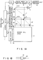
FIGS. 1A and 1B are circuit diagrams showing a readout system of a conventional nonvolatile memory. In the circuit of FIG. 1A, a bit line (column selection line) is selected as follows. Address signals are supplied from an address pin to a column decoder 21 of first stage and a column decoder 22 of second stage through an address buffer 1. In each of the column decoders 21 and 22, a NAND gate 23 and an inverter 24 are connected in series, as shown in FIG. 1B, and then connected to the gates of selecting transistors 11. The first-stage column decoder 21 outputs a first selection signal SS1 and the second-stage column decoder 22 outputs a second selection signal SS2 to turn on the selecting transistors 11(a) and 11(b), respectively. Thus, one bit line BT is selected from a memory cell array 3. In contrast, an address signal is supplied to a row selection circuit 4 through the address buffer 1, and one word line (row selection line) WL is selected from the memory cell array 3. Data of a memory cell at the crossing point of the selected bit and word lines is transmitted to a sense amplifier 5 via the selecting transistors 11(a) and 11(b). The sense amplifier 5 determines whether the data is "0" or "1", and outputs it via a buffer circuit 6.
-
While the sense amplifier 5 is sensing data, an unstable state influences the buffer circuit 6 or data to be output. More specifically, the following drawback arises. In the memory cell selection process, the currently-selected bit and word lines are not changed to new ones instantaneously, but there occurs a difference in time between the selection of the current bit and word lines and that of the new ones. Just then, data of a memory cell other than a desired memory cell is read. If the read data is determined as data opposite to desired data by the sense amplifier, it is reversed. Thus, a large-sized transistor in the buffer circuit 6 repeats turning on and turning off until the data is determined by the sense amplifier, which is likely to be a noise source of a power line. The noise source adversely affects access time.
-
To eliminate the above drawback, an ATD (address transition detector) circuit 7 for detecting a transition of an address signal and generating a pulse is employed to latch data until its subsequent data is determined by the sense amplifier and then output the data as readout data. More specifically, the ATD circuit 7 receives an address signal from the address buffer and generates a pulse. The pulse is controlled by a pulse width control circuit 8 so as to have a width required for determining data by the sense amplifier 5. A latch circuit 9 latches data to be read out in accordance with the width of the pulse. When an address signal is changed to a new one, the latch circuit 9 still latches old data, which is obtained before the address signal is changed, by the functions of the ATD circuit 7 and pulse width control circuit 8. When new data is determined by the sense amplifier 5, the pulse supplied to the latch circuit 9, and the latch circuit 9 transfers the new data to the buffer circuit 6 in response to the new address signal. The new data is then output as new readout data.
-
In the foregoing circuit arrangement, since both the buffer circuit 6 and readout data are stable even while the sense amplifier 5 is sensing its subsequent data, noise can be eliminated, with the result that an access operation can be performed at high speed.
-
If, however, data of the sense amplifier 5 is reversed before its preceding data is latched in response to the pulse generated from the ATD circuit 7, data opposite to the preceding data is latched, which causes noise. The pulse transmitted to the latch circuit 9 has an unignorable delay due to gate delays of the ATD circuit 7 and pulse width control circuit 8 or wiring delays caused by wiring resistance and wiring capacity. Therefore, the column decoders 21 and 22 are operated at high speed, and the bit lines (column selection lines) are switched quickly. If, in this case, data of a selected memory cell is opposite to its preceding data to be latched, the opposite data is input to the latch circuit 9 through the sense amplifier 5 before the pulse is input thereto. Thus, the opposite data is latched.
-
There may be a case where, when a row selection signal is switched very quickly and a row selection line is changed accordingly, data of a memory cell acquired by this change is opposite to its preceding data, and the reversed data of the sense amplifier rises earlier than the pulse from the ATD does. In a nonvolatile memory, generally, the word lines are connected to the gates of a plurality of memory cells and, even though a word line selection signal is changed very quickly, it takes time to increase the gate potential of the memory cells over the threshold value of the "1" data cells so that data can be read out. Actually, in most cases, access time is controlled by the rise of word lines. Therefore, it is bit lines (column selection lines) that are switched quickly.
-
As has been known conventionally, in a nonvolatile memory, "1" data is read out very quickly in the column direction. The reason is as follows. A nonselected bit line of about 0 V corresponds to the "1" data due to discharge from the drain junction of memory cells. When "1" data is read out through the bit line of 0 V, the sense amplifier is to read out the "1" data simply because a bit line is switched. All signals supplied to address pins are likely to be changed, depending upon where a selected cell is located, and all address buffers are operated to cause a large current to flow in the total of chips. If the large current flows, the potential at the power line is lowered instantaneously. If the control circuit 8 is weaker to noise than the sense amplifier 5, the rise of a pulse signal deteriorates and the timing at which data is lathced is delayed. If, furthermore, the latch circuit 9 is located far away from the ATD circuit 7 for generating a pulse, the wiring resistance and wiring capacity are increased to an unignorable extent, with the result that the timing at which data is latched is delayed more and more.
-
When the foregoing drawbacks occur, "1" data, which is read out quickly in a "1" data read mode, is latched.
-
In short, the conventional memory device has the following drawback. When an address signal is changed to a new one, if data of the sense amplifier is reversed in response to the new address signal before the preceding data, which is obtained before the address signal is changed, is latched in response to a pulse generated from the ATD circuit, the reversed data is latched, which causes noise.
-
It is accordingly an object of the present invention to provide a semiconductor memory circuit which operates a sense amplifier in a read mode, latches data before its subsequent data is reversed, and exercises no adverse influence on access time, under any condition.
-
To attain the above object, there is provided a semiconductor memory circuit, comprising:
a memory cell array including a plurality of memory cells;
a plurality of column selection lines constituting connection lines extending in a column direction of the memory cell array and divided into predetermined hierarchies by providing selecting transistors;
a plurality of row selection lines constituting connection lines extending in a row direction of the memory cell array;
a sense amplifier for receiving data from the memory cells through the column selection lines and determining the data;
an address buffer circuit for converting an externally input address signal to an internal signal;
data holding means for detecting a transition of the internal signal supplied from the address buffer circuit to generate a pulse signal, and preventing data of the memory cell from changing in response to the pulse signal in order to hold readout data precedent to the data for a period of time from when the address signal is converted to the internal signal until when the data of the memory cell is determined by the sense amplifier;
a row decoder for selecting the row selection lines in response to the internal signal supplied from the address buffer circuit;
a column decoder arranged for each of the predetermined hierarchies, for selecting the column selection lines through the selecting transistors in response to the internal signal supplied from the address buffer circuit; and
delay means provided in the column decoder, for decreasing a selection speed of the selecting transistors belonging to at least an upper one of the predetermined hierarchies.
-
According to the circuit arrangement described above, the delay means delays a signal supplied from a column decoder of the upper hierarchy, which causes data of a memory cell to be output earlier than a pulse signal supplied to the data holding means, and the timing at which the column selection line connected to the sense amplifier is changed, is delayed. Therefore, a period of time during which the sense amplifier is sensing data, is lengthened and, during this period, the latch circuit 9 is operated to latch the preceding data. Furthermore, the rise of the signal delayed by the delay means is not later than that of a signal output from the column decoder of the lower hierarchy, which controls access speed. The access speed is not therefore decreased.
-
This invention can be more fully understood from the following detailed description when taken in conjunction with the accompanying drawings, in which:
- FIG. 1A is a circuit diagram of a readout system of a conventional nonvolatile memory circuit;
- FIG. 1B is a circuit diagram of part of the readout system shown in FIG. 1A;
- FIG. 2 is a circuit diagram showing an arrangement of a readout system of a nonvolatile semiconductor memory circuit according to a first embodiment of the present invention;
- FIG. 3 is a timing chart of respective components, showing an operation of the memory circuit of FIG. 2;
- FIG. 4 is a circuit diagram showing an arrangement of a readout system of a nonvolatile semiconductor memory circuit according to a second embodiment of the present invention;
- FIG. 5 is a circuit diagram showing an arrangement of a readout system of a nonvolatile semiconductor memory circuit according to a third embodiment of the present invention; and
- FIG. 6 is a circuit diagram showing an arrangement of a readout system of a nonvolatile semiconductor memory circuit according to a fourth embodiment of the present invention.
-
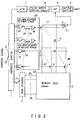
FIG. 2 is a circuit diagram showing an arrangement of a readout system of a nonvolatile semiconductor memory according to a first embodiment of the present invention. In FIG. 2, the same components as those in FIG. 1 are denoted by the same reference numerals. A plurality of memory cells (not shown) are arranged in matrix in a memory cell array 3. The respective column selection lines (bit lines) BT of the memory cell array 3 hierarchically extend through selecting transistors 11 to be structured as a tree. The column decoder is hierarchically divided into a column decoder 12 of first stage and a column decoder 122 of second stage. The row selection lines (word lines) WL of the memory cell array 3 are controlled by a row decoder 4.
-
The readout system includes an ATD circuit 7 for generating a pulse by detecting a transition of an address signal, a pulse width control circuit 8 for controlling the pulse generated from the ATD circuit 7 so as to have a width necessary for determining data in a sense amplifier 5, a latch circuit 9 for latching the data in accordance with the pulse width obtained from the pulse width control circuit 8, and an output buffer 6 for receiving the data from the latch circuit 9 and outputting it as readout data.
-
In the first-stage column decoder 121 of the upper hierarchy, the number of selecting transistors 11 is small, and a signal rises at very high speed. In the second-stage column decoder 122 of the lower hierarchy, the number of selecting transistors 11 is large. In the first embodiment, therefore, the first-stage column decoder 121 is provided with a signal delay means so that the bit line selection speed of the column decoder 121 becomes close to that of the column decoder 122. In other words, the transmission of signals to the selecting transistors is controlled by actively arranging a signal delay means in the first-stage column decoder 121. In general, a delay circuit is added to a column decoder from which a signal is transmitted to a column selection line (bit line) at higher speed than the normal speed in order to make the speed coincident with a speed for determining a decode signal of another column decoder from which a signal is transmitted to a column selection line at the normal speed. Access time is determined based on the normal speed.
-
While the second-stage column decoder 122 has the same structure as that of the column decoder shown in FIG. 1B, the first-stage column decoder 121 includes a NAND gate 23, a NOR gate 25, and two inverters 24 connected in series between the gates 23 and 25. The NOR gate 25 receives both an output signal of the NAND gate 23 and a signal generated by delaying the output signal of the gate 23 by the two inverters 24.
-
In the foregoing circuit arrangement of the readout system, since a selection signal supplied to the column selection line causes data of a memory cell to be output earlier than a pulse signal generated from the ATD circuit 7, the selection signal is delayed by the inverters 24 constituting a delay circuit and accordingly the timing of transition between the column selection lines connected to the sense amplifier 5 is delayed. Therefore, a period of time during which the sense amplifier 5 is sensing the data is lengthened and, during this period, the latch circuit 9 is operated to latch the preceding data.
-
It is because a selection signal supplied from the upper hierarchy, that is, a decode signal supplied from the first-stage column decoder 121 that data of a memory cell is output earlier than a pulse signal is transmitted from the ATD circuit 7 to the latch circuit 9. Therefore, the delay circuit is added to the first-stage column decoder 121. Access time is not lengthened unless the rise of the selection signal delayed by the delay circuit is later than determination of a selection signal supplied from the lower hierarchy which controls the access time, that is, determination of a decode signal supplied from the second-stage column decoder 122.
-
FIG. 3 is a timing chart of the respective components showing an operation of the readout system of FIG. 2. In response to a signal ATD of the ATD circuit 7 for detecting the transition of address signal ADRS, the pulse width control circuit 8 outputs a latch pulse signal LATP. The latch circuit 9 receives a data signal AMP from the sense amplifier 5 in response to the signal LATP. A decode signal CDEC of the first-stage column decoder 121 and a decode signal CDEC2 of the second-stage column decoder 122 are supplied to the gates of their corresponding selecting transistors 11. Since the number of selecting transistors 11 for the column decoder 122 is larger than that of selecting transistors 11 for the column decoder 121, the rising speed of the decode signal CDEC2 is lower than that of the decode signal CDEC1 in view of CR time constant. If the column decoder 121 does not include the inverters 24 of the delay circuit, the rise of the decode signal CDEC1 is completed before the latch pulse signal LATP rises, as indicated by dotted line RS in FIG. 3, and it is likely that undetermined data will be supplied to the sense amplifier 5 and then latched by the latch circuit 9. The circuit of the present invention is so improved that the inverters 24 cause the decode signal CDEC1 to be always determined after time T0 when the rise of the latch pulse signal LATP is completed. Furthermore, the rise of the decode signal CDEC1 is completed before the rise of the selection signal supplied from the column decoder 122 of the lower hierarchy, which controls access time, is completed, that is, before time T2 when the decode signal CDEC2 is determined, and the decode signal CDEC1 is thus determined at time T1. Therefore, access time is not influenced at all.
-
According to the above circuit arrangement, the inverters 24 are capable of delaying the rise timing of an output signal of the first-stage column decoder 121, and the NOR gate 25 allows access time to be equal to that of the circuit shown in FIG. 1, without delaying the fall timing of the output signal of the column decoder 121. Consequently, a problem of noise, which causes access time to be lengthened, can be eliminated.
-
In the first embodiment described above, two column decoders are formed. However, three or more column decoders can be formed and, in this case, too, the column decoders excluding the column decoder of the lowermost hierarchy can be provided with delay circuits in order to make their bit line selection timings close to that of the column decoder of the lowermost hierarchy which controls access time.
-
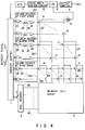
FIG. 4 is a circuit diagram showing an arrangement of a readout system of a nonvolatile semiconductor memory circuit according to a second embodiment of the present invention. In FIG. 4, the same components as those in FIG. 2 are denoted by the same reference numerals. The respective column selection lines (bit lines) BT of the memory cell array 3 extend through selecting transistors 11 and are structured as a tree of three hierarchies, and a column decoder is divided into three column decoders ―a column decoder 221 of first stage, a column decoder 222 of second stage, and a column decoder 223 of third stage―corresponding to the three hierarchies. In FIG. 4, for example, the number of bit lines belonging to the first-stage column decoder 221 is 8, the number of bit lines belonging to the second-stage column decoder 222 is 64 because 8 bit lines are connected to each of 8 bit lines of the column decoder 221, and the number of bit lines belonging to the third-stage column decoder 223 is 512 because 8 bit lines are connected to each of 64 bit lines of the column decoder 222.
-
In the second embodiment, the number of selecting transistors 11 of each of the first- and second- stage column decoders 221 and 222 is smaller than that of selecting transistors 11 of the third-stage column decoder 223, and the rising speed of a signal output from each of the column decoders 221 and 22 is higher than that of a signal output from the column decoder 223. Therefore, the first- and second- stage column decoders 221 and 222 are provided with signal delay circuits in order to make the bit line selection speed of each of the column decoders 221 and 22 close to that of the column decoder 223.
-
While the arrangement of the third-stage column decoder 223 is the same as that of the column decoder shown in FIG. 1B, each of the first- and second- stage column decoders 221 and 222 includes a NAND gate 23, a NOR gate 25, and inverters 24 connected in series between the gates 23 and 25. The NOR gate 25 receives both an output signal of the NAND gate 23 and a signal generated by delaying the output signal of the gate 23 by the inverters 24. The circuit arrangement of the second embodiment is capable of resolving a problem of noise, without having any influence on access time, as that of the first embodiment shown in FIG. 2.
-
FIG. 5 is a circuit diagram showing an arrangement of a readout system of a nonvolatile semiconductor memory circuit according to a third embodiment of the present invention. In FIG. 5, the same components as those in FIG. 4 are denoted by the same reference numerals. The structure of FIG. 5 differs from that of FIG. 4 in a delay circuit of a column decoder 321 of first stage. More specifically, the column decoder 321 includes a NAND gate 23, a NOR gate 25, and four inverters 24 connected in series between the gates 23 and 25, and the NOR gate 25 receives both an output signal of the NAND gate 23 and a signal generated by delaying the output signal of the gate 23 by the four inverters 24.
-
As in the second embodiment shown in FIG. 4, the first- and second- stage column decoders 321 and 322 include inverters 24 serving as a signal delay circuit in order to make their bit line selection timings close to that of the third-stage column decoder 323. In the third embodiment, however, the inverters are arranged so as to reflect the number of selecting transistors 11 more strictly. According to the arrangement of the third embodiment, it is possible that the bit line selection speed of the first-stage column decoder 321 is lower than that of the second-stage column decoder 322. Needless to say, the bit line selection speed of the first-stage column decoder 321 has to be higher than that of the third-stage column decoder 323 which controls access time, so as not to exercise any influence on the access time. In the third embodiment, too, a problem of noise can be eliminated without any influence on access time.
-
FIG. 6 is a circuit diagram showing an arrangement of a readout system of a nonvolatile semiconductor memory circuit according to a fourth embodiment of the present invention. Taking into consideration the circuit arrangement of FIG. 5, in the fourth embodiment, a plurality of column decoders 42n, 42n+1 (n = 1, 2, 3, ...) corresponding to a plurality of hierarchies, can be constituted in accordance with selecting transistors 11 which are structured as a tree of the hierarchies. In order to reflect the number of selecting transistors 11 for each of the hierarchies, delay circuits DL1 to DLn are arranged in the column decoders 421 to 42n, respectively. Of course, the bit line selection timing of the first-stage column decoder 421 has to be earlier than that of the column decoder 42n+1 of the lowest hierarchy to exercise no influence on access time.
-
As described above, according to the present invention, the delay circuit of the column decoder of the upper hierarchy causes a signal from the ATD circuit to always operate the latch circuit earlier than the timing of transition of data in the sense amplifier, thereby to latch the preceding data before the data of the sense amplifier is reversed. Since, furthermore, the rise of a signal delayed by the delay circuit is not later than that of a signal output from the column decoder of the lower hierarchy, which controls access speed, the access speed is not decreased. Consequently, the semiconductor memory circuit of the present invention is capable of eliminating a problem of noise which causes the access speed to decrease.
-
An EPROM, a NOR flash memory, an MROM, or the like can be applied to the memory circuit of the present invention.