EP0617458A2 - Verfahren zum Ätzen von Halbleitern und Ätzlösung dafür - Google Patents
Verfahren zum Ätzen von Halbleitern und Ätzlösung dafür Download PDFInfo
- Publication number
- EP0617458A2 EP0617458A2 EP93120476A EP93120476A EP0617458A2 EP 0617458 A2 EP0617458 A2 EP 0617458A2 EP 93120476 A EP93120476 A EP 93120476A EP 93120476 A EP93120476 A EP 93120476A EP 0617458 A2 EP0617458 A2 EP 0617458A2
- Authority
- EP
- European Patent Office
- Prior art keywords
- layer
- etching
- ingaas
- algaas
- gaas
- Prior art date
- Legal status (The legal status is an assumption and is not a legal conclusion. Google has not performed a legal analysis and makes no representation as to the accuracy of the status listed.)
- Ceased
Links
Images


Classifications
-
- H10P50/646—
Definitions
- the present invention relates to etching solution used for etching semiconductor and etching method using this etching solution.
- FIG. 17 is a cross sectional view illustrating a semiconductor device to which an etching is carried out using the prior art etching solution.
- reference numeral 1 designates an n type AlGaAs layer.
- An n+ type GaAs layer 2 is disposed on the n type AlGaAs layer 1.
- a photoresist 3 is disposed on the n+ type GaAs layer 2.
- Reference character d designates an etching depth to that the n+ type GaAs layer 2 is etched and reference character ⁇ d designates an over etching depth to that the n type AlGaAs layer 1 is excessively etched.
- Figure 18 is a cross sectional view illustrating an HEMT (high electron mobility transistor) produced by employing a prior art etching solution.
- Reference numeral 4 designates a GaAs substrate.
- An i type GaAs layer 5 is disposed on the GaAs substrate 4.
- An i type InGaAs layer 6 is disposed on the i type GaAs layer 5.
- the n type AlGaAs layer 1 and the n+ type GaAs layer 2 are disposed on the i type GaAs layer 5 in figure 17.
- a drain electrode 7 and a source electrode 8 are disposed on the n+ type GaAs layer 2.
- the threshold voltage V th of this HEMT is represented by the following formula (1):
- the etching speeds of the n+ type GaAs layer 2 and the n type AlGaAs layer 1 are both about 30 nm/min., and therefore, when this etching solution is applied to producing a gate recess of HEMT, there arises a variation ⁇ d in the recess depth (d) in figures 17 and 18.
- the thickness W of the AlGaAs layer 1 which appears in the formula (1) defining the threshold voltage V th of the HEMT is determined by the recess depth (d)
- the thickness W of the AlGaAs layer 1 varies when the recess depth (d) varies as described above, occurring a variation in the threshold voltage V th , finally resulting in a variation in the characteristics of the HEMT.
- the prior art etching solution does not have selectivity for the difference of material as described above, and when it is used in producing a heterostructure device, a precise control was difficult.
- an etching solution comprises a mixed solution of organic acid and hydrogen peroxide mixed in a volume ratio of 1:1 to 200:1 with basic material being added thereto so as to produce a pH of 6.0 to 8.0.
- An etching method comprises etching a GaAs layer selectively with an AlGaAs layer for a layer structure comprising the AlGaAs layer and the GaAs layer produced thereon. This may be applied to a layer structure comprising an n type AlGaAs layer and an n+ type GaAs layer produced thereon, of a HEMT.
- an etching solution comprises a mixed solution of organic acid and hydrogen peroxide mixed in a volume ratio of 1:1 to 200:1 with basic material being added thereto so as to produce a pH of above 6.0.
- An etching method comprises etching a GaAs layer selectively with an InGaAs layer for a layer structure comprising the InGaAs layer and the GaAs layer produced thereon. This may be applied to a layer structure comprising an n type InGaAs layer and an n+ type GaAs layer produced thereon, of a MESFET.
- an etching solution comprises a mixed solution of organic acid and hydrogen peroxide mixed in a volume ratio of 1:1 to 200:1 with basic material being added thereto so as to produce a pH of above 7.0.
- An etching method comprises etching an AlGaAs layer selectively with an InGaAs layer for a layer structure comprising the InGaAs layer and the AlGaAs layer produced thereon. This may be applied to a layer structure comprising a p+ type InGaAs base layer and an n type AlGaAs layer produced thereon, of a HEMT.
- an etching solution comprises a mixed solution of organic acid and hydrogen peroxide mixed in a volume ratio of 1:1 to 200:1 with basic material being added thereto so as to produce a pH of 4.5 to 5.5.
- An etching method comprises etching an InGaAs layer selectively with an AlGaAs layer for a layer structure comprising the InGaAs layer and the AlGaAs layer produced thereon. This may be applied to a layer structure comprising an n type AlGaAs emitter layer and an n type InGaAs emitter layer produced thereon, of an HBT.
- an etching solution comprises a mixed solution of organic acid and hydrogen peroxide mixed in a volume ratio of 1:1 to 200:1 with basic material being added thereto so as to produce a pH of 4.5 to 5.5.
- An etching method comprises etching an InGaAs layer selectively with a GaAs layer for a layer structure comprising the GaAs layer and the InGaAs layer produced thereon. This may be applied to a layer structure comprising an n type GaAs emitter layer and an n type InGaAs emitter layer produced thereon, of a HEMT.
- the etching rate is differentiated dependent on the difference of the material to be etched, thereby presenting an eminent selectivity. Furthermore, the etching method employing the above-described etching solution enables a high preciseness control in the etching that affects significant influences on the characteristics of a heterostructure device.
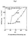
- Figure 1 is a diagram representing the pH dependency of etching rate, of an etching solution according to a first embodiment of the present invention.
- Figure 2 is a diagram showing cross sectional views for explaining an etching method according to the first embodiment of the present invention.
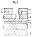
- Figure 3 is a cross sectional view for explaining a recess etching of a HEMT according to the first embodiment of the present invention.
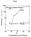
- Figure 4 is a diagram representing the pH dependency of etching rate, of an etching solution according to a second embodiment of the present invention.
- Figure 5 shows cross sectional views for explaining an etching method according to the second embodiment of the present invention.
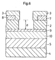
- Figure 6 is a cross sectional view for explaining a recess etching of a HEMT according to the second embodiment of the present invention.
- Figure 7 is a diagram representing the pH dependency of etching rate, of an etching solution according to a third embodiment of the present invention.
- Figure 8 is a diagram showing cross sectional views explaining an etching method according to the third embodiment of the present invention.
- Figure 9 is a cross sectional view for explaining a surface exposing etching of an HBT according to the third embodiment of the present invention.
- Figure 10 is a diagram for explaining the external base resistance at the surface exposing etching of the HBT according to the third embodiment of the present invention.
- Figure 11 is a diagram representing the pH dependency of etching rate, of an etching solution according to a fourth embodiment of the present invention.
- Figure 12 is a diagram showing cross sectional views for explaining the etching method according to the fourth embodiment of the present invention.
- Figure 13 is a diagram showing cross sectional views for explaining an HBT including an emitter layer that is depleted according to the fourth embodiment of the present invention.
- Figure 14 is a diagram representing the pH dependency of etching rate, of an etching solution according to a fifth embodiment of the present invention.
- Figure 15 is a diagram showing cross sectional views explaining an etching method according to the fifth embodiment of the present invention.
- Figure 16 is a cross sectional view for explaining the etching of the emitter layer of the HBT according to the fifth embodiment of the present invention.
- Figure 17 is a cross sectional view for explaining the prior art etching method.
- Figure 18 is a cross sectional view for explaining the recess etching of the prior art HEMT.
- Figure 1 is a diagram for explaining an etching solution according to a first embodiment of the present invention.
- This figure shows the pH dependency of etching rate against GaAs and AlGaAs, of an etching solution obtained from citric acid as organic acid and hydrogen peroxide mixed in a volume ratio of 100:1.
- organic acid generally known organic acid, for example, malic acid, malonic acid, oxalic acid, tartaric acid, and succinic acid may be employed in the present invention.
- the volume ratio of the organic acid and the hydrogen peroxide may be within a range from 1:1 to 200:1, and then it represents the pH dependency of etching rate for GaAs and AlGaAs similar to that shown in figure 1.
- Figure 2(a) and (b) show an etching method according to a first embodiment of the present invention.
- reference numeral 1 designates an n type AlGaAs layer
- reference numeral 2 designates an n+ type GaAs layer
- reference numeral 3 designates photoresist.
- Figure 3 is a diagram for explaining a recess etching of an HEMT employing an etching solution according to a first embodiment of the present invention.
- reference numeral 1 designates an n type AlGaAs electron supply layer
- reference numeral 2 designates an n+ type GaAs cap layer (ohmic contact layer)
- reference numeral 3 designates photoresist
- reference numeral 4 designates a GaAs substrate
- reference numeral 5 designates an i type GaAs buffer layer
- reference numeral 6 designates an i type InGaAs channel layer
- reference numeral 7 designates a drain electrode
- reference numeral 8 designates a source electrode.
- Impurity concentration and thickness of respective layers of the HEMT are shown in the following table 1.
- the etching depth (d) of the n+ type GaAs layer 2 can be controlled at high preciseness, the problem of occurring variation in the threshold voltage V th in the prior art etching method is solved, thereby the characteristics of the HEMT is made uniform.
- Japanese Published Patent Application No.63-62235 discloses a method of performing an etching to a GaAs layer selectively with an AlGaAs mixture crystalline layer using a solution comprising ammonia and hydrogen peroxide in a volume ratio of 1:750 to 1:1500.
- a mixture solution of ammonia and hydrogen peroxide that has not adjusted its pH is employed, an eminent difference in the etching rate as in this first embodiment is not obtained.
- the etching solution is obtained by mixing organic acid and hydrogen peroxide in a volume ratio of 1:1 to 200:1 and basic material is added thereto to produce a pH of 6.0 to 8.0
- an eminent difference in the etching rate is resulted between the GaAs layer and the AlGaAs layer, thereby resulting an easy and high preciseness selective etching.
- FIG 4 is a diagram for explaining an etching solution according to a second embodiment of the present invention.
- citric acid is employed as organic acid, and the citric acid and the hydrogen peroxide are mixed in a volume ratio of 100:1.
- the pH dependency of the etching rates for GaAs and InGaAs are shown in the figure 4.
- citric acid is employed similar to the first embodiment, generally known organic acid as those raised in the first embodiment can be employed.
- the volume ratio of the citric acid and the hydrogen peroxide may be in a range of 1:1 to 200:1, and then the pH dependency of etching rate against GaAs and InGaAs similar to that of figure 4 are obtained.
- Figure 5 is a diagram showing an etching method according to a second embodiment of the present invention, where reference numeral 2 designates an n+ type GaAs layer, reference numeral 9 designates an n type InGaAs layer, and reference numeral 3 designates photoresist.
- Figure 6 is a diagram explaining a recess etching of a MESFET employing an n type InGaAs as a stopper layer 9 employing the etching solution according to the second embodiment, where reference numeral 3 designates photoresist, reference numeral 7 designates a drain electrode, and reference numeral 8 designates a source electrode.
- the threshold voltage V th of this MESFET will be represented as follows:
- the citric acid and the hydrogen peroxide are mixed in a volume ratio of 100:1, and the pH is adjusted to be in a range of pH above 6.0 by adding, for example, basic compound such as ammonia thereto, the selective etching between GaAs and InGaAs is made possible.
- the etching rate of GaAs is large and the etching rate of InGaAs is small, thereby the GaAs is etched a lot and InGaAs is hardly etched.
- This etching can be applied to a case where a recess etching of a MESFET is performed using the InGaAs layer as a stopper layer 9 as shown in figure 6. Then, the etching depth (d) can be controlled at high preciseness, thereby the active layer thickness (a) (the thickness of layers of InGaAs stopper layer 9 and n type GaAs layer 10 in figure 6) becomes uniform, thereby solving the problem of arising variations in the threshold voltage V th due to the variations in the active layer thickness (a) in the formula (2) representing the threshold voltage V th of the MESFET.
- the etching solution is adjusted to have a pH value of above 6.0 by adding basic compound to the mixture solution of organic acid and hydrogen peroxide mixed in a volume ratio of 1:1 to 200:1, an AlAs layer is not required to be formed between the GaAs layer and the InGaAs layer, thereby enabling a selective etching easily and at high preciseness.
- Figure 7 is a diagram for explaining an etching solution according to a third embodiment of the present invention, and shows the pH dependency of etching rate against AlGaAs and InGaAs, of a solution which is a mixture solution of citric acid and hydrogen peroxide mixed in a volume ratio of 100:1.
- a solution which is a mixture solution of citric acid and hydrogen peroxide mixed in a volume ratio of 100:1.
- citric acid is employed.
- the etching solution of organic acid and hydrogen peroxide mixed in a volume ratio within a range of 1:1 to 200:1 shows the pH dependency of the etching rate against AlGaAs and InGaAs similar to that shown in figure 7.
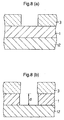
- Figure 8 is a diagram showing an etching method according to the third embodiment of the present invention.
- Reference numeral 1 designates an n type AlGaAs layer
- reference numeral 12 designates a p type InGaAs layer
- reference numeral 3 designates photoresist.
- Figure 9 is a diagram for explaining the base surface exposing etching of an HBT, where reference numeral 11 designates an emitter electrode and reference numeral 3 designates photoresist.
- the impurity concentration and the thicknesses of the respective layers of this HBT are as in the following table 3.
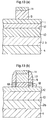
- Figure 10 is a diagram for explaining that the external base resistance increases when the base surface exposing etching is performed in the conventional technique, where reference numeral 11 designates an emitter electrode, reference numeral 13 designates a base layer, reference numeral 14 designates an emitter layer, and reference numeral 15 designates a base electrode.
- the base resistance R B in the HBT is represented by the following formula (3), where Z E is an emitter length.
- the external base resistance in the second term in the formula (3) increases due to that the base layer 13 is overetched, and thereby the X B2 increases, whereby the device characteristic such as the maximum oscillation frequency is deteriorated.
- the etching can be stopped at the upper surface of the base layer 13 of the HBT, whereby the increase of the external base resistance is prevented.
- Figure 11 is a diagram for explaining an etching solution according to a fourth embodiment of the present invention, and the pH dependency of the etching rate for InGaAs and AlGaAs, of a solution employing citric acid as organic acid, and the citric acid and the hydrogen peroxide is mixed in a volume ratio of 40:1.
- a generally known organic acid may be employed as organic acid.
- the volume ratio of the organic acid and the hydrogen peroxide may be in a range of 1:1 to 200:1, presenting the similar pH dependency of the etching rate against AlGaAs and InGaAs as that shown in figure 11.
- Figure 12 is a diagram for explaining an etching solution according to a fourth embodiment of the present invention, where reference numeral 1 designates an n type AlGaAs layer, reference numeral 9 designates an InGaAs layer, and reference numeral 3 designates photoresist.
- Figure 13(a) and 13(b) are diagrams for explaining a method for producing an emitter layer that is depleted, of an HBT.
- reference numeral 11 designates an emitter electrode
- reference numeral 17 designates an SiO2 side wall
- reference numeral 18 designates an AlGaAs emitter layer that is depleted.
- the impurity concentration, and the thickness of the layers of the HBT are shown in the following table 4.
- Table 4 layer impurity concentration thickness type GaAs substrate 4 n+ type GaAs collector contact layer 2b 2 x 1018cm ⁇ 3 2,000 ⁇ n ⁇ type GaAs collector layer 10 1 x 1017cm ⁇ 3 2,000 ⁇ p+ type InGaAs base layer 12 1 x 1019cm ⁇ 3 500 ⁇ n type AlGaAs emitter layer 1 5 x 1017cm ⁇ 3 500 ⁇ InGaAs emitter layer 9 2 x 1018cm ⁇ 3 1,000 ⁇
- the volume ratio of the citric acid and the hydrogen peroxide is 40:1, and basic compound such as ammonia is added thereto to adjust the pH to be 4.5 to 5.5, a selective etching between InGaAs and AlGaAs is enabled.
- an etching is performed to the AlGaAs emitter layer 1 employing the etching solution according to the third embodiment as shown in figure 13(b), and an AlGaAs layer 18 that is depleted is produced.
- a high selectivity etching of InGaAs/AlGaAs is performed using the above-described etching solution, thereby the production of an AlGaAs emitter layer 18 of an HBT that is depleted can be produced easily and at high preciseness.
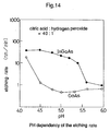
- Figure 14 is a diagram for explaining an etching solution according to a fifth embodiment of the present invention.
- Figure 14 shows the pH dependency of the etching rate for InGaAs and GaAs, of the etching solution which is obtained by that citric acid is employed as organic acid, the citric acid and the hydrogen peroxide are mixed in a volume ratio of 40:1.
- citric acid is employed in this fifth embodiment, generally known organic acid can be employed as organic acid.
- the volume ratio of the organic acid and the hydrogen peroxide may be in a range of 1:1 to 200:1, thereby presenting the pH dependency of the etching rate against AlGaAs and InGaAs similar to that shown in figure 14.
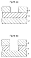
- Figure 15 shows an etching method according to a fifth embodiment of the present invention.
- reference numeral 2 designates an n+ type GaAs layer
- reference numeral 9 designates an InGaAs layer
- reference numeral 3 designates photoresist.
- Figure 16 is a diagram for explaining the etching of an emitter layer of an HBT, where reference numeral 11 designates an emitter electrode.
- Table 5 layer impurity concentration thickness GaAs substrate 4 n+ type GaAs collector contact layer 2b 2 x 1018cm ⁇ 3 2,000 ⁇ n ⁇ type GaAs collector layer 10 1 x 1017cm ⁇ 3 2,000 ⁇ p+ type InGaAs base layer 12 1 x 1019cm ⁇ 3 500 ⁇ n type AlGaAs emitter layer 1 5 x 1017cm ⁇ 3 500 ⁇ n type GaAs emitter layer 10a 2 x 1018cm ⁇ 3 1,000 ⁇ InGaAs emitter layer 9 2 x 1018cm ⁇ 3 1,000 ⁇
- a high selectivity etching of InGaAs/GaAs can be performed using the above-described etching solution, thereby a heterostructure device such as HBT can be produced.
- an etching solution presenting an eminent difference in the etching rate between GaAs/AlGaAs, GaAs/InGaAs, AlGaAs/InGaAs, InGaAs/AlGaAs, and InGaAs/GaAs is obtained, enabling a high selectivity etching easily and at high preciseness. Thereby, a precise control of an etching for a heterostructure semiconductor is enabled.
Landscapes
- Weting (AREA)
- Bipolar Transistors (AREA)
- Junction Field-Effect Transistors (AREA)
Applications Claiming Priority (2)
| Application Number | Priority Date | Filing Date | Title |
|---|---|---|---|
| JP59758/93 | 1993-03-19 | ||
| JP5975893 | 1993-03-19 |
Publications (2)
| Publication Number | Publication Date |
|---|---|
| EP0617458A2 true EP0617458A2 (de) | 1994-09-28 |
| EP0617458A3 EP0617458A3 (de) | 1994-12-21 |
Family
ID=13122488
Family Applications (1)
| Application Number | Title | Priority Date | Filing Date |
|---|---|---|---|
| EP93120476A Ceased EP0617458A3 (de) | 1993-03-19 | 1993-12-17 | Verfahren zum Ätzen von Halbleitern und Ätzlösung dafür. |
Country Status (2)
| Country | Link |
|---|---|
| US (1) | US5419808A (de) |
| EP (1) | EP0617458A3 (de) |
Cited By (4)
| Publication number | Priority date | Publication date | Assignee | Title |
|---|---|---|---|---|
| FR2722511A1 (fr) * | 1994-07-15 | 1996-01-19 | Ontrak Systems Inc | Procede pour enlever les metaux dans un dispositif de recurage |
| EP0642425A4 (de) * | 1993-03-25 | 1996-11-06 | Watkins Johnson Co | Verfahren zur herstellung iii-iv verbindung halbleiter bauelemente mit selektiver ätzung. |
| WO1997024754A1 (en) * | 1995-12-29 | 1997-07-10 | Philips Electronics N.V. | Preferential etch of semiconductor substrate with respect to epitaxial layers |
| EP1737026A1 (de) * | 2005-06-22 | 2006-12-27 | Sumitomo Electric Industries, Ltd. | Verfahren zur Oberflächenbehandlung von III-V-Halbleitersubstraten und Verfahren zur Herstellung von III-V-Verbindungshalbleitern |
Families Citing this family (7)
| Publication number | Priority date | Publication date | Assignee | Title |
|---|---|---|---|---|
| JP3640272B2 (ja) * | 1996-02-09 | 2005-04-20 | 三菱電機株式会社 | 半導体装置の製造方法 |
| JP3097557B2 (ja) * | 1996-05-20 | 2000-10-10 | 日本電気株式会社 | 半導体装置の製造方法 |
| US5895941A (en) * | 1996-07-01 | 1999-04-20 | Mitsubishi Denki Kabushiki Kaisha | Field effect transistor with electrode portions under T-shaped gate structure |
| US6436300B2 (en) | 1998-07-30 | 2002-08-20 | Motorola, Inc. | Method of manufacturing electronic components |
| JP2001007118A (ja) * | 1999-06-22 | 2001-01-12 | Nec Corp | 半導体装置及びその製造方法 |
| US6737288B2 (en) * | 2001-05-24 | 2004-05-18 | Mitsubishi Denki Kabushiki Kaisha | Method for fabricating a semiconductor device |
| JP3858888B2 (ja) * | 2003-12-02 | 2006-12-20 | ソニー株式会社 | エッチング方法及び半導体装置の製造方法 |
Family Cites Families (7)
| Publication number | Priority date | Publication date | Assignee | Title |
|---|---|---|---|---|
| JPS6029518A (ja) * | 1983-07-27 | 1985-02-14 | Hitachi Ltd | グロ−プラグ用ヒ−タ |
| JPS6362235A (ja) * | 1986-09-02 | 1988-03-18 | Fuji Electric Co Ltd | 半導体の蝕刻方法 |
| NL8701184A (nl) * | 1987-05-18 | 1988-12-16 | Philips Nv | Werkwijze voor het vervaardigen van een halfgeleiderinrichting. |
| JPH02206117A (ja) * | 1989-02-06 | 1990-08-15 | Yokogawa Electric Corp | 半導体装置の製造方法 |
| US5110765A (en) * | 1990-11-30 | 1992-05-05 | At&T Bell Laboratories | Selective etch for GaAs-containing group III-V compounds |
| JPH04261082A (ja) * | 1991-02-06 | 1992-09-17 | Mitsubishi Electric Corp | 半導体レ−ザ装置 |
| JP3082401B2 (ja) * | 1992-03-25 | 2000-08-28 | 松下電器産業株式会社 | 選択エッチング液および半導体装置の製造方法 |
-
1993
- 1993-11-22 US US08/155,325 patent/US5419808A/en not_active Expired - Lifetime
- 1993-12-17 EP EP93120476A patent/EP0617458A3/de not_active Ceased
Cited By (7)
| Publication number | Priority date | Publication date | Assignee | Title |
|---|---|---|---|---|
| EP0642425A4 (de) * | 1993-03-25 | 1996-11-06 | Watkins Johnson Co | Verfahren zur herstellung iii-iv verbindung halbleiter bauelemente mit selektiver ätzung. |
| USRE36185E (en) * | 1993-03-25 | 1999-04-06 | Watkins Johnson Company | Method of fabricating Group III-V compound semiconductor devices using selective etching |
| FR2722511A1 (fr) * | 1994-07-15 | 1996-01-19 | Ontrak Systems Inc | Procede pour enlever les metaux dans un dispositif de recurage |
| WO1997024754A1 (en) * | 1995-12-29 | 1997-07-10 | Philips Electronics N.V. | Preferential etch of semiconductor substrate with respect to epitaxial layers |
| US5756403A (en) * | 1995-12-29 | 1998-05-26 | Philips Electronics North America | Method of preferentially etching a semiconductor substrate with respect to epitaxial layers |
| EP1737026A1 (de) * | 2005-06-22 | 2006-12-27 | Sumitomo Electric Industries, Ltd. | Verfahren zur Oberflächenbehandlung von III-V-Halbleitersubstraten und Verfahren zur Herstellung von III-V-Verbindungshalbleitern |
| US7432186B2 (en) | 2005-06-22 | 2008-10-07 | Sumitomo Electric Industries, Ltd | Method of surface treating substrates and method of manufacturing III-V compound semiconductors |
Also Published As
| Publication number | Publication date |
|---|---|
| US5419808A (en) | 1995-05-30 |
| EP0617458A3 (de) | 1994-12-21 |
Similar Documents
| Publication | Publication Date | Title |
|---|---|---|
| US5468343A (en) | Etching solution and etching method for semiconductors and method for evaluating GaAs surface | |
| EP0551110B1 (de) | Verbindungshalbleiterbauelemente | |
| US6573129B2 (en) | Gate electrode formation in double-recessed transistor by two-step etching | |
| US4733283A (en) | GaAs semiconductor device | |
| US6797994B1 (en) | Double recessed transistor | |
| US5284782A (en) | Process for formation of delta-doped quantum well field effect transistor | |
| US4984036A (en) | Field effect transistor with multiple grooves | |
| DE69324630T2 (de) | Dotierungsverfahren, Halbleiterbauelement und Verfahren zu seiner Herstellung | |
| EP0617458A2 (de) | Verfahren zum Ätzen von Halbleitern und Ätzlösung dafür | |
| EP1131849B1 (de) | Pseudomorphe transistoren mit hoher elektronenbeweglichkeit | |
| US5486710A (en) | Field effect transistor | |
| US5334865A (en) | MODFET structure for threshold control | |
| US6656802B2 (en) | Process of manufacturing a semiconductor device including a buried channel field effect transistor | |
| DE4400233C2 (de) | Feldeffekttransistor | |
| KR19990013312A (ko) | 반도체장치의 제조방법 | |
| US5532505A (en) | Field effect transistor including a cap with a doped layer formed therein | |
| US5389807A (en) | Field effect transistor | |
| JPH04125940A (ja) | 電界効果トランジスタ及びその製造方法 | |
| JP3653652B2 (ja) | 半導体装置 | |
| JP3381694B2 (ja) | 半導体装置及びその製造方法 | |
| JP3112075B2 (ja) | 電界効果トランジスタ及びその製造方法 | |
| JPH04280640A (ja) | 電界効果トランジスタ及びその製造方法 | |
| JP3109097B2 (ja) | 電界効果トランジスタの製造方法およびエッチング方法 | |
| JPH0797634B2 (ja) | 電界効果トランジスタとその製造方法 | |
| Xu et al. | Electrochemically induced asymmetrical etching in InAlAs/InGaAs heterostructures for MODFET gate-groove fabrication |
Legal Events
| Date | Code | Title | Description |
|---|---|---|---|
| PUAI | Public reference made under article 153(3) epc to a published international application that has entered the european phase |
Free format text: ORIGINAL CODE: 0009012 |
|
| AK | Designated contracting states |
Kind code of ref document: A2 Designated state(s): DE FR GB |
|
| PUAL | Search report despatched |
Free format text: ORIGINAL CODE: 0009013 |
|
| AK | Designated contracting states |
Kind code of ref document: A3 Designated state(s): DE FR GB |
|
| 17P | Request for examination filed |
Effective date: 19941216 |
|
| 17Q | First examination report despatched |
Effective date: 19960923 |
|
| STAA | Information on the status of an ep patent application or granted ep patent |
Free format text: STATUS: THE APPLICATION HAS BEEN REFUSED |
|
| 18R | Application refused |
Effective date: 19990410 |