EP0585090A2 - Phasenregelkreissystem mit Kompensierung der Änderungen der datenflankenabhängigen Schleifenverstärkung - Google Patents
Phasenregelkreissystem mit Kompensierung der Änderungen der datenflankenabhängigen Schleifenverstärkung Download PDFInfo
- Publication number
- EP0585090A2 EP0585090A2 EP93306642A EP93306642A EP0585090A2 EP 0585090 A2 EP0585090 A2 EP 0585090A2 EP 93306642 A EP93306642 A EP 93306642A EP 93306642 A EP93306642 A EP 93306642A EP 0585090 A2 EP0585090 A2 EP 0585090A2
- Authority
- EP
- European Patent Office
- Prior art keywords
- signal
- clock signal
- loop
- phase
- gain
- Prior art date
- Legal status (The legal status is an assumption and is not a legal conclusion. Google has not performed a legal analysis and makes no representation as to the accuracy of the status listed.)
- Granted
Links
Images

Classifications
-
- H—ELECTRICITY
- H03—ELECTRONIC CIRCUITRY
- H03L—AUTOMATIC CONTROL, STARTING, SYNCHRONISATION OR STABILISATION OF GENERATORS OF ELECTRONIC OSCILLATIONS OR PULSES
- H03L7/00—Automatic control of frequency or phase; Synchronisation
- H03L7/06—Automatic control of frequency or phase; Synchronisation using a reference signal applied to a frequency- or phase-locked loop
- H03L7/08—Details of the phase-locked loop
- H03L7/085—Details of the phase-locked loop concerning mainly the frequency- or phase-detection arrangement including the filtering or amplification of its output signal
- H03L7/089—Details of the phase-locked loop concerning mainly the frequency- or phase-detection arrangement including the filtering or amplification of its output signal the phase or frequency detector generating up-down pulses
- H03L7/0891—Details of the phase-locked loop concerning mainly the frequency- or phase-detection arrangement including the filtering or amplification of its output signal the phase or frequency detector generating up-down pulses the up-down pulses controlling source and sink current generators, e.g. a charge pump
- H03L7/0895—Details of the current generators
- H03L7/0898—Details of the current generators the source or sink current values being variable
-
- H—ELECTRICITY
- H03—ELECTRONIC CIRCUITRY
- H03L—AUTOMATIC CONTROL, STARTING, SYNCHRONISATION OR STABILISATION OF GENERATORS OF ELECTRONIC OSCILLATIONS OR PULSES
- H03L7/00—Automatic control of frequency or phase; Synchronisation
- H03L7/06—Automatic control of frequency or phase; Synchronisation using a reference signal applied to a frequency- or phase-locked loop
- H03L7/08—Details of the phase-locked loop
- H03L7/10—Details of the phase-locked loop for assuring initial synchronisation or for broadening the capture range
-
- H—ELECTRICITY
- H03—ELECTRONIC CIRCUITRY
- H03L—AUTOMATIC CONTROL, STARTING, SYNCHRONISATION OR STABILISATION OF GENERATORS OF ELECTRONIC OSCILLATIONS OR PULSES
- H03L7/00—Automatic control of frequency or phase; Synchronisation
- H03L7/06—Automatic control of frequency or phase; Synchronisation using a reference signal applied to a frequency- or phase-locked loop
- H03L7/08—Details of the phase-locked loop
- H03L7/10—Details of the phase-locked loop for assuring initial synchronisation or for broadening the capture range
- H03L7/107—Details of the phase-locked loop for assuring initial synchronisation or for broadening the capture range using a variable transfer function for the loop, e.g. low pass filter having a variable bandwidth
-
- H—ELECTRICITY
- H03—ELECTRONIC CIRCUITRY
- H03L—AUTOMATIC CONTROL, STARTING, SYNCHRONISATION OR STABILISATION OF GENERATORS OF ELECTRONIC OSCILLATIONS OR PULSES
- H03L7/00—Automatic control of frequency or phase; Synchronisation
- H03L7/06—Automatic control of frequency or phase; Synchronisation using a reference signal applied to a frequency- or phase-locked loop
- H03L7/08—Details of the phase-locked loop
- H03L7/10—Details of the phase-locked loop for assuring initial synchronisation or for broadening the capture range
- H03L7/107—Details of the phase-locked loop for assuring initial synchronisation or for broadening the capture range using a variable transfer function for the loop, e.g. low pass filter having a variable bandwidth
- H03L7/1072—Details of the phase-locked loop for assuring initial synchronisation or for broadening the capture range using a variable transfer function for the loop, e.g. low pass filter having a variable bandwidth by changing characteristics of the charge pump, e.g. changing the gain
Definitions
- This invention relates to phase locked loop (PLL) systems in which the density of data transitions in the data signal varies.
- Monolithic PLL circuits have become the basic building blocks of many consumer and industrial electronic systems.
- the PLL is an integral part of the clock recovery subsystem.
- the PLL may be used to recover the clock signal from the data signal; the recovered clock may then be used, for example, to regenerate the data signal.
- the basic PLL system generally comprises three elements: (1) a phase detector, (2) a loop filter, and (3) a voltage controlled oscillator (VCO), which are interconnected in a feedback system as shown in FIG. 12.1 of "Bipolar and MOS Analog Integrated Circuit Design," A. B. Grebene, John Wiley & Sons (1984).
- the phase detector compares the phase of an input signal V s with the phase of the VCO and generates a control voltage V d .
- This voltage V d is filtered by the loop filter, the output of which is applied to the control terminal of the VCO to control its frequency of oscillation.
- K L K D K o
- K D (V/rad) is the phase detector conversion gain
- K O (HZ/V) is the voltage-to-frequency conversion gain of the VCO.
- phase detector gain K D and hence the loop gain, of a clock recovery PLL is dependent on the transition density of the data signal.
- the loop gain of a PLL is made to be essentially constant by compensating for the dependence of that gain on the data transition density of an input data signal.
- the loop gain is made to be controllably responsive to the transition density of the input data signal so as to increase the loop gain when the density is relatively low and, conversely, to decrease the gain when the density is relatively high.
- the number of clock transitions (either rising or falling) between adjacent data transitions is counted and used to adjust the loop gain.
- the average loop gain is essentially constant with changes in transition density.
- This method is illustratively implemented in a PLL which includes a modulator for altering the loop gain in response to the difference between the data transition density of the input signal and the clock signal.
- the modulator comprises a charge pump located between the phase detector and the loop filter. The charge pump supplies current pulses to the filter, the amplitude of the pulses being related to the data transition density; the lower the data transition density in a given time interval, the higher the pulse amplitude (and conversely).
- the invention is particularly attractive for use in systems in which there is an upper bound on the number of data bits which can occur without a data transition also occurring.
- Examples of such systems are those employing Manchester coding or Run Length Limited coding schemes.
- the invention in general makes the loop gain of a PLL system controllably responsive to the transition density of a data signal.
- the invention makes the loop gain essentially constant even though the transition density may vary.
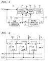
- FIG. 3 A block diagram of a PLL system 10 in accordance with one embodiment of the invention is shown in FIG. 3.
- the system includes a feedback loop 12 formed by a phase detector 14, a loop gain modulator (e.g., a charge pump 16), a loop filter 18, and a voltage controlled oscillator (VCO) 20.
- a data transition comparator 22 Located outside the loop 12, a data transition comparator 22 compares the transitions of the input data signal V s with those of the clock V o (i.e., the VCO output) and generates pulse width modulated (PWM) control pulses V T .
- the PWM pulses V T control the magnitude of pulse amplitude modulated (PAM) current pulses I c supplied by charge pump 16 to loop filter 18.
- PAM pulse amplitude modulated
- V c which controls the frequency of VCO 20.
- Loop filter 18, which may be active or passive, VCO 20, which may be a relaxation oscillator, and transition comparator 22, which may simply be a differentiator followed by rectifier, are all well-known in the art.
- Phase detector 14 may be any one of a class of well known detectors suitable for handling non-periodic data signals. As shown in FIG. 3, phase detector 14 has two inputs: the input data signal V s and the output signal (clock) V o of VCO 20. Detector 14 compares the phases of V s and V o and generates two outputs, V d and V u , but three allowable states. That is, these outputs are logic levels applied to the charge pump 16: (1) V u alone is true when the output frequency of VCO 20 needs to be increased, (2) V d alone is true when the output frequency of VCO 20 needs to be decreased, and (3) V u and V d are false simultaneously when the output frequency of VCO 20 is to remain unchanged.
- the PLL dynamically adjusts the current pulse amplitudes so that the phase detector gain, and hence the loop gain, compensates for variations in density. Effectively, therefore, the gain and hence the loop dynamics are maintained essentially constant over a relatively wide range of data transition densities.
- the effective phase detector gain (and hence the loop gain) is dynamically adjusted by means of charge pump 16 and comparator 22.
- the sign of the pulse may be either positive or negative depending on whether the clock signal is lagging or leading the data signal, respectively.
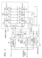
- the loop filter 18 is a standard second-order filter having the series combination of a resistor R1 and a capacitor C1 connected between its input terminal and ground, with smoothing capacitor C2 connected in parallel with the R1-C1 combination.
- the data transition comparator 22 comprises a data transition detector 22.1 (e.g., a differentiator followed by a rectifier) with its input coupled to V s and its output coupled to the clear input CLR of counter 22.2.
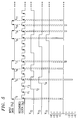
- the width of the current pulses I c is related to the phase error generated by the phase detector and as a result may vary considerably (e.g., 0-50%). In the interest of simplicity, however, FIG. 5 shows the pulses I c to be of equal duration.
- the phase detector 14 compares the rising edge (for example) of the clock signal V o to a data transition of input signal V s . Assuming a positive VCO gain K o and an "early" clock transition, then a pulse would be generated on the "down" output V d . This pulse would cause the control voltage V c to decrease, thus slowing the frequency of V o (i.e., the clock rate). Note, however, the clock in FIG. 5 is shown to have a constant frequency in the interests of simplicity (i.e., in many cases the actual frequency shift would be imperceptible in a schematic drawing). Conversely, if the clock transition were "late”, a pulse would be generated on the "up" output V u to accelerate the clock rate.
- FIG. 5 shows, for example, additional control current pulses of amplitude +2I, -I, +4I, -I, -I, and +I, respectively, being generated by the charge pump at times t6 to t11, respectively.
- the phase detector gain and hence the loop gain, is adjusted to compensate for the changing transition density of the data signal.
- the invention is advantageously used in systems where the data is coded so that there is an upper bound on the number of data bits which can occur between data transitions.
- Examples of such coding schemes are Manchester coding and Run Length Limited coding.
- the invention is not limited to such use in such systems.
- the PLL would still provide loop gain compensation, and hence be an improvement over the prior art, up to the point where the charge pump had already switched in the maximum number of current sources provided by the physical design even though a relatively low transition density data signal may be "demanding" more current.
Landscapes
- Stabilization Of Oscillater, Synchronisation, Frequency Synthesizers (AREA)
- Synchronisation In Digital Transmission Systems (AREA)
Applications Claiming Priority (2)
| Application Number | Priority Date | Filing Date | Title |
|---|---|---|---|
| US936824 | 1992-08-28 | ||
| US07/936,824 US5315270A (en) | 1992-08-28 | 1992-08-28 | Phase-locked loop system with compensation for data-transition-dependent variations in loop gain |
Publications (3)
| Publication Number | Publication Date |
|---|---|
| EP0585090A2 true EP0585090A2 (de) | 1994-03-02 |
| EP0585090A3 EP0585090A3 (de) | 1995-01-04 |
| EP0585090B1 EP0585090B1 (de) | 1999-07-21 |
Family
ID=25469122
Family Applications (1)
| Application Number | Title | Priority Date | Filing Date |
|---|---|---|---|
| EP93306642A Expired - Lifetime EP0585090B1 (de) | 1992-08-28 | 1993-08-20 | Phasenregelkreissystem mit Kompensierung der Änderungen der datenflankenabhängigen Schleifenverstärkung |
Country Status (5)
| Country | Link |
|---|---|
| US (1) | US5315270A (de) |
| EP (1) | EP0585090B1 (de) |
| JP (1) | JPH06188727A (de) |
| KR (1) | KR940004972A (de) |
| DE (1) | DE69325685T2 (de) |
Cited By (12)
| Publication number | Priority date | Publication date | Assignee | Title |
|---|---|---|---|---|
| EP0692879A1 (de) * | 1994-07-12 | 1996-01-17 | General Instrument Corporation Of Delaware | Ringoszillator mit einer Frequenzregelschleife |
| WO2000002317A1 (en) * | 1998-07-01 | 2000-01-13 | Conexant Systems, Inc. | Method and apparatus for adjusting phase offset in a phase locked loop |
| WO2000060806A3 (en) * | 1999-04-02 | 2001-01-25 | Storage Technology Corp | Dropout resistant phase-locked loop |
| EP1225698A1 (de) * | 2001-01-22 | 2002-07-24 | Lucent Technologies Inc. | Verfahren und Anordnung zur Korrektur der Taktphase in einem Datenempfänger mit einem Hogge oder Alexander Phasendiskriminator |
| EP1434350A1 (de) * | 2002-12-23 | 2004-06-30 | Agilent Technologies, Inc. | System und Verfahren zur Beseitigung des Verstärkungsfehlers eines Phasendetektors bei der Taktrückgewinnung verursacht durch datanabhängig variierende Anzahl von Flankenwechseln |
| EP1473834A1 (de) * | 2003-04-30 | 2004-11-03 | STMicroelectronics S.r.l. | Verfahren und Schaltung zum Messen der Transitionsdichte eines Signals und Verfahren und Anordnung zur Phasendetektion mit variabler Verstärkung |
| WO2004095769A3 (en) * | 2003-03-31 | 2004-12-16 | Intel Corp | Local receive clock signal adjustment |
| KR100490637B1 (ko) * | 1997-12-29 | 2005-10-21 | 삼성전자주식회사 | 기억장치를이용한고속zclv위상동기장치 |
| WO2005101665A1 (en) * | 2004-04-15 | 2005-10-27 | Koninklijke Philips Electronics N.V. | Phase locked loop circuit |
| US7075866B2 (en) | 2000-11-16 | 2006-07-11 | Matsushita Electric Industrial Co., Ltd. | Clock extracting device of a disc reproducing apparatus having a gain command unit for designating a loop gain |
| CN106301360A (zh) * | 2015-05-28 | 2017-01-04 | 上海东软载波微电子有限公司 | 鉴频鉴相器、电荷泵和锁相环电路 |
| CN107911113A (zh) * | 2017-10-31 | 2018-04-13 | 北京集创北方科技股份有限公司 | 时钟数据恢复电路及其环路带宽调节方法、处理器 |
Families Citing this family (45)
| Publication number | Priority date | Publication date | Assignee | Title |
|---|---|---|---|---|
| JP3241079B2 (ja) * | 1992-02-24 | 2001-12-25 | 株式会社日立製作所 | ディジタル位相同期回路 |
| JP3643385B2 (ja) * | 1993-05-19 | 2005-04-27 | 株式会社東芝 | 半導体回路装置 |
| US5473639A (en) * | 1993-07-26 | 1995-12-05 | Hewlett-Packard Company | Clock recovery apparatus with means for sensing an out of lock condition |
| US5513225A (en) * | 1994-08-31 | 1996-04-30 | International Business Machines Corporation | Resistorless phase locked loop circuit employing direct current injection |
| US5619161A (en) * | 1994-08-31 | 1997-04-08 | International Business Machines Corporation | Diffrential charge pump with integrated common mode control |
| US5525932A (en) * | 1994-08-31 | 1996-06-11 | International Business Machines Corporation | Lock indicator for phase locked loop circuit |
| US5491439A (en) * | 1994-08-31 | 1996-02-13 | International Business Machines Corporation | Method and apparatus for reducing jitter in a phase locked loop circuit |
| US5495207A (en) * | 1994-08-31 | 1996-02-27 | International Business Machines Corporation | Differential current controlled oscillator with variable load |
| JPH0897711A (ja) * | 1994-09-26 | 1996-04-12 | Nec Eng Ltd | Pll回路 |
| US5594763A (en) * | 1995-06-06 | 1997-01-14 | Cirrus Logic, Inc. | Fast synchronizing digital phase-locked loop for recovering clock information from encoded data |
| US5592129A (en) * | 1995-06-22 | 1997-01-07 | National Semiconductor Corporation | High resolution, large multiplication factor digitally-controlled frequency multiplier |
| US5767746A (en) * | 1996-06-07 | 1998-06-16 | David Sarnoff Research Center, Inc. | Method and apparatus for adjusting phase-lock-loop parameters |
| JP2002513515A (ja) | 1996-06-10 | 2002-05-08 | モーフィックス テクノロジー インコーポレイテッド | 情報通信用の方法及び装置 |
| US5838180A (en) * | 1996-09-12 | 1998-11-17 | Lucent Technologies Inc. | Low-voltage frequency synthesizer |
| JP3784485B2 (ja) * | 1997-02-12 | 2006-06-14 | 富士通株式会社 | 出力パルス幅制御システム |
| CA2201695C (en) * | 1997-04-03 | 2004-08-10 | Gennum Corporation | Phase detector for high speed clock recovery from random binary signals |
| US5864176A (en) * | 1997-04-04 | 1999-01-26 | Unisys Corporation | Electro-mechnical subassembly having a greatly reduced thermal resistance between two mating faces by including a film of liquid, that evaporates without leaving any residue, between the faces |
| KR19990009178A (ko) * | 1997-07-08 | 1999-02-05 | 윤종용 | 데드 존이 없는 디지탈 위상 동기 루프와 위상 비교 및 전하 펌핑 방법 |
| US6178207B1 (en) * | 1998-01-09 | 2001-01-23 | Cubic Defense Systems, Inc. | Aircraft combat training signal processing system |
| US6111712A (en) * | 1998-03-06 | 2000-08-29 | Cirrus Logic, Inc. | Method to improve the jitter of high frequency phase locked loops used in read channels |
| CA2234037A1 (en) | 1998-04-03 | 1999-10-03 | Mohammad Hossein Shakiba | Latch-up recovery in quantized feedback dc restorer circuits |
| WO2001041351A1 (en) * | 1999-12-03 | 2001-06-07 | Fujitsu Limited | Phase synchronization loop circuit and optical repeater provided with the circuit, optical terminal station device and optical communication system |
| US6265947B1 (en) * | 2000-01-11 | 2001-07-24 | Ericsson Inc. | Power conserving phase-locked loop and method |
| US6608875B1 (en) * | 2000-05-02 | 2003-08-19 | Tektronix, Inc. | Free-running-frequency adjustment circuit for a clock recovery system |
| US6810024B1 (en) | 2000-06-21 | 2004-10-26 | Agere Systems Inc. | Auto-detection system and method for a network transceiver |
| US6583675B2 (en) * | 2001-03-20 | 2003-06-24 | Broadcom Corporation | Apparatus and method for phase lock loop gain control using unit current sources |
| US6509801B1 (en) | 2001-06-29 | 2003-01-21 | Sierra Monolithics, Inc. | Multi-gigabit-per-sec clock recovery apparatus and method for optical communications |
| US6981168B2 (en) * | 2002-01-08 | 2005-12-27 | International Business Machines Corporation | Clock data recovery system |
| US6664831B2 (en) * | 2002-04-24 | 2003-12-16 | Sun Microsystems, Inc. | Circuit for post-silicon control of delay locked loop charge pump current |
| US6664828B2 (en) * | 2002-04-24 | 2003-12-16 | Sun Microsystems, Inc. | Post-silicon control of phase locked loop charge pump current |
| US6819164B1 (en) * | 2002-10-17 | 2004-11-16 | National Semiconductor Corporation | Apparatus and method for a precision bi-directional trim scheme |
| US7158601B1 (en) * | 2002-10-28 | 2007-01-02 | Cypress Semiconductor Corporation | Clock data recovery method and circuit for network communication |
| US6941116B2 (en) * | 2002-11-27 | 2005-09-06 | Broadcom Corp. | Linearization technique for phase locked loops employing differential charge pump circuitry |
| US6788155B2 (en) * | 2002-12-31 | 2004-09-07 | Intel Corporation | Low gain phase-locked loop circuit |
| US6956923B1 (en) * | 2003-01-17 | 2005-10-18 | Xilinx, Inc. | High speed phase detector architecture |
| DE102004031913A1 (de) * | 2004-06-21 | 2006-01-05 | Atmel Germany Gmbh | Ladungspumpe einer Phasenregelschleife mit umschaltbarer Systembandbreite und Verfahren zur Steuerung einer solchen Ladungspumpe |
| CA2490396A1 (en) * | 2004-12-16 | 2006-06-16 | Galt Display Rack Co. Ltd. | Carpet display rack |
| US7167037B2 (en) * | 2005-06-07 | 2007-01-23 | Northrop Grumman Corporation | Charge pump bias network |
| CN1956337B (zh) * | 2005-10-24 | 2011-03-30 | 北京六合万通微电子技术股份有限公司 | 锁相环频率综合器中寄生参考频率的消除方法及装置 |
| DE102005054846A1 (de) * | 2005-11-15 | 2007-05-24 | Rwth Aachen | Verfahren und Vorrichtung zur Phasenbestimmung |
| US7769121B2 (en) * | 2005-12-22 | 2010-08-03 | Realtek Semiconductor Corporation | Phase detector for data communications |
| KR100817071B1 (ko) * | 2006-10-30 | 2008-03-26 | 삼성전자주식회사 | 사이드 밴드 신호의 펄스 폭 측정 장치 및 그 방법 |
| JP2009267775A (ja) * | 2008-04-25 | 2009-11-12 | Renesas Technology Corp | Pll回路およびシリアルインターフェース回路 |
| US7956694B1 (en) * | 2008-05-12 | 2011-06-07 | Wilson Jeffrey D | Phase controlled dimmer using a narrow band quadrature demodulator |
| US11621715B1 (en) * | 2022-01-11 | 2023-04-04 | Texas Instruments Incorporated | Coarse equalizer adaptation and rate detection for high-speed retimers |
Family Cites Families (6)
| Publication number | Priority date | Publication date | Assignee | Title |
|---|---|---|---|---|
| US4644420A (en) * | 1984-03-29 | 1987-02-17 | Archive Corporation | Circuit and methodology for reading and tracking binary data from magnetic tape independently of the data pattern on the tape |
| US4876518A (en) * | 1988-12-02 | 1989-10-24 | Motorola Inc. | Frequency tracking system |
| US4926141A (en) * | 1989-05-01 | 1990-05-15 | Motorola, Inc. | Frequency synthesizer with improved automatic control of loop bandwidth selection |
| SE8903799D0 (sv) * | 1989-11-13 | 1989-11-13 | Ericsson Telefon Ab L M | Foerfarande och anordning foer att variera slingbandbredden hos en faslaast slinga |
| DE4017491C2 (de) * | 1990-05-31 | 2002-05-08 | Siemens Ag | Abstimmschaltung |
| US5173664A (en) * | 1991-09-16 | 1992-12-22 | Minnesota Mining And Manufacturing Company | Phase locked loop having constant gain for recovering clock from non-uniformly spaced data |
-
1992
- 1992-08-28 US US07/936,824 patent/US5315270A/en not_active Expired - Lifetime
-
1993
- 1993-08-16 JP JP5222305A patent/JPH06188727A/ja active Pending
- 1993-08-17 KR KR1019930015875A patent/KR940004972A/ko not_active Abandoned
- 1993-08-20 DE DE69325685T patent/DE69325685T2/de not_active Expired - Fee Related
- 1993-08-20 EP EP93306642A patent/EP0585090B1/de not_active Expired - Lifetime
Cited By (19)
| Publication number | Priority date | Publication date | Assignee | Title |
|---|---|---|---|---|
| EP0692879A1 (de) * | 1994-07-12 | 1996-01-17 | General Instrument Corporation Of Delaware | Ringoszillator mit einer Frequenzregelschleife |
| KR100490637B1 (ko) * | 1997-12-29 | 2005-10-21 | 삼성전자주식회사 | 기억장치를이용한고속zclv위상동기장치 |
| WO2000002317A1 (en) * | 1998-07-01 | 2000-01-13 | Conexant Systems, Inc. | Method and apparatus for adjusting phase offset in a phase locked loop |
| WO2000060806A3 (en) * | 1999-04-02 | 2001-01-25 | Storage Technology Corp | Dropout resistant phase-locked loop |
| US6775344B1 (en) | 1999-04-02 | 2004-08-10 | Storage Technology Corporation | Dropout resistant phase-locked loop |
| US7075866B2 (en) | 2000-11-16 | 2006-07-11 | Matsushita Electric Industrial Co., Ltd. | Clock extracting device of a disc reproducing apparatus having a gain command unit for designating a loop gain |
| EP1225698A1 (de) * | 2001-01-22 | 2002-07-24 | Lucent Technologies Inc. | Verfahren und Anordnung zur Korrektur der Taktphase in einem Datenempfänger mit einem Hogge oder Alexander Phasendiskriminator |
| US7065160B2 (en) | 2001-01-22 | 2006-06-20 | Lucent Technologies Inc. | Method and apparatus for correcting the phase of a clock in a data receiver |
| EP1434350A1 (de) * | 2002-12-23 | 2004-06-30 | Agilent Technologies, Inc. | System und Verfahren zur Beseitigung des Verstärkungsfehlers eines Phasendetektors bei der Taktrückgewinnung verursacht durch datanabhängig variierende Anzahl von Flankenwechseln |
| US7173995B2 (en) | 2002-12-23 | 2007-02-06 | Avago Technologies General Ip (Singapore) Pte. Ltd. | Systems and methods for correcting gain error due to transition density variation in clock recovery systems |
| CN100421355C (zh) * | 2002-12-23 | 2008-09-24 | 安捷伦科技有限公司 | 用于校正由跳变密度变化引起的增益误差的系统和方法 |
| WO2004095769A3 (en) * | 2003-03-31 | 2004-12-16 | Intel Corp | Local receive clock signal adjustment |
| US7478257B2 (en) | 2003-03-31 | 2009-01-13 | Intel Corporation | Local receive clock signal adjustment |
| EP1473834A1 (de) * | 2003-04-30 | 2004-11-03 | STMicroelectronics S.r.l. | Verfahren und Schaltung zum Messen der Transitionsdichte eines Signals und Verfahren und Anordnung zur Phasendetektion mit variabler Verstärkung |
| WO2005101665A1 (en) * | 2004-04-15 | 2005-10-27 | Koninklijke Philips Electronics N.V. | Phase locked loop circuit |
| CN106301360A (zh) * | 2015-05-28 | 2017-01-04 | 上海东软载波微电子有限公司 | 鉴频鉴相器、电荷泵和锁相环电路 |
| CN106301360B (zh) * | 2015-05-28 | 2019-05-03 | 上海东软载波微电子有限公司 | 鉴频鉴相器、电荷泵和锁相环电路 |
| CN107911113A (zh) * | 2017-10-31 | 2018-04-13 | 北京集创北方科技股份有限公司 | 时钟数据恢复电路及其环路带宽调节方法、处理器 |
| CN107911113B (zh) * | 2017-10-31 | 2021-01-12 | 北京集创北方科技股份有限公司 | 时钟数据恢复电路及其环路带宽调节方法、处理器 |
Also Published As
| Publication number | Publication date |
|---|---|
| KR940004972A (ko) | 1994-03-16 |
| DE69325685T2 (de) | 2000-06-29 |
| EP0585090A3 (de) | 1995-01-04 |
| DE69325685D1 (de) | 1999-08-26 |
| US5315270A (en) | 1994-05-24 |
| EP0585090B1 (de) | 1999-07-21 |
| JPH06188727A (ja) | 1994-07-08 |
Similar Documents
| Publication | Publication Date | Title |
|---|---|---|
| US5315270A (en) | Phase-locked loop system with compensation for data-transition-dependent variations in loop gain | |
| EP0244122B1 (de) | Digitale, phasenverriegelte Taktwiedergewinnungsschleife | |
| CA1284361C (en) | Analog phase locked loop | |
| KR970003097B1 (ko) | 다단 제어구조를 갖는 고속 비트동기 장치 | |
| US5892380A (en) | Method for shaping a pulse width and circuit therefor | |
| EP1062725B1 (de) | Phasenregelkreisschaltung | |
| US6133797A (en) | Self calibrating VCO correction circuit and method of operation | |
| EP0116559B1 (de) | Zeitsteuerverzögerungsausgleichsschaltung | |
| JP2630343B2 (ja) | 周波数可変クロック発生装置 | |
| EP0614283B1 (de) | Phasenregelkreis mit Abtast- und Halteschaltung | |
| US4527277A (en) | Timing extraction circuit | |
| US20050200391A1 (en) | Controlling a voltage controlled osillator in a bang-bang phase locked loop | |
| EP0449659A1 (de) | Linearisierter Tri-State-Phasendetektor | |
| US5734301A (en) | Dual phase-locked loop clock synthesizer | |
| US5774022A (en) | Digital clock recovery loop | |
| US4679005A (en) | Phase locked loop with frequency offset | |
| US20040001600A1 (en) | Phase locked loop circuit for reducing electromagnetic interference and contorl method thereof | |
| US5457428A (en) | Method and apparatus for the reduction of time interval error in a phase locked loop circuit | |
| US4635280A (en) | Bit synchronizer for decoding data | |
| KR950008461B1 (ko) | Nrz 데이터 비트 동기 장치 | |
| EP0654907A1 (de) | Schaltung zur Taktrückgewinnung mit angepassten Oszillatoren | |
| US4298986A (en) | Receiver for phase-shift modulated carrier signals | |
| JPS63263936A (ja) | データ検出器 | |
| EP0164785B1 (de) | Elektrische Schaltungsanordnung, die eine Phasenkontrollschaltung enthält | |
| EP0880824B1 (de) | Schaltung zur reduzierung von phasenrauschen |
Legal Events
| Date | Code | Title | Description |
|---|---|---|---|
| PUAI | Public reference made under article 153(3) epc to a published international application that has entered the european phase |
Free format text: ORIGINAL CODE: 0009012 |
|
| AK | Designated contracting states |
Kind code of ref document: A2 Designated state(s): DE ES FR GB IT |
|
| RAP3 | Party data changed (applicant data changed or rights of an application transferred) |
Owner name: AT&T CORP. |
|
| PUAL | Search report despatched |
Free format text: ORIGINAL CODE: 0009013 |
|
| AK | Designated contracting states |
Kind code of ref document: A3 Designated state(s): DE ES FR GB IT |
|
| 17P | Request for examination filed |
Effective date: 19950622 |
|
| 17Q | First examination report despatched |
Effective date: 19970507 |
|
| GRAG | Despatch of communication of intention to grant |
Free format text: ORIGINAL CODE: EPIDOS AGRA |
|
| GRAG | Despatch of communication of intention to grant |
Free format text: ORIGINAL CODE: EPIDOS AGRA |
|
| GRAG | Despatch of communication of intention to grant |
Free format text: ORIGINAL CODE: EPIDOS AGRA |
|
| GRAH | Despatch of communication of intention to grant a patent |
Free format text: ORIGINAL CODE: EPIDOS IGRA |
|
| GRAH | Despatch of communication of intention to grant a patent |
Free format text: ORIGINAL CODE: EPIDOS IGRA |
|
| GRAA | (expected) grant |
Free format text: ORIGINAL CODE: 0009210 |
|
| AK | Designated contracting states |
Kind code of ref document: B1 Designated state(s): DE ES FR GB IT |
|
| PG25 | Lapsed in a contracting state [announced via postgrant information from national office to epo] |
Ref country code: IT Free format text: LAPSE BECAUSE OF FAILURE TO SUBMIT A TRANSLATION OF THE DESCRIPTION OR TO PAY THE FEE WITHIN THE PRE;WARNING: LAPSES OF ITALIAN PATENTS WITH EFFECTIVE DATE BEFORE 2007 MAY HAVE OCCURRED AT ANY TIME BEFORE 2007. THE CORRECT EFFECTIVE DATE MAY BE DIFFERENT FROM THE ONE RECORDED.SCRIBED TIME-LIMIT Effective date: 19990721 Ref country code: ES Free format text: THE PATENT HAS BEEN ANNULLED BY A DECISION OF A NATIONAL AUTHORITY Effective date: 19990721 |
|
| REF | Corresponds to: |
Ref document number: 69325685 Country of ref document: DE Date of ref document: 19990826 |
|
| ET | Fr: translation filed | ||
| PLBE | No opposition filed within time limit |
Free format text: ORIGINAL CODE: 0009261 |
|
| STAA | Information on the status of an ep patent application or granted ep patent |
Free format text: STATUS: NO OPPOSITION FILED WITHIN TIME LIMIT |
|
| 26N | No opposition filed | ||
| PGFP | Annual fee paid to national office [announced via postgrant information from national office to epo] |
Ref country code: FR Payment date: 20010725 Year of fee payment: 9 |
|
| PGFP | Annual fee paid to national office [announced via postgrant information from national office to epo] |
Ref country code: GB Payment date: 20010726 Year of fee payment: 9 |
|
| PGFP | Annual fee paid to national office [announced via postgrant information from national office to epo] |
Ref country code: DE Payment date: 20010928 Year of fee payment: 9 |
|
| REG | Reference to a national code |
Ref country code: GB Ref legal event code: IF02 |
|
| PG25 | Lapsed in a contracting state [announced via postgrant information from national office to epo] |
Ref country code: GB Free format text: LAPSE BECAUSE OF NON-PAYMENT OF DUE FEES Effective date: 20020820 |
|
| PG25 | Lapsed in a contracting state [announced via postgrant information from national office to epo] |
Ref country code: DE Free format text: LAPSE BECAUSE OF NON-PAYMENT OF DUE FEES Effective date: 20030301 |
|
| GBPC | Gb: european patent ceased through non-payment of renewal fee |
Effective date: 20020820 |
|
| PG25 | Lapsed in a contracting state [announced via postgrant information from national office to epo] |
Ref country code: FR Free format text: LAPSE BECAUSE OF NON-PAYMENT OF DUE FEES Effective date: 20030430 |
|
| REG | Reference to a national code |
Ref country code: FR Ref legal event code: ST |