EP0582290B1 - Electron density storage device - Google Patents
Electron density storage device Download PDFInfo
- Publication number
- EP0582290B1 EP0582290B1 EP93112498A EP93112498A EP0582290B1 EP 0582290 B1 EP0582290 B1 EP 0582290B1 EP 93112498 A EP93112498 A EP 93112498A EP 93112498 A EP93112498 A EP 93112498A EP 0582290 B1 EP0582290 B1 EP 0582290B1
- Authority
- EP
- European Patent Office
- Prior art keywords
- dicyanoquinonediimine
- electron density
- tcnq
- charge transfer
- film
- Prior art date
- Legal status (The legal status is an assumption and is not a legal conclusion. Google has not performed a legal analysis and makes no representation as to the accuracy of the status listed.)
- Expired - Lifetime
Links
Images


Classifications
-
- G—PHYSICS
- G11—INFORMATION STORAGE
- G11C—STATIC STORES
- G11C13/00—Digital stores characterised by the use of storage elements not covered by groups G11C11/00, G11C23/00, or G11C25/00
- G11C13/0002—Digital stores characterised by the use of storage elements not covered by groups G11C11/00, G11C23/00, or G11C25/00 using resistive RAM [RRAM] elements
- G11C13/0009—RRAM elements whose operation depends upon chemical change
- G11C13/0014—RRAM elements whose operation depends upon chemical change comprising cells based on organic memory material
-
- B—PERFORMING OPERATIONS; TRANSPORTING
- B82—NANOTECHNOLOGY
- B82Y—SPECIFIC USES OR APPLICATIONS OF NANOSTRUCTURES; MEASUREMENT OR ANALYSIS OF NANOSTRUCTURES; MANUFACTURE OR TREATMENT OF NANOSTRUCTURES
- B82Y10/00—Nanotechnology for information processing, storage or transmission, e.g. quantum computing or single electron logic
-
- B—PERFORMING OPERATIONS; TRANSPORTING
- B82—NANOTECHNOLOGY
- B82Y—SPECIFIC USES OR APPLICATIONS OF NANOSTRUCTURES; MEASUREMENT OR ANALYSIS OF NANOSTRUCTURES; MANUFACTURE OR TREATMENT OF NANOSTRUCTURES
- B82Y15/00—Nanotechnology for interacting, sensing or actuating, e.g. quantum dots as markers in protein assays or molecular motors
-
- G—PHYSICS
- G11—INFORMATION STORAGE
- G11B—INFORMATION STORAGE BASED ON RELATIVE MOVEMENT BETWEEN RECORD CARRIER AND TRANSDUCER
- G11B9/00—Recording or reproducing using a method not covered by one of the main groups G11B3/00 - G11B7/00; Record carriers therefor
- G11B9/12—Recording or reproducing using a method not covered by one of the main groups G11B3/00 - G11B7/00; Record carriers therefor using near-field interactions; Record carriers therefor
- G11B9/14—Recording or reproducing using a method not covered by one of the main groups G11B3/00 - G11B7/00; Record carriers therefor using near-field interactions; Record carriers therefor using microscopic probe means, i.e. recording or reproducing by means directly associated with the tip of a microscopic electrical probe as used in Scanning Tunneling Microscopy [STM] or Atomic Force Microscopy [AFM] for inducing physical or electrical perturbations in a recording medium; Record carriers or media specially adapted for such transducing of information
- G11B9/1463—Record carriers for recording or reproduction involving the use of microscopic probe means
- G11B9/149—Record carriers for recording or reproduction involving the use of microscopic probe means characterised by the memorising material or structure
-
- G—PHYSICS
- G11—INFORMATION STORAGE
- G11C—STATIC STORES
- G11C13/00—Digital stores characterised by the use of storage elements not covered by groups G11C11/00, G11C23/00, or G11C25/00
- G11C13/0002—Digital stores characterised by the use of storage elements not covered by groups G11C11/00, G11C23/00, or G11C25/00 using resistive RAM [RRAM] elements
- G11C13/0009—RRAM elements whose operation depends upon chemical change
- G11C13/0014—RRAM elements whose operation depends upon chemical change comprising cells based on organic memory material
- G11C13/0016—RRAM elements whose operation depends upon chemical change comprising cells based on organic memory material comprising polymers
-
- Y—GENERAL TAGGING OF NEW TECHNOLOGICAL DEVELOPMENTS; GENERAL TAGGING OF CROSS-SECTIONAL TECHNOLOGIES SPANNING OVER SEVERAL SECTIONS OF THE IPC; TECHNICAL SUBJECTS COVERED BY FORMER USPC CROSS-REFERENCE ART COLLECTIONS [XRACs] AND DIGESTS
- Y10—TECHNICAL SUBJECTS COVERED BY FORMER USPC
- Y10S—TECHNICAL SUBJECTS COVERED BY FORMER USPC CROSS-REFERENCE ART COLLECTIONS [XRACs] AND DIGESTS
- Y10S430/00—Radiation imagery chemistry: process, composition, or product thereof
- Y10S430/146—Laser beam
-
- Y—GENERAL TAGGING OF NEW TECHNOLOGICAL DEVELOPMENTS; GENERAL TAGGING OF CROSS-SECTIONAL TECHNOLOGIES SPANNING OVER SEVERAL SECTIONS OF THE IPC; TECHNICAL SUBJECTS COVERED BY FORMER USPC CROSS-REFERENCE ART COLLECTIONS [XRACs] AND DIGESTS
- Y10—TECHNICAL SUBJECTS COVERED BY FORMER USPC
- Y10S—TECHNICAL SUBJECTS COVERED BY FORMER USPC CROSS-REFERENCE ART COLLECTIONS [XRACs] AND DIGESTS
- Y10S977/00—Nanotechnology
- Y10S977/902—Specified use of nanostructure
- Y10S977/932—Specified use of nanostructure for electronic or optoelectronic application
- Y10S977/943—Information storage or retrieval using nanostructure
- Y10S977/947—Information storage or retrieval using nanostructure with scanning probe instrument
Definitions
- This invention concerns a device and method capable of providing high density information storage. It is related to a series of commonly assigned patents using charge transfer complexes in information storage technology. These are incorporated by reference and are as follows:
- EP-A-0 272 935 which reflects the preamble of claims 1 and 6 discloses to use organometallic charge transfer complexes for recording by application of an electric field.
- Another object of the invention is a device and method for high density information storage and retrieval using technology presently available.
- the magnitude of the applied field required to effect switching depends on the type of charge transfer complex used as the information storage medium. This is called threshold voltage and is fully discussed in "A Current Controlled Electrically Switched Memory State in Silver and Copper-TCNQ F 4 Radical Ion Salts", Potember and Poehler, Synthetic Metals , 4 (1982) 371-380. See also U.S. 4,371,883 and 4,652,894 mentioned above.
- the above objects are achieved by the subject-matter of claims 1 and 6.
- switching back to the high impedance state can be achieved by applying an electric field to reform the original charge transfer complex.
- the electric field is applied to a very small area, close to or at molecular scale typically 10-20 angstroms. When the electric field exceeds a certain threshold, it causes an observable change in the electron density of the surface of the charge transfer material. This is the "write” or recording mode for storing binary data in the information storage device. In the “read” mode, the variations in the electron density are measured to retrieve the data.
- a data storage medium similar to that of the invention is a charge transfer complex, an organic thin film, solid state composition typically comprised of copper or silver complexed with tetracyanoquinodimethane (TCNQ), tetracyanonaphthoquinodimethane (TNAP), tetracyanoethylene (TCNE), dichlorodicyanobenzoquinone (DDQ), or derivatives of TCNQ such as those listed in the above mentioned U.S. patent 4,574,366
- TCNQ tetracyanoquinodimethane
- TNAP tetracyanonaphthoquinodimethane
- TCNE tetracyanoethylene
- DDQ dichlorodicyanobenzoquinone
- derivatives such as those listed in the above mentioned U.S. patent 4,574,366
- Me represents methyl group
- Et represents ethyl group
- i-Pr represents isopropyl group
- i-Bu represents isobutyl group respectively.
- the charge transfer complex of the invention having a core chemical structure similar to that of TCNQ is N,N'-dicyanoquinonediimine (DCNQI).
- DCNQI N,N'-dicyanoquinonediimine
- metal bis-DCNQI complexes and especially metal 2,5-substituted DCNQI charge transfer complexes are useful as the data storage medium of the invention.
- the metal may be Ag, Cu, Ni, Co, Fe, Mg, Zn, Cd, Pt, Ir, Pd, Os or Rh for the TCNQ complexes and Ag, Cu, K, Na, Li or T1 for the DCNQI complexes used in the invention.
- the limit for the storage density for known optical systems is approximately 10 8 data bits/cm 2 .
- the storage density unit is much higher: at least 10 10 data bits/cm 2 of storage medium up to 10 14 bits/cm 2 .
- the apparatus of the invention includes a surface 1 of a charge transfer material mounted on a substrate.
- the film is 10-10,000 angstroms thick and optimally 500-5000 angstroms. In close proximity is located the probe tip of the scanning tunneling microscope.
- a tunneling voltage is supplied to the surface by the bias voltage supply 8 and a tunneling current is induced between the probe tip and the film surface if the gap separation between tip and film surface is small enough to have tunneling effect.
- the gap is on the order of 1 nanometer.
- the piezo electric tripod actuator 3 comprises the registration system for the device controlling movement of the probe tip in the X, Y and Z directions as it moves over the surface of the charge transfer complex film. These movements, in turn are controlled by the computer.
- Other registration mechanisms such as a tube, bimorph or multilayer type piezo actuator, may also be used.
- Changes in the surface electron density of an organometallic composition are used as a means to store binary data.
- An electric field is generated to drive the solid-state chemical reaction of equation (1) producing changes in the local electron density of copper or silver TCNQ films grown on several different substrates.
- the field is generated at the tunneling probe tip of a scanning tunneling microscope (STM) located in close proximity to the film, but not touching.
- STM scanning tunneling microscope
- the size of the gap between the probe tip and the surface depends on whether the STM is operating in the constant height or constant current mode discussed below.
- the gap corresponds to the Z direction of the piezoelectric tripod discussed above.
- the instrumentation measures the tunneling current at many points on the film surface and this current is exponentially proportional to the Z distance.
- the images created are digital computer images created by assembling a plurality of Z distance measurements along the X and Y axes. Note that the X, Y and Z distances are three directional and perpendicular to one another.
- Images produced by the STM are used to observe the results of the chemical reaction of equation (1).
- Binary data is observed and stored as one or more high contrast light and dark regions.
- These high contrast images having up to nanometer level resolution, can be assigned to the density of electric charges on the metal TCNQ charge transfer film. It has been shown that when the ac crystalographic plane of metal TCNQ is imaged, the benzene and cyano structures are bright areas with the benzene ring having the highest contrast.
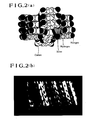
- Figure 2(a) is a model shown in the ac plane of a silver TCNQ molecule with the light blue atoms representing hydrogen, the dark blue nitrogen, the yellow silver and the white carbon.
- Figure 2(b) is an STM image of a film of silver TCNQ on highly oriented pyrolytic graphite (HOPG). The normal orientation of this film is in the ac plane. Note the benzene rings made of white carbon atoms at the center of the molecule model correspond to the bright white stripe in the STM image while the cyano groups, including the dark blue nitrogen atoms correspond to the darker portion of the image.
- HOPG highly oriented pyrolytic graphite
- the electron density of benzene rings is greater than that of the cyano groups and this is demonstrated by the presence of the bright stripe contrasting with the dark blue in the STM image of Fig. 2(b). Note that the colors are not true colors but are colors generated by the computer to enhance the image.
- the switching threshold of the metal TCNQ complex In order to "write" or record data bits for storing in an information storage device, the switching threshold of the metal TCNQ complex, generally in the range of 10 3 - 10 4 V/cm, must be exceeded.
- the Z distance must be constant.
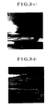
- the threshold field is the electric field between the probe tip and the surface of the substrate. It is equal to the voltage applied to the surface of the film divided by the thickness of the film in addition to the tunneling gap distance and is expressed in volts per centimeter. Applying a field greater than the threshold field drives the reaction of equation 1 to the right causing the electron density to change. The electrons progressively move with time to form increasing amounts of neutral TCNQ and neutral metal. This is called "writing" and is shown in the series of photographs of Figure 3.
- Figure 3a is an STM image of a film of AgTCNQ on a KCl substrate at an X, Y scale of 1000 x 1000 angstroms.
- Figures 3(a), 3(b), 3(c) and 3(d) are images made at 0, 63, 181 and 237 seconds of exposure to the switching field which is approximately 10 5 V/cm.
- the scanning voltage applied to the film for imaging is -2.01 V and the tunneling current is 0.9n A.
- the dark portion is neutral TCNQ and the white portion is neutral silver.
- the feedback circuit shown in Fig. 1 must be turned off if the width is long enough to cause undesirable feedback from feedback control. Note that feedback control is used for "read" mode only. If shorter pulse is used, these feedback problems are minimized. See previously cited U.S. 4,371,883 and 4,652,894 for discussion of pulse width and applied voltage.
- Fig. 3 represents only one location on the film
- the probe tip can be made to move or scan the in X and Y directions recording a plurality of binary data bits. Since a high contrast image is produced, the dark and light areas correspond to 0 and 1 or vice versa.
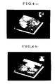
- Fig. 4(a) is a three dimensional STM image of a copper TCNQ film before "writing” and Fig. 4(b) is the image after writing.
- the white spot in Fig. 4(b) is a hillock 4000 angstroms above the surface of the film caused by a pile of electrons which moved in response to the "writing" voltage.
- the "writing" voltage in this particular example is a +2 V pulse.
- the field must be lower than the switching threshold of between 10 3 - 10 4 V/cm and the STM is operated in its normal scanning conditions.
- STM requires at least a bias in the range of 0.1 - 1.0 V to obtain a tunneling current (typically in the range of 0.5 to 5.0 nA or approximately 1 nA).
- the probe tip In the constant height mode, the probe tip is maintained at the Z distance as it scans over the film surface. The current flowing between the tip and the surface is measured with the higher portions of the surface producing the greater current. These higher portions have a greater electron density than the lower portions and thus provide the ability to indicate whether the particular data spot has been "switched". As the STM scans over the surface of the film, it can read a plurality of binary data spots.
- the probe tip In the constant current mode, the probe tip is maintained at a fixed gap distance above the surface of the film. In this way, the current between the probe tip and the surface is always the same but the Z distance changes according to the topography of the film. Changes in the Z distance indicate spots where the electron density has increased or decreased. Again, as the STM scans over the surface of the film, it can read a plurality of binary data spots.
- a +2 V pulse creating an electric field on the order of 10 5 V/cm is applied via an STM probe tip to a 2000 angstroms thick film of copper TCNQ on an HOPG substrate suitably mounted within and connected to an STM.
- This film was deposited on the substrate by the solid-state deposition process. As shown in Fig. 4(b), this produces a high contrast bright data spot approximately 1 micron in diameter and a height of 4000 angstroms above the surface of the film.
- the thus “written” spot is “read” using standard STM scanning condition.
- the voltage applied through the probe tip is +0.302 V.
- the tunneling current is 2.78 nA.
- the visual manifestation of "reading” is the image created by the STM, in this case, Fig. 4(b).
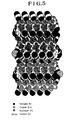
- Fig. 5 shows a model of the crystal structure of Cu(2,5-dimethyl-DCNQI) 2 projected onto the ac plane.
- a periodicity of 3.9 ⁇ along the c axis and a periodicity of 10.8 ⁇ along the axis is recognized.
- the lowest unoccupied molecular orbital (LUMO) of neutral 2,5-dimethyl-DCNQI molecule was calculated by an ab-initio local density function method.
- the LUMO has its highest amplitude on the benzene ring, the cyano groups and the imino groups as shown in the Figure 6.
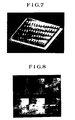
- Figure 7 is an STM image from a terrace parallel to the ac plane of Cu(2,5-dimethyl-DCNQI) 2 at molecular resolution.
- the STM image was obtained at tunneling voltage +100 mV and tunneling current 1.024 nA using the constant current mode.
- This image shows structural periodicities of approximately 11 ⁇ (along the a axis) and approximately 4 ⁇ (along the c axis) that quite agree with the model in Figure 5.
- Figure 8 shows an example of writing spots on the Cu(2,5-dimethyl-DCNQI) 2 single crystal.
- Various size of "written" dark spots were made by varying the voltage applied through the tip from +2V to +4V at desired places.
- the "written” spots are "read” using standard STM scanning condition.
- the voltage applied through the prove tip is +100mV and the tunneling current is 1.024 nA.
- this "writing” can be done to one or two molecules of metal-DCNQI complex as one data bit.
- Figure 9. It shows one data bit stored on the DCNQI molecular column that is shown in Figure 7 by lacking a part of the molecular column.
- this invention is capable of more high density writing in comparison with TCNQ system.
- this invention can be used attaching metal bis-DCNQI complexes on the substrate, it is rather preferable to do it forming thin film on the substrate to have balanced their productivities and performances. In that case, since the shift in electron density is demonstrated by changes in the topography of the charge transfer film, it is necessary for the film to be as smooth as possible.
- An average surface roughness should be less than 500 ⁇ , preferably less than 150 ⁇ and as smooth as possible. Especially, in the case of the constant height mode, it is required to make more smoother in comparison with the case of the constant current mode.
- the system of the invention will operate using charge transfer films deposited by methods such as dipping, spraying, vapor deposition and vacuum deposition, the latter method, vacuum deposition is preferred because it produces the smoothest film.
- the vacuum deposition or solid-state deposition process allows a highly oriented thin film of organometallic charge transfer complex to be deposited.
- the neutral organic portion of the complex is vacuum deposited or sublimed onto a suitable substrate supporting a thin film of the metal portion of the complex.
- the charge transfer complex is formed by heating which initiates an electron transfer reaction between the metal and organic layers.
- the film may also be deposited using a vacuum deposition or solid-state deposition process.
- a film preparation technique using a solution-growth mechanism combined with solid-state processing techniques may be used. This allows DCNQI films to be deposited at room temperature and avoids the problem of having the DCNQI sublimate away before reacting with copper.
- successive depositions of copper or copper(I) iodide and 2,5-dimethyl-N,N'-DCNQI are deposited on a substrate, producing a yellow, double layered film.
- a charge transfer occurs from copper to 2,5-dimethyl-N,N'-DCNQI, producing a blue-black film.
- the DCNQI charge complex film is switched for the writing step by applying an electric field to a very small localized portion of the surface of film using the STM probe tip. This electric field must exceed the threshold field strength for the film.
- a +2 V pulse creating an electric field on the order of 2 x 10 5 V/cm is applied via an STM probe tip to a 1000 angstrom thick film of copper bis 2,5-dimethyl-DCNQI on an HOPG substrate suitably mounted within and connected to an STM.
- the film was deposited on the substrate by the solid-state deposition process and exposed to acetonitrile. This produces a high contrast dark data spot 300 angstroms in diameter and 200 angstroms below the surface of the film.
- the thus "written” spot is "read” using standard STM scanning conditions.
- the voltage applied through the tip is -.041V.
- the tunneling current is 1.024 nA.
- the visual manifestation of "reading” is the image created by the STM.
- the substrate material is required to be flat and atomically or close to atomically smooth. Generally, a greater degree of smoothness is required for small data storage spots than for large one.
- the substrate must also possess sufficient conductivity to insure a stable tunneling current. Examples of suitable substrates are:
- the preferred substrate is HOPG.
- the STM software is available from Park Scientific Instruments.
- the components used in this particular system are also available from Park Scientific Instruments and include: an SPC-400 Scanning Microprobe Central Control Unit, an STM-SU2-210 Scanning Tunneling Microprobe Control Module, an SU2-100 UHV STM Head, an SAI-100 Ambient STM Head, and an SAI/BD2-110 Ambient STM/SFM Base. These are all controlled by a Hewlett-Packard HP 340C Graphic Work Station. However, these may be replaced by any comparable device(s) able to localize an applied voltage to a very small area on the order of nanometer scale and preferably lower. This means that a separate pulse generator may be used to "write".
- the preferred probe tip is electrochemically etched Pt/Ir or Pt alone.
- Another useful tip is made of electrochemically etched W. Au, Ag, Cu and Ni tips may be used.
Landscapes
- Engineering & Computer Science (AREA)
- Chemical & Material Sciences (AREA)
- Nanotechnology (AREA)
- Crystallography & Structural Chemistry (AREA)
- Theoretical Computer Science (AREA)
- Physics & Mathematics (AREA)
- Mathematical Physics (AREA)
- Health & Medical Sciences (AREA)
- Life Sciences & Earth Sciences (AREA)
- General Health & Medical Sciences (AREA)
- Molecular Biology (AREA)
- Semiconductor Memories (AREA)
- Electroluminescent Light Sources (AREA)
Applications Claiming Priority (2)
| Application Number | Priority Date | Filing Date | Title |
|---|---|---|---|
| US924709 | 1992-08-04 | ||
| US07/924,709 US5216661A (en) | 1991-07-22 | 1992-08-04 | Electron density storage device using a stm |
Publications (3)
| Publication Number | Publication Date |
|---|---|
| EP0582290A2 EP0582290A2 (en) | 1994-02-09 |
| EP0582290A3 EP0582290A3 (cg-RX-API-DMAC10.html) | 1994-04-06 |
| EP0582290B1 true EP0582290B1 (en) | 1997-10-29 |
Family
ID=25450590
Family Applications (1)
| Application Number | Title | Priority Date | Filing Date |
|---|---|---|---|
| EP93112498A Expired - Lifetime EP0582290B1 (en) | 1992-08-04 | 1993-08-04 | Electron density storage device |
Country Status (4)
| Country | Link |
|---|---|
| US (1) | US5216661A (cg-RX-API-DMAC10.html) |
| EP (1) | EP0582290B1 (cg-RX-API-DMAC10.html) |
| JP (1) | JPH088476A (cg-RX-API-DMAC10.html) |
| DE (1) | DE69314874T2 (cg-RX-API-DMAC10.html) |
Families Citing this family (9)
| Publication number | Priority date | Publication date | Assignee | Title |
|---|---|---|---|---|
| US6304481B1 (en) | 1994-01-31 | 2001-10-16 | Terastore, Inc. | Method and apparatus for storing data using spin-polarized electrons |
| US5546337A (en) * | 1994-01-31 | 1996-08-13 | Terastore, Inc. | Method and apparatus for storing data using spin-polarized electrons |
| US5446687A (en) * | 1994-01-31 | 1995-08-29 | Terastore, Inc. | Data storage medium for storing data as a polarization of a data magnetic field and method and apparatus using spin-polarized electrons for storing the data onto the data storage medium and reading the stored data therefrom |
| WO1996017345A1 (en) * | 1994-11-29 | 1996-06-06 | Matsushita Electric Industrial Co., Ltd. | Method of recording and reading information and information recording device |
| DE10357044A1 (de) * | 2003-12-04 | 2005-07-14 | Novaled Gmbh | Verfahren zur Dotierung von organischen Halbleitern mit Chinondiiminderivaten |
| US7277314B2 (en) * | 2004-05-27 | 2007-10-02 | Cabot Microelectronics Corporation | Mobile ion memory |
| DE102004037151A1 (de) * | 2004-07-30 | 2006-03-23 | Infineon Technologies Ag | Verfahren zur Bildung von Speicherschichten |
| JP2008059740A (ja) * | 2006-08-24 | 2008-03-13 | Rohm & Haas Co | 情報の書き込みおよび読み込みのための装置および方法 |
| JP5807858B2 (ja) * | 2011-03-24 | 2015-11-10 | 国立大学法人東京工業大学 | 有機薄膜トランジスタ用膜形成用組成物 |
Family Cites Families (5)
| Publication number | Priority date | Publication date | Assignee | Title |
|---|---|---|---|---|
| DE3522232A1 (de) * | 1985-06-21 | 1987-01-02 | Basf Ag | Radikalionensalze |
| DE3789373T2 (de) * | 1986-12-24 | 1994-06-23 | Canon Kk | Aufnahmegerät und Wiedergabegerät. |
| JP2778714B2 (ja) * | 1988-03-02 | 1998-07-23 | 株式会社東芝 | 色素有機薄膜及び色素有機薄膜素子 |
| JP2743213B2 (ja) * | 1990-07-25 | 1998-04-22 | キヤノン株式会社 | 記録及び/又は再生を行なう装置および方法 |
| US5161149A (en) * | 1991-07-22 | 1992-11-03 | The Johns Hopkins University | Electron density storage device and method using STM |
-
1992
- 1992-08-04 US US07/924,709 patent/US5216661A/en not_active Expired - Fee Related
-
1993
- 1993-08-02 JP JP5208184A patent/JPH088476A/ja active Pending
- 1993-08-04 DE DE69314874T patent/DE69314874T2/de not_active Expired - Fee Related
- 1993-08-04 EP EP93112498A patent/EP0582290B1/en not_active Expired - Lifetime
Also Published As
| Publication number | Publication date |
|---|---|
| JPH088476A (ja) | 1996-01-12 |
| EP0582290A2 (en) | 1994-02-09 |
| DE69314874D1 (de) | 1997-12-04 |
| EP0582290A3 (cg-RX-API-DMAC10.html) | 1994-04-06 |
| US5216661A (en) | 1993-06-01 |
| DE69314874T2 (de) | 1998-03-19 |
Similar Documents
| Publication | Publication Date | Title |
|---|---|---|
| US5317152A (en) | Cantilever type probe, and scanning tunnel microscope and information processing apparatus employing the same | |
| JP2859715B2 (ja) | 記録媒体用基板及びその製造方法、記録媒体、記録方法、記録再生方法、記録装置、記録再生装置 | |
| EP0416920B1 (en) | Information processing method and information processing device | |
| EP0334677B1 (en) | Information recording device and information recording and reproducing process | |
| US5481528A (en) | Information processor and method using the information processor | |
| CA2024648C (en) | Accessing method, and information processing method and information processing device utilizing the same | |
| EP0582290B1 (en) | Electron density storage device | |
| US5161149A (en) | Electron density storage device and method using STM | |
| JP3029143B2 (ja) | 情報再生方法 | |
| JPH10289496A (ja) | 情報の記録再生方法及び記録再生装置 | |
| JP2603270B2 (ja) | 記録装置および再生装置 | |
| JP2862352B2 (ja) | 情報処理方法及び情報処理装置 | |
| US7701834B2 (en) | Movable terminal in a two terminal memory array | |
| JP2556520B2 (ja) | 記録装置及び記録法 | |
| JP3029503B2 (ja) | 記録方法および情報処理装置 | |
| JPH01312753A (ja) | 記録再生装置 | |
| JPH05231815A (ja) | 変位素子、及びこれを用いた検出素子、及びこの検出素子を用いた走査型トンネル顕微鏡、原子間力顕微鏡、情報処理装置 | |
| JP4966501B2 (ja) | 走査型プローブメモリ装置 | |
| JP2744341B2 (ja) | アクセス方法及びこれを利用した情報処理方法、情報処理装置 | |
| JP2981786B2 (ja) | 記録媒体、およびそれを用いて記録、再生、消去を行う情報処理装置 | |
| JP2662503B2 (ja) | 記録・再生装置 | |
| JPH05234156A (ja) | プローブ構造体、記録装置、情報検出装置、再生装置及び記録再生装置 | |
| JPH04129043A (ja) | プローブユニット、該プローブユニットを備えた情報処理装置及び情報処理方法 | |
| JPH03173956A (ja) | 記録・再生方法 | |
| JPH04143942A (ja) | トラック形成方法 |
Legal Events
| Date | Code | Title | Description |
|---|---|---|---|
| PUAI | Public reference made under article 153(3) epc to a published international application that has entered the european phase |
Free format text: ORIGINAL CODE: 0009012 |
|
| AK | Designated contracting states |
Kind code of ref document: A2 Designated state(s): DE FR GB NL |
|
| PUAL | Search report despatched |
Free format text: ORIGINAL CODE: 0009013 |
|
| AK | Designated contracting states |
Kind code of ref document: A3 Designated state(s): DE FR GB NL |
|
| RIN1 | Information on inventor provided before grant (corrected) |
Inventor name: VIANDS, CARLA ANN Inventor name: POTEMBER, RICHARD S. Inventor name: YAMAGUCHI, SHOJI, C/O TSUKUBA RESEARCH CENTER |
|
| 17P | Request for examination filed |
Effective date: 19940606 |
|
| RAP1 | Party data changed (applicant data changed or rights of an application transferred) |
Owner name: THE JOHNS HOPKINS UNIVERSITY Owner name: MITSUBISHI CHEMICAL CORPORATION |
|
| GRAG | Despatch of communication of intention to grant |
Free format text: ORIGINAL CODE: EPIDOS AGRA |
|
| 17Q | First examination report despatched |
Effective date: 19961115 |
|
| GRAH | Despatch of communication of intention to grant a patent |
Free format text: ORIGINAL CODE: EPIDOS IGRA |
|
| RAP1 | Party data changed (applicant data changed or rights of an application transferred) |
Owner name: THE JOHNS HOPKINS UNIVERSITY |
|
| GRAH | Despatch of communication of intention to grant a patent |
Free format text: ORIGINAL CODE: EPIDOS IGRA |
|
| GRAA | (expected) grant |
Free format text: ORIGINAL CODE: 0009210 |
|
| AK | Designated contracting states |
Kind code of ref document: B1 Designated state(s): DE FR GB NL |
|
| REF | Corresponds to: |
Ref document number: 69314874 Country of ref document: DE Date of ref document: 19971204 |
|
| ET | Fr: translation filed | ||
| PLBE | No opposition filed within time limit |
Free format text: ORIGINAL CODE: 0009261 |
|
| 26N | No opposition filed | ||
| PGFP | Annual fee paid to national office [announced via postgrant information from national office to epo] |
Ref country code: FR Payment date: 20010718 Year of fee payment: 9 |
|
| PGFP | Annual fee paid to national office [announced via postgrant information from national office to epo] |
Ref country code: DE Payment date: 20010719 Year of fee payment: 9 |
|
| PGFP | Annual fee paid to national office [announced via postgrant information from national office to epo] |
Ref country code: GB Payment date: 20010720 Year of fee payment: 9 |
|
| PGFP | Annual fee paid to national office [announced via postgrant information from national office to epo] |
Ref country code: NL Payment date: 20010723 Year of fee payment: 9 |
|
| REG | Reference to a national code |
Ref country code: GB Ref legal event code: IF02 |
|
| PG25 | Lapsed in a contracting state [announced via postgrant information from national office to epo] |
Ref country code: GB Free format text: LAPSE BECAUSE OF NON-PAYMENT OF DUE FEES Effective date: 20020804 |
|
| PG25 | Lapsed in a contracting state [announced via postgrant information from national office to epo] |
Ref country code: NL Free format text: LAPSE BECAUSE OF NON-PAYMENT OF DUE FEES Effective date: 20030301 Ref country code: DE Free format text: LAPSE BECAUSE OF NON-PAYMENT OF DUE FEES Effective date: 20030301 |
|
| GBPC | Gb: european patent ceased through non-payment of renewal fee |
Effective date: 20020804 |
|
| PG25 | Lapsed in a contracting state [announced via postgrant information from national office to epo] |
Ref country code: FR Free format text: LAPSE BECAUSE OF NON-PAYMENT OF DUE FEES Effective date: 20030430 |
|
| NLV4 | Nl: lapsed or anulled due to non-payment of the annual fee |
Effective date: 20030301 |
|
| REG | Reference to a national code |
Ref country code: FR Ref legal event code: ST |