EP0579226A2 - Transducteur de force et circuit de détection de pression utilisant celui-ci - Google Patents
Transducteur de force et circuit de détection de pression utilisant celui-ci Download PDFInfo
- Publication number
- EP0579226A2 EP0579226A2 EP93111374A EP93111374A EP0579226A2 EP 0579226 A2 EP0579226 A2 EP 0579226A2 EP 93111374 A EP93111374 A EP 93111374A EP 93111374 A EP93111374 A EP 93111374A EP 0579226 A2 EP0579226 A2 EP 0579226A2
- Authority
- EP
- European Patent Office
- Prior art keywords
- voltage
- force
- output
- silicon semiconductor
- temperature
- Prior art date
- Legal status (The legal status is an assumption and is not a legal conclusion. Google has not performed a legal analysis and makes no representation as to the accuracy of the status listed.)
- Granted
Links
- 229910052710 silicon Inorganic materials 0.000 claims abstract description 131
- 239000010703 silicon Substances 0.000 claims abstract description 131
- XUIMIQQOPSSXEZ-UHFFFAOYSA-N Silicon Chemical compound [Si] XUIMIQQOPSSXEZ-UHFFFAOYSA-N 0.000 claims abstract description 130
- 239000004065 semiconductor Substances 0.000 claims abstract description 125
- 239000013078 crystal Substances 0.000 claims abstract description 66
- 230000005540 biological transmission Effects 0.000 claims abstract description 24
- 238000002485 combustion reaction Methods 0.000 claims description 66
- 239000012535 impurity Substances 0.000 claims description 21
- 230000000694 effects Effects 0.000 claims description 11
- 238000005070 sampling Methods 0.000 claims description 9
- 239000000567 combustion gas Substances 0.000 claims description 6
- 239000012212 insulator Substances 0.000 claims description 4
- 238000009529 body temperature measurement Methods 0.000 description 12
- 238000010586 diagram Methods 0.000 description 11
- 230000001419 dependent effect Effects 0.000 description 7
- 238000005516 engineering process Methods 0.000 description 6
- 238000004519 manufacturing process Methods 0.000 description 5
- 238000005259 measurement Methods 0.000 description 4
- 229910052751 metal Inorganic materials 0.000 description 4
- 239000002184 metal Substances 0.000 description 4
- 230000007423 decrease Effects 0.000 description 3
- 238000001514 detection method Methods 0.000 description 3
- 238000009792 diffusion process Methods 0.000 description 2
- 239000013013 elastic material Substances 0.000 description 2
- 230000006870 function Effects 0.000 description 2
- 239000002241 glass-ceramic Substances 0.000 description 2
- 239000000758 substrate Substances 0.000 description 2
- 229910052782 aluminium Inorganic materials 0.000 description 1
- XAGFODPZIPBFFR-UHFFFAOYSA-N aluminium Chemical compound [Al] XAGFODPZIPBFFR-UHFFFAOYSA-N 0.000 description 1
- QVGXLLKOCUKJST-UHFFFAOYSA-N atomic oxygen Chemical compound [O] QVGXLLKOCUKJST-UHFFFAOYSA-N 0.000 description 1
- 230000006835 compression Effects 0.000 description 1
- 238000007906 compression Methods 0.000 description 1
- 238000010276 construction Methods 0.000 description 1
- 230000003247 decreasing effect Effects 0.000 description 1
- 238000006073 displacement reaction Methods 0.000 description 1
- 238000001704 evaporation Methods 0.000 description 1
- 230000008020 evaporation Effects 0.000 description 1
- 239000000463 material Substances 0.000 description 1
- 238000012986 modification Methods 0.000 description 1
- 230000004048 modification Effects 0.000 description 1
- 239000001301 oxygen Substances 0.000 description 1
- 229910052760 oxygen Inorganic materials 0.000 description 1
- 230000004043 responsiveness Effects 0.000 description 1
- 230000000452 restraining effect Effects 0.000 description 1
- 238000000926 separation method Methods 0.000 description 1
- 150000003376 silicon Chemical class 0.000 description 1
- 230000003068 static effect Effects 0.000 description 1
Images


Classifications
-
- G—PHYSICS
- G01—MEASURING; TESTING
- G01L—MEASURING FORCE, STRESS, TORQUE, WORK, MECHANICAL POWER, MECHANICAL EFFICIENCY, OR FLUID PRESSURE
- G01L9/00—Measuring steady of quasi-steady pressure of fluid or fluent solid material by electric or magnetic pressure-sensitive elements; Transmitting or indicating the displacement of mechanical pressure-sensitive elements, used to measure the steady or quasi-steady pressure of a fluid or fluent solid material, by electric or magnetic means
- G01L9/0041—Transmitting or indicating the displacement of flexible diaphragms
- G01L9/0051—Transmitting or indicating the displacement of flexible diaphragms using variations in ohmic resistance
- G01L9/0052—Transmitting or indicating the displacement of flexible diaphragms using variations in ohmic resistance of piezoresistive elements
-
- G—PHYSICS
- G01—MEASURING; TESTING
- G01L—MEASURING FORCE, STRESS, TORQUE, WORK, MECHANICAL POWER, MECHANICAL EFFICIENCY, OR FLUID PRESSURE
- G01L1/00—Measuring force or stress, in general
- G01L1/18—Measuring force or stress, in general using properties of piezo-resistive materials, i.e. materials of which the ohmic resistance varies according to changes in magnitude or direction of force applied to the material
-
- G—PHYSICS
- G01—MEASURING; TESTING
- G01L—MEASURING FORCE, STRESS, TORQUE, WORK, MECHANICAL POWER, MECHANICAL EFFICIENCY, OR FLUID PRESSURE
- G01L9/00—Measuring steady of quasi-steady pressure of fluid or fluent solid material by electric or magnetic pressure-sensitive elements; Transmitting or indicating the displacement of mechanical pressure-sensitive elements, used to measure the steady or quasi-steady pressure of a fluid or fluent solid material, by electric or magnetic means
- G01L9/0041—Transmitting or indicating the displacement of flexible diaphragms
- G01L9/0051—Transmitting or indicating the displacement of flexible diaphragms using variations in ohmic resistance
- G01L9/0058—Transmitting or indicating the displacement of flexible diaphragms using variations in ohmic resistance of pressure sensitive conductive solid or liquid material, e.g. carbon granules
-
- G—PHYSICS
- G01—MEASURING; TESTING
- G01L—MEASURING FORCE, STRESS, TORQUE, WORK, MECHANICAL POWER, MECHANICAL EFFICIENCY, OR FLUID PRESSURE
- G01L9/00—Measuring steady of quasi-steady pressure of fluid or fluent solid material by electric or magnetic pressure-sensitive elements; Transmitting or indicating the displacement of mechanical pressure-sensitive elements, used to measure the steady or quasi-steady pressure of a fluid or fluent solid material, by electric or magnetic means
- G01L9/02—Measuring steady of quasi-steady pressure of fluid or fluent solid material by electric or magnetic pressure-sensitive elements; Transmitting or indicating the displacement of mechanical pressure-sensitive elements, used to measure the steady or quasi-steady pressure of a fluid or fluent solid material, by electric or magnetic means by making use of variations in ohmic resistance, e.g. of potentiometers, electric circuits therefor, e.g. bridges, amplifiers or signal conditioning
- G01L9/06—Measuring steady of quasi-steady pressure of fluid or fluent solid material by electric or magnetic pressure-sensitive elements; Transmitting or indicating the displacement of mechanical pressure-sensitive elements, used to measure the steady or quasi-steady pressure of a fluid or fluent solid material, by electric or magnetic means by making use of variations in ohmic resistance, e.g. of potentiometers, electric circuits therefor, e.g. bridges, amplifiers or signal conditioning of piezo-resistive devices
- G01L9/065—Measuring steady of quasi-steady pressure of fluid or fluent solid material by electric or magnetic pressure-sensitive elements; Transmitting or indicating the displacement of mechanical pressure-sensitive elements, used to measure the steady or quasi-steady pressure of a fluid or fluent solid material, by electric or magnetic means by making use of variations in ohmic resistance, e.g. of potentiometers, electric circuits therefor, e.g. bridges, amplifiers or signal conditioning of piezo-resistive devices with temperature compensating means
-
- Y—GENERAL TAGGING OF NEW TECHNOLOGICAL DEVELOPMENTS; GENERAL TAGGING OF CROSS-SECTIONAL TECHNOLOGIES SPANNING OVER SEVERAL SECTIONS OF THE IPC; TECHNICAL SUBJECTS COVERED BY FORMER USPC CROSS-REFERENCE ART COLLECTIONS [XRACs] AND DIGESTS
- Y10—TECHNICAL SUBJECTS COVERED BY FORMER USPC
- Y10S—TECHNICAL SUBJECTS COVERED BY FORMER USPC CROSS-REFERENCE ART COLLECTIONS [XRACs] AND DIGESTS
- Y10S73/00—Measuring and testing
- Y10S73/04—Piezoelectric
Definitions
- This invention relates to a force transducer which converts a force into an electrical signal using the piezoresistive effect of a semiconductor and also to a pressure detecting circuit using the force transducer, and more particularly to such device and circuit which produces a voltage output corresponding to a force which is applied perpendicularly to the crystal face of a silicon semiconductor while a current flows in the silicon semiconductor.
- Force transducers are widely used in various fields as force detecting sensors and are therefore requested to have such an ability as to measure a force precisely with no influence by the environment.
- the force transducer are used in very severe environment.
- the force transducers are often used under high temperature environment for measuring the pressure in an engine cylinder in order to control the ignition timing of the engine according to the measured pressure.
- the force transducers to be used under such circumstances are required to measure steadily the pressure of combustion gas pressure in the engine with good responsiveness in a wide range of the temperature environment.
- FIGS. 16A and 16B show an example of a prior art force transducer (U.S. Pat. No. 4,833,929); FIG. 16A is a schematic plan view of the sensor, and FIG. 16B is a schematic side view of the sensor.
- This prior art combustion pressure sensor comprises a rectangular planar p-type silicon semiconductor 10 (having a resistivity of 8 ⁇ cm and a thickness of about 200 ⁇ m) with a crystal face (110) 10a on which a force W is to be applied, a force transmission block 30 connected to the crystal face 10a of the silicon semiconductor 10 for transmitting the force W perpendicularly to the crystal face 10a, and a support bed 20 connected to the other face of the silicon semiconductor 10.
- a pair of confronting input electrodes 14, 14' are formed on the silicon semiconductor 10 at an angle of 45 degrees going away anticlockwise from the direction of ⁇ 110> of the crystal.
- a current flows from a power supply to the silicon semiconductor 10 via the input electrodes 14, 14'.
- a pair of confronting output electrodes 12, 12' is formed on the silicon semiconductor 10 at an angle 45 degrees going away anticlockwise from the direction of ⁇ 001> of the crystal.
- the output electrodes 12, 12' output a voltage corresponding to the force W by the piezoresistive effect of the silicon semiconductor. It is therefore possible to measure the force W and hence the combustion gas pressure P (hereinafter called "combustion pressure) by measuring the output voltage.
- I is the current (A) flowing in the silicon semiconductor
- R is the resistance ( ⁇ ) between the input electrodes
- V is the voltage (V) impressed to the silicon semiconductor
- ⁇ 63' is the piezoresistive coefficient (cm2/kg) of the silicon semiconductor of FIGS. 16A and 16B
- ⁇ Z is the compressive stress generated on the crystal face 10a.
- the piezoresistive coefficient ⁇ 63' in Equation 1 may alternatively be expressed by Equation 2 as disclosed in "Use of Piezoresistive Materials in the Measurement of Displacement, Force and Torque" by R.N. Thurston, THE JOURNAL OF THE ACOUSTICAL SOCIETY OF AMERICA, Vol. 29, No. 10, Oct. 1957.
- the piezoresistive coefficient ⁇ 63' can be calculated as about -33X10 ⁇ 6cm2/kg.
- Equation 2 ⁇ 11, ⁇ 12 and ⁇ 44 are the piezoresistive coefficients of a cubic crystal.
- ⁇ 11, ⁇ 12 and ⁇ 44 are the piezoresistive coefficients of a cubic crystal.
- ⁇ 11 6X10 ⁇ 6cm2/kg
- ⁇ 12 -1X10 ⁇ 6cm2/kg
- ⁇ 44 138X10 ⁇ 6cm2/kg.
- a housing having the diaphragm is equipped with, as a pressure detecting means, a force transducer 2000 of FIGS. 16A and 16B having a silicon semiconductor 10, which is known as a highly elastic material, it is possible to realize a combustion pressure sensor which is also able to measure a static pressure.
- the prior force transducer 2000 has the following problems.
- the prior force transducer 2000 requires a pair of input electrodes 14, 14' and a pair of output electrodes 12, 12', both pair to be mounted on the silicon semiconductor 10. If the force transducer 2000 is to be assembled in a housing to constitute a combustion pressure sensor, it requires four lead wires to be connected to the respective electrodes 12, 12', 14, 14'.
- the combustion pressure sensor whose object is to detect the pressure-in-cylinder information more accurately, is mounted directly on an engine. It is a common knowledge that if it is mounted on the engine, the combustion pressure sensor should be left unprotected in a severe environment which has some fear that the sensor might be influenced such as by heat, vibration and external turbulent magnetic field. It can be said that the degree of reliability at the joints which tend to receive heat, vibration, etc. is proportional to the number of lead wires. With this arrangement, because four lead wires and hence many lead wires are used, high-reliability of the joints and low cost of production cannot be achieved. Consequently a force transducer which is simple in structure with the lead wires reduced in number in an effort to secure the high reliability and low cost of production has been desired.
- the force transducer 2000 assembled in the combustion pressure sensor is left unprotected in a high-temperature environment. More particularly, if the engine is operated at a high r.p.m., the temperature of the force transducer 2000 would often reached to 150 o C or higher.
- the silicon semiconductor 10 to be used in the force transducer 2000 is made of a highly elastic material but its resistivity and piezoresistive effect are highly dependent on temperature.
- the silicon semiconductor 10 constituting the force transducer 2000 of FIGS. 16A and 16B has a high resistivity of about 8 ⁇ cm (i.e., a low impurity concentration) and is remarkably dependent on temperature; the temperature dependency is about 0.8 %/ o C in resistivity and about -0.25 %/ o C in piezoresistive effect.
- the resistivity and the piezoresistive effect here are equivalent to the inter-input-electrode resistance R (hereinafter called "the input resistance”) and the piezoresistive effect ⁇ 63' of Equation 1.
- the voltage ⁇ V OLD varies with temperature so that precise detection of the combustion gas pressure P cannot be achieved.
- the prior force transducer 2000 is encountered with a phenomenon that the input resistance is sharply dropped in a range of 150 o C to 200 o C, which results from a physical characteristic that the silicon semiconductor 10 having a resistivity of about 8 ⁇ cm possesses in nature.
- Another object of the invention is to provide a pressure detecting circuit employing the force transducer described in the previous paragraph.
- a force transducer comprising:
- the silicon semiconductor has an SOI (silicon on insulator) structure having a silicon semiconductor layer for detecting the force by utilizing the piezoresistive effect, and the silicon semiconductor layer is a p-type semiconductor controlled to an impurity concentration of about 5X10¹⁸atoms/cm3 or about 2X10²⁰atoms/cm3.
- SOI silicon on insulator
- a pressure detecting circuit comprising:
- the means for measuring the force includes (a) a coefficient memory in which a relation between the offset voltage and a temperature compensation coefficient is stored, (b) a voltage detector for detecting the offset voltage output from the input-output shared electrodes and for detecting the voltage output from the input-output shared electrodes when the force is applied to the crystal face, and (c) a temperature compensator for reading a temperature compensation coefficient corresponding to the detected offset voltage from the coefficient memory and for temperature-compensating the output of the voltage detector to calculate and output a voltage corresponding to the force, whereby the force applied perpendicularly to the crystal face is measured, based on the output of the temperature compensator, with no influence by temperature change.
- a pressure detecting circuit comprising:
- the means for measuring the force includes (a) a coefficient memory in which a relationship between the offset voltage and a temperature compensation coefficient is stored, (b) a voltage detector for detecting the offset voltage output from said voltage divider and for detecting the measured voltage output from said voltage divider when the force is applied on said crystal face, and (c) a temperature compensator for reading a temperature compensation coefficient corresponding to the detected offset voltage from said coefficient memory and for temperature-compensating the output of said voltage detector to calculate and output a voltage corresponding to the force, whereby the force applied perpendicularly to the crystal face is measured, based on the output of said temperature compensator, with no influence by temperature change.
- FIG. 1 shows the primary structure of the force transducer 1000 of this invention.
- the force transducer 1000 comprises a silicon semiconductor 40 having a face 40a of (110), on which a force W is to be applied, or a crystal face equivalent to the face 40a of (110), a pair of confronting input-output shared electrodes 42, 42' mounted on the crystal face 40a of the silicon semiconductor 40 in a direction of ⁇ 110> of the crystal or a direction equivalent to the direction of ⁇ 110>, a force transmission block 60 connected to the crystal face 40a of the silicon semiconductor 40 for transmitting the force W perpendicularly to the crystal face 40a, and a support bed 70 supporting the silicon semiconductor 40 and connected to the silicon semiconductor 40 at a face opposite to the face on which the force transmission block 60 is connected.
- a voltage corresponding to the force W and to be measured will be output from the input-output shared electrodes 42, 42' when the force W is applied perpendicularly to the crystal face 40a of the silicon semiconductor 40 via the force transmission block 60 while a current flows in the silicon semiconductor 40 via the input-output shared electrodes 42, 42'.
- the two input-output shared electrodes 42, 42' are connected to a power supply 100 and a voltage detector 110 via two lead wires 44, 44', to supply current to the silicon semiconductor 40 and detect a voltage created between the two electrodes 42, 42'.
- the combustion pressure sensor employing the force transducer 1000 can measure the combustion pressure precisely with less influence such as by heat, vibration and external turbulent magnetic field.
- the force transducer 1000 utilizes a piezoresistive coefficient ⁇ 13' .
- the piezoresistive coefficient ⁇ 13' of the silicon semiconductor 40 is a piezoresistive coefficient when the direction of detection of voltage and the current flow direction are same and a single-axis stress is generated perpendicularly to such direction.
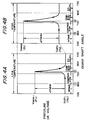
- FIG. 3 represents the piezoresistive coefficient ⁇ 13' when a force W is applied on the crystal face (110) 40a of the p-type silicon semiconductor 40 having a resistivity of 8 ⁇ cm, with the confronting input-output shared electrodes 42, 42' mounted on the silicon semiconductor 40.
- the piezoresistive coefficient ⁇ 13' is represented on a circular graph when it is measured as the direction of location of the input-output shared electrodes 42, 42' is varied throughout the range of 360 degrees.
- the maximal value of the piezoresistive coefficient ⁇ 13' can be obtained if the input-output shared electrodes 42, 42' are formed in the crystal direction ⁇ 110>.
- the piezoresistive coefficient ⁇ 13' in the crystal direction ⁇ 110> can be given by Equation 3, as compared to Equation 2. As is seen from Equation 3, the piezoresistive coefficient ⁇ 13' of the force transducer 1000 is about twice as large as the piezoresistive coefficient ⁇ 63' of the prior force transducer 2000 of FIGS. 16A and 16B.
- the force transducer 1000 is used as a combustion pressure sensor, it is possible to measure the combustion pressure such as of an internal engine precisely, with no influence such as by external turbulent magnetic field.
- the force transducer 1000 when the temperature of the silicon semiconductor 40 varies, the resistance and the piezoresistive coefficient between the input-output shared electrodes 42, 42' also vary sharply depending on the temperature. Consequently, as the ambient temperature of the force transducer 1000 varies, the voltage output of the electrodes 42, 42' fluctuates. The force transducer 1000 therefore requires means for compensating the voltage output according to the ambient temperature.
- the resistance of the silicon semiconductor 40 which constitutes the force transducer 1000 is very dependent on temperature; that is, precise temperature information can be obtained by detecting the resistance value.
- offset voltage means a voltage value between the electrodes 42, 42' of the force transducer 1000 when the pressure is zero.
- the voltage output of the force transducer 1000 is temperature-compensated to calculate the force W.
- FIGS. 4A and 4B show a pressure waveform of reciprocating engine of the four-cycle type in which the pressure varies every moment during individual stages of intake, compression, combustion and exhaust, the pressure values being measured in terms of the inter-electrode voltage values of the force transducer 1000 assembled in the combustion sensor.
- the force transducer 1000 is constant-current-driven by the power supply 100 and the output of the electrodes 42, 42' is detected by a voltage detector 110.
- FIG. 4A shows the pressure waveform from intake 1 to exhaust 1 when the force transducer 1000 is located in a temperature environment lower than the pressure waveform from intake 2 to exhaust 2 of FIG. 4B.
- V off1 and V off2 are the output voltage values (offset voltages) of the force transducer 1000.
- FIG. 5 is a graph of actually measured data, showing the relationship between temperature of the silicon semiconductor 40 and the offset voltage while a constant current flows from the power supply 100 into the silicon semiconductor 40. Specifically, while a constant current of 1 mA flows from the power supply 100 into the p-type silicon semiconductor 40, whose input resistance and resistivity are 1 k ⁇ and about 8 ⁇ cm, via the electrodes 42, 42', the offset voltages were measured by the voltage detector 110, which is connected parallel to the power supply 100, over a temperature range up to 150 o C.
- the offset voltage V off of the silicon semiconductor 40 correlates with temperature. It is therefore possible to obtain precise temperature information by detecting the offset voltage.
- P1 is the maximal pressure in the combustion stage.
- the maximal pressure P1 is set in such a manner that it will be the same value at the time of low-temperature measurement of FIG. 4A and at the time of high-temperature measurement of FIG. 4B.
- the voltage output ⁇ V NEW contained in the output V sens of the force transducer 1000 will be different between at the time of low-temperature measurement and at the time of high-temperature measurement. This is because the input resistance and piezoresistive coefficient ⁇ 13' of the silicon semiconductor 40 are dependent on temperature both at the time of low-temperature measurement and at the time of high-temperature measurement.
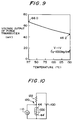
- FIG. 7 is a graph in which the y axis of FIG. 6 is changed from the voltage output to the temperature compensation coefficient based on the voltage output at room temperature, showing the correlation between the temperature and the temperature compensation coefficient while the force transducer 1000 is constant current driven.
- FIG. 8 shows the correlation between the offset voltage and the temperature compensation coefficient while the force transducer 1000 is constant current driven.
- the graph of FIG. 8 may be obtained by exchanging the temperature of FIG. 7 for the offset voltage of FIG. 5.
- the voltage output at the time of high-temperature measurement of FIG. 4B is temperature-compensated.
- the temperature-compensated voltage outputs at the time of low-temperature measurement and at the time of high-temperature measurement are same.
- the pressure detecting circuit comprises the force transducer 1000, a constant current source (i,e, the power supply 100) for supplying a constant current to the input-output shared electrodes 42, 42', and the measuring means for measuring the force W applied perpendicularly to the crystal face 40a of the silicon semiconductor 40 via the force transmission block 60, based on the output voltage of the input-output shared electrodes 42, 42'.
- a constant current source i,e, the power supply 100
- the measuring means for measuring the force W applied perpendicularly to the crystal face 40a of the silicon semiconductor 40 via the force transmission block 60, based on the output voltage of the input-output shared electrodes 42, 42'.
- the measuring means includes the coefficient memory in which the relationship between the offset voltage and the temperature compensation coefficient is stored, the voltage detector for detecting the offset voltage output from the input-output shared electrodes 42, 42' and for detecting the measured voltage output from the input-output shared electrodes 42, 42' when the force W is applied to the crystal face 40a, and the temperature compensator for reading from the coefficient memory the temperature compensation coefficient corresponding to the detected offset voltage and for calculating a temperature-compensated voltage corresponding to the force from the output of the voltage detector and outputting the temperature-compensated voltage.
- the force W applied perpendicularly to the crystal face 40a is measured based on the output of the temperature compensator, with no influence by temperature change.
- Equation 5 The relationship between the voltage V sens , which is obtained from the combustion sensor, and the voltage outputs ⁇ V NEW and V off when the actual pressure P is applied on the force transducer 1000 via the diaphragm of the combustion sensor is given by Equation 5, based on the foregoing algorithms.
- ⁇ V NEW ' (V sens - V off ) ⁇ f(V off ) where f(V off ) is the temperature compensation coefficient to be determined by the offset voltage V off .
- the pressure detecting circuit In the pressure detecting circuit, a constant current is supplied from the power supply 100 to the silicon semiconductor 40 to drive the force transducer 1000. In the absence of the force W applied, the pressure detecting circuit detects the voltage, which is output from the electrodes 42, 42', as the offset voltage V off and reads from the coefficient memory the temperature compensation coefficient f(V off ) corresponding to the offset voltage V off .
- a force W is applied via the force transmission block 60, whereupon the voltage V sens output from the input-output shared electrodes 42, 42' is detected.
- the temperature compensator substitutes the detected voltage V sens , the offset voltage V off and the temperature compensation coefficient f(V off ) in Equation 5 and outputs a temperature-compensated voltage V sens' .
- the obtained voltage V sens' corresponds to the force W always with no influence by the temperature of silicon semiconductor 40, it is possible to obtain the force W precisely based on the temperature-compensated output voltage V sens' , with no influence by temperature change.
- the voltage output is temperature-compensated while the force transducer 1000 is driven by constant current.
- Another pressure detecting circuit comprises a voltage divider 120 in which a resistor 122 is connected in series to the force transducer 1000, a constant voltage source 100 for impressing a constant voltage to the voltage divider 120, and a measuring means for measuring the force W based on the divided voltage output from the voltage divider 120.
- the measuring means includes the coefficient memory in which the relationship between the offset voltage and the temperature compensation coefficient is stored, the voltage detector for detecting the offset voltage output from the voltage divider 120 and for detecting the voltage output from the voltage divider 120 when the force W is applied to the crystal face 40a of the silicon semiconductor 40, and the temperature compensator for reading from the memory the temperature compensation coefficient corresponding to the detected offset voltage and for calculating from the output of the voltage detector a temperature-compensated voltage corresponding to the force W and outputting the temperature-compensated voltage.
- the force W applied perpendicularly to the crystal face 40a is measured based on the output of the temperature compensator, with no influence by temperature change.
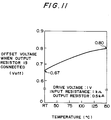
- the silicon semiconductor 40 of the force transducer 1000 is a p-type silicon semiconductor having a resistivity of about 8 ⁇ cm and an input resistance of 1 k ⁇ . If the output resistor 122 has a resistance of 500 ⁇ and the constant voltage source supplies an output voltage of 1 V, the offset voltage, which is measured by a voltmeter 110, of the force transducer 1000 is dependent on temperature as shown in FIG. 11. As is apparent from FIG. 11, since the offset voltage gradually increases along with the temperature rise, it is possible to temperature-compensate the voltage output by utilizing the temperature-dependency of the offset voltage.
- ⁇ V NEW V ⁇ ⁇ 13' ⁇ ⁇ Z
- the voltage output ⁇ V NEW has a negative temperature-dependency gradually decreasing with the temperature rise, shown in FIG. 9. This is because the piezoresistive coefficient ⁇ 13' has a great negative temperature dependency.
- This pressure detecting circuit detects the offset voltage V off of the force transducer 1000 and reads the temperature compensation coefficient corresponding to the offset voltage V off from the coefficient memory. Then when the force W is applied to the force transducer 1000, the pressure detecting circuit detects the voltage output of the force transducer 1000 as a measured voltage and calculates a temperature-compensated voltage corresponding to the force W, based on the measured voltage, the offset voltage and the temperature compensation coefficient.
- the force transducer of this invention it is possible to improve the temperature-dependency of the resistance and piezoresistive coefficient ⁇ 13' of the silicon semiconductor 40 by increasing the impurity concentration and it is also possible to avoid a phenomenon in which the resistance will drop sharply within a range of 150 o C to 200 o C.
- the silicon semiconductor 40 has a thickness of hundreds ⁇ m so that the resistance would be around several ⁇ . If the resistance is small, the constant current source requires a great power supply capacity and the electric power consumption would increase.
- the silicon semiconductor 40 is formed as an SOI (silicon on insulator) and also as a p-type silicon semiconductor layer having an impurity concentration of about 5X10¹⁸atoms/cm3 or about 2X10²⁰atoms/cm3.
- the means for realizing the SOI structure is exemplified by SDB (silicon direct bonding) and SIMOX (separation by implanted oxygen).
- the piezoresistive coefficient decreases while the resistance increases.
- This increase of the resistance causes the increase of the voltage, which is to be impressed to the force transducer as driven by constant current, to cancel the decrease of the piezoresistive coefficient. It is therefore possible to realize a force transducer which would require no compensating circuit and would be free from any current leakage even at a high temperature exceeding 200 o C.
- the force transducer As described above, according to this invention, it is possible to provide a force transducer which is reduced in number of lead wires to cause high reliability and low cost of production in comparison with the prior art. Further, since the voltage output of the force transducer increases twofold, it is possible to measure a force precisely with no influence such as by external turbulent magnetic field. Particularly in the case of a combustion sensor of an internal engine, it is possible to detect information about the pressure to the engine cylinder precisely so that the engine can be controlled more precisely based on the result of detection.
- the silicon semiconductor constituting part of the force transducer is in the SOI structure having a predetermined impurity concentration, it is possible to measure the force accurately even if the force transducer is left unprotected in a severe temperature environment. Particularly in the case of a combustion pressure sensor, it is possible to measure the combustion pressure accurately even under severe high temperature environment, under which the conventional measurement could not be realized.
- the pressure detecting circuit of this invention it is possible to decrease the temperature-dependency of the voltage output of the force transducer so that the force can be measured accurately even under severe temperature environment.
- the pressure detecting circuit of this invention is applied to a combustion pressure sensor to be used under the environment in which temperature fluctuates severely, it is possible to measure the combustion pressure accurately, with no influence by temperature change.
- FIG. 1 shows a force transducer 1000 according to a first embodiment of this invention.
- a silicon semiconductor 40 is a p-type silicon semiconductor having a resistivity of about 8 ⁇ cm, a width w1 of 1.3 mm, a length l1 of 1.3 mm and a thickness of about 100 ⁇ m.
- This silicon semiconductor contains p-type impurities in a concentration of 4X10¹⁸ to 6X10¹⁸atoms/cm3 or 1X10²⁰ to 3X10²⁰atoms/cm3.
- a force transmission block 60 of glass ceramic is fixed centrally to a crystal face (110) 40a of the silicon semiconductor 40 by electrostatic connection.
- the force transmission block 60 is a cube having a width w2 of 1.0 mm, a length l2 of 1.0 mm and a height h2 of 1.0 mm and transmits a force W, which is applied on its top face 60a, perpendicularly to the crystal face 40a of the silicon semiconductor 40.
- a support bed 70 of glass ceramic is fixed by electrostatic connection for supporting the silicon semiconductor 40.
- the support bed 70 has a width w1 of 1.3 mm, a length l1 of 1.3 mm and a height h1 of 1.0 mm.
- a pair of input-output shared electrodes 42, 42' is formed on the crystal face 40a of the silicon semiconductor 40, confronting each other in the direction of ⁇ 110>.
- the electrodes 42, 42' are formed by evaporation of aluminum over the crystal face 40a.
- a power supply 100 and a voltage detector 110 are connected by two lead wires 44, 44', respectively. While a current flows from the power supply 100 to the silicon semiconductor 40 via the electrodes 42, 42', a voltage output from the electrodes 42, 42' is detected by the voltage detector 110.
- FIG. 2 shows a combustion pressure sensor 1100 in which the force transducer 1000 is assembled as a pressure detecting means.
- the combustion pressure sensor 1100 comprises a tubular housing 80 with a metal diaphragm 82 and the force transducer 1000 fixedly mounted in the housing 80.
- the housing 80 is mounted on the wall surface of a cylinder head of a non-illustrated engine in such a manner that a pressure P inside the cylinder is applied on the diaphragm 82.
- the force transducer 1000 is fixedly mounted in the housing 80 using a sealed terminal 90, and the top face 60a of the force transmission block 60 is engageable with the back face of the diaphragm 82.
- the pressure P inside the cylinder is converted into a force W by the metal diaphragm 82, is transmitted to the top face 60a of the force transducer 1000 and is finally applied, as a compressive stress ⁇ Z , on the (110) crystal face 40a of the silicon semiconductor 40.
- a pair of lead pins 92, 92' is mounted on the sealed terminal 90.
- the lead pins 92, 92' are electrically connected at upper ends to the electrodes 42, 42' of the force transducer 1000 by a pair of bonding wires 94, 94' of about 50 ⁇ m in diameter and at lower ends to the power supply 100 and the voltage detector 110 via a pair of lead wires 96, 96', respectively.
- the pressure P is transmitted as a force W to the force transducer 1000 and is converted into a voltage output ⁇ V NEW , which is given by Equation 4, based on the piezoresistive effect of the silicon semiconductor 40.
- the voltage output ⁇ V NEW will be superposed by the offset voltage V off and will be detected, as a voltage V sens , by the voltage detector 110.
- Equation 7,8 and 9 Assuming that a weight (W) of 100 kg is applied on the silicon semiconductor 40 having a resistance R of 1 k ⁇ between the electrodes 42, 42' while a current I of 1 mA flows in the silicon semiconductor 40, ⁇ V NEW , V off and V sens will be given by Equations 7,8 and 9, respectively.
- the offset voltage V off is an inter-electrode voltage when the force W is zero, and ⁇ Z is a stress generated in the silicon semiconductor 40 by the force W.
- a silicon semiconductor for which the piezoresistive coefficient ⁇ 13' can be effectively utilized may have the p-type (111) face, the (211) face or the n-type (100) face; the p-type (110) face is greatest of all.
- the force transducer 1000 can be electrically connected by only two bonding wires 94, 94', which is half the number of wires in the prior art, it is possible to secure a sharply improved degree of reliability resulting from the connected portions by the bonding wires 94, 94'.
- the temperature of the assembled force transducer 1000 will rise up to a high temperature of 150 o C. Since the resistance R and the piezoresistive coefficient ⁇ 13' of the silicon semiconductor 40 are dependent on temperature, the voltage output ⁇ V NEW of the combustion pressure sensor 1100 will vary sharply along with temperature. Due to the temperature-dependency of the resistance of the silicon semiconductor 40, the offset voltage V off of the combustion pressure sensor 1100 also will vary sharply.
- FIG. 12A shows a modified pressure detecting circuit of this embodiment.
- This pressure detecting circuit comprises the force transducer 1000 which is assembled in the combustion pressure sensor 1100, a constant current source 100 for supplying a constant current to the input-output shared electrodes 42, 42' of the force transducer 1000, and a measuring circuit 200 for measuring a force W applied on the force transducer 1000.
- the measuring circuit 200 includes a voltage detector 110, a sampling signal generator 210, registers 220, 222, an arithmetic unit 226, and a memory 224.
- the measuring circuit 200 temperature-compensates the voltage output from the force transducer 1000.
- FIG. 12B is a waveform diagram showing the voltage output from the force transducer 1000 with respect to the pressure P inside the cylinder.
- FIG. 12C is a diagram showing data representing the correlation between offset voltage V off and the temperature compensation coefficient.
- the offset voltage V off and the voltage V sens are voltages obtained at a time T0 and T1 when they are measured in a four-cycle engine as shown in FIG. 12B, i.e., at the time of zero pressure and at the time of maximal pressure, respectively.
- the voltage detector 110 is connected to the sampling signal generator 210 to which the registers 220, 222 and the arithmetic unit 226 are connected.
- the voltage detector 110 which is also connected to the register 220, 222, detects the offset voltage V off and the voltage V sens in synchronism with the sampling signals output from the sampling signal generator 210 at the timing of T0 and T1 and stores the detected values in the respective registers 220, 222.
- the arithmetic unit 226 is connected to the memory 224 in which a map of temperature compensation coefficient f (V off ) corresponding to the offset voltage V off and varying along with temperature is stored.
- the pressure detecting circuit of this embodiment even if the temperature of the combustion pressure sensor 1100 rises by the engine with high pressure and high temperature during the measurement of combustion pressure of the engine when the sensor 1100 is driven by constant current, it is possible to measure precisely the combustion pressure P, which is applied to the diaphragm 82, as temperature-compensated.
- FIG. 13 shows another modified pressure detecting circuit according to a third embodiment.
- the parts or elements corresponding to those of the pressure detecting circuit of FIG. 12A are designated by same reference numerals, and their description is omitted here for clarity.
- a constant voltage source is used as the power supply 100, and the voltage output is outputted to a voltage divider 120.
- the voltage divider 120 comprises a force transducer 1000, and an output resistor 122 connected in series to the force transducer 1000.
- the output resistor 122 is situated at a position substantially same as that of the power supply 100 so that it will scarcely be influenced by any temperature change of the engine.
- a map of temperature compensation coefficient f(V off ) corresponding to the offset voltage V off which varies along with temperature change is stored.
- the temperature compensation coefficient will be different from that in the second embodiment employing the constant current source.
- the voltage detector 110 When sampling signals are output from the sampling signal generator 210 at the timing of T0 and T1, the voltage detector 110 will detect the offset voltage V off and the voltage V sens in synchronism with the sampling signals, and these detected voltage values will be stored in the respective registers 220, 222.
- the pressure detecting circuit of this embodiment even if the constant voltage source is used as the power supply 100, it is possible to measure the pressure, which is applied on the diaphragm of the combustion pressure sensor 1100, accurately, like the second embodiment, with no influence by temperature change.
- the combustion pressure is measured based on the output voltage of the force transducer 1000.
- the temperature-dependency of divided voltage VR' of the output resistor 122 may be utilized, and so it is possible to obtain the same temperature-compensated voltage output.
- FIG. 14B shows the temperature-dependency of the divided voltage VR' obtained while the temperature of the silicon semiconductor 40 is varied under the conditions that the input resistance of the force transducer 1000 including the silicon semiconductor 40 having a resistivity of about 8 ⁇ cm is 1 k ⁇ at room temperature and the resistance value of the output resistor 122 is 500 ⁇ .
- the temperature of the force transducer 1000 assembled in the housing 80 will rise further. Therefore, as long as the silicon semiconductor 40 having a resistivity of 8 ⁇ cm is used, the input resistance will drop sharply at about 200 o C so that measurement of combustion pressure would be impossible.
- the temperature range in which the combustion pressure sensor 1100 is to be used can be widened to the high-temperature side by reducing the resistivity of the silicon semiconductor 40 (i.e., increasing the impurity concentration). By increasing the impurity concentration, it is possible to reduce the temperature-dependency of piezoresistive coefficient.
- the thickness of the silicon semiconductor 40 has a thickness of several hundreds ⁇ m so that the input resistance will be sharply reduced to less than several ⁇ .
- this small-input-resistance force transducer 1000 is driven by a battery of about 10 V
- the battery power supply requires a large current capacitance exceeding several amperes. Consequently, with the ordinary battery power supply, it is difficult to drive the force transducer 1000, and electric power consumption would be massive to cause the temperature of the silicon semiconductor 40 to rise, thus impairing the pressure detecting function.
- the rectangular planar silicon semiconductor 40 should be a thin layer.
- the silicon semiconductor 40 should have a thickness of 0.05 to 1 ⁇ m; for example, if the input resistance is 500 ⁇ and the impurity concentration is about 5X10¹⁸atoms/cm3 , a thickness of around 0.3 ⁇ m is required.
- this thin silicon semiconductor 40 should be formed in an SOI structure.
- the silicon semiconductor layer which has the SOI structure and has a function of detecting a force by utilizing the piezoresistive effect, is driven by constant current to control the impurity concentration to about 5X10¹⁸atoms/cm3 or about 2X10²⁰atoms/cm3 such that the voltage output can be temperature-compensated.
- the silicon semiconductor layer in the SOI structure is realized by using the epitaxial growth technology, the silicon wafer direct bonding (SDB) technology and the SIMOX technology.
- FIG. 15 is a side view showing a modified force transducer 1000 according to another embodiment.
- the parts or elements similar to those of FIG. 1 are designated by same reference numerals, and their description is omitted here for clarity.
- the silicon semiconductor 40 of this embodiment has an SOI structure which includes a substrate silicon wafer 46 having a thickness of 400 ⁇ m and having a crystal face of (110), an oxide film layer 47 having a thickness of about 1 ⁇ m and coated over the substrate silicon wafer 46, and a p-type silicon layer 48 having a thickness of about 0.3 ⁇ m and acting as a device on the oxide film layer 47.
- the silicon layer 48 has a crystal face of (110) and has an impurity concentration of about 5X10¹⁸atoms/cm3.
- the force transducer 1000 of this embodiment has a hemispherical head 62 at the top of the force transmission block 60.
- the contact area of the metal diaphragm 82 of FIG. 2 with the force transmission block 60 is reduced so that direct heat conduction from the high-temperature metal diaphragm 82 to the force transducer 1000 is minimized, thus restraining the force transducer 1000 from temperature rise.
- the force transducer 1000 is accommodated in the housing to constitute a combustion pressure sensor, and the combustion pressure sensor is driven by constant current. It is therefore possible to obtain an accurate voltage output corresponding to the combustion pressure without any voltage output compensator which utilizes the temperature-dependency of the offset voltage like the second and third embodiments.
- this invention is applied to a combustion pressure sensor, but wide applications of the invention in other fields are possible.
Landscapes
- Physics & Mathematics (AREA)
- General Physics & Mathematics (AREA)
- Measuring Fluid Pressure (AREA)
Applications Claiming Priority (2)
| Application Number | Priority Date | Filing Date | Title |
|---|---|---|---|
| JP212082/92 | 1992-07-16 | ||
| JP21208292A JP3166015B2 (ja) | 1992-07-16 | 1992-07-16 | 力変換素子およびこれを用いた圧力検出回路 |
Publications (3)
| Publication Number | Publication Date |
|---|---|
| EP0579226A2 true EP0579226A2 (fr) | 1994-01-19 |
| EP0579226A3 EP0579226A3 (fr) | 1994-02-16 |
| EP0579226B1 EP0579226B1 (fr) | 1997-03-12 |
Family
ID=16616575
Family Applications (1)
| Application Number | Title | Priority Date | Filing Date |
|---|---|---|---|
| EP93111374A Expired - Lifetime EP0579226B1 (fr) | 1992-07-16 | 1993-07-15 | Transducteur de force et circuit de détection de pression utilisant celui-ci |
Country Status (4)
| Country | Link |
|---|---|
| US (1) | US5349873A (fr) |
| EP (1) | EP0579226B1 (fr) |
| JP (1) | JP3166015B2 (fr) |
| DE (1) | DE69308662T2 (fr) |
Cited By (3)
| Publication number | Priority date | Publication date | Assignee | Title |
|---|---|---|---|---|
| EP2169374A2 (fr) | 2008-09-30 | 2010-03-31 | Ngk Spark Plug Co., Ltd. | Appareil résistif de détection de pression |
| EP2169375A3 (fr) * | 2008-09-30 | 2013-09-25 | Ngk Spark Plug Co., Ltd. | Capteur de pression piézorésistif |
| CN105890842A (zh) * | 2015-02-17 | 2016-08-24 | 丰田自动车株式会社 | 压力传感器 |
Families Citing this family (18)
| Publication number | Priority date | Publication date | Assignee | Title |
|---|---|---|---|---|
| JP3317084B2 (ja) * | 1995-03-31 | 2002-08-19 | 株式会社豊田中央研究所 | 力検知素子およびその製造方法 |
| US6433802B1 (en) * | 1998-12-29 | 2002-08-13 | Ncr Corporation | Parallel programming development environment |
| US6860154B2 (en) * | 2001-01-16 | 2005-03-01 | Fujikura Ltd. | Pressure sensor and manufacturing method thereof |
| WO2002057731A1 (fr) * | 2001-01-22 | 2002-07-25 | K-Tech Devices Corp. | Capteur de contrainte |
| DE10203872B4 (de) * | 2002-01-31 | 2004-04-22 | EBM Brosa Messgeräte GmbH & Co. KG | Kraftaufnehmer zum Messen von Druck- bzw. Schubkräften |
| JP2004053344A (ja) * | 2002-07-18 | 2004-02-19 | Tem-Tech Kenkyusho:Kk | 荷重変換型の金属ダイヤフラム圧力センサ |
| DE10232642B4 (de) * | 2002-07-18 | 2006-11-23 | Infineon Technologies Ag | Integrierte Transformatoranordnung |
| US7021154B2 (en) * | 2002-09-24 | 2006-04-04 | Kabushiki Kaisha Toyota Chuo Kenkyusho | Force sensing element |
| US7002227B2 (en) * | 2003-02-28 | 2006-02-21 | Denso Corporation | Pressure detecting device |
| US7256768B2 (en) * | 2003-09-16 | 2007-08-14 | Microsoft Corporation | Computer keyboard with quantitatively force-sensing keys |
| US7123241B2 (en) * | 2003-09-16 | 2006-10-17 | Microsoft Corporation | Quantitatively force-sensing computer keyboard |
| JP4708711B2 (ja) * | 2004-02-03 | 2011-06-22 | 株式会社デンソー | 圧力センサ |
| JP5108601B2 (ja) * | 2008-04-16 | 2012-12-26 | 日本特殊陶業株式会社 | 燃焼圧力センサ付きグロープラグ |
| JP4810690B2 (ja) | 2008-11-11 | 2011-11-09 | 株式会社豊田中央研究所 | 力検知素子 |
| US7962307B2 (en) * | 2009-02-23 | 2011-06-14 | General Electric Company | Integrated apparatus for measuring static pressure |
| DE102011105756A1 (de) * | 2011-01-28 | 2012-08-02 | Kaufbeurer Mikrosysteme Wiedemann Gmbh | Elektrische Messeinrichtung zur Kraft- und/oder Druckmessung |
| JP5761536B2 (ja) * | 2013-04-24 | 2015-08-12 | 横河電機株式会社 | 力変換素子 |
| DE102015104410B4 (de) * | 2015-03-24 | 2018-09-13 | Tdk-Micronas Gmbh | Drucksensor |
Citations (2)
| Publication number | Priority date | Publication date | Assignee | Title |
|---|---|---|---|---|
| JPS62175631A (ja) * | 1986-01-30 | 1987-08-01 | Mitsubishi Electric Corp | プログラム可能な半導体圧力センサ |
| EP0352773A2 (fr) * | 1988-07-26 | 1990-01-31 | Kabushiki Kaisha Toyota Chuo Kenkyusho | Capteur de pression Si monocrystallin piezoresistif |
Family Cites Families (7)
| Publication number | Priority date | Publication date | Assignee | Title |
|---|---|---|---|---|
| US3351786A (en) * | 1965-08-06 | 1967-11-07 | Univ California | Piezoelectric-semiconductor, electromechanical transducer |
| JPS5148729B2 (fr) * | 1971-09-25 | 1976-12-22 | ||
| US4320664A (en) * | 1980-02-25 | 1982-03-23 | Texas Instruments Incorporated | Thermally compensated silicon pressure sensor |
| US4703658A (en) * | 1986-06-18 | 1987-11-03 | Motorola, Inc. | Pressure sensor assembly |
| JPH0682847B2 (ja) * | 1987-07-31 | 1994-10-19 | 株式会社豊田中央研究所 | 力変換素子 |
| US4771639A (en) * | 1987-09-02 | 1988-09-20 | Yokogawa Electric Corporation | Semiconductor pressure sensor |
| JPH03148028A (ja) * | 1989-11-02 | 1991-06-24 | Matsushita Electric Ind Co Ltd | 圧電型圧力センサ |
-
1992
- 1992-07-16 JP JP21208292A patent/JP3166015B2/ja not_active Expired - Fee Related
-
1993
- 1993-07-15 EP EP93111374A patent/EP0579226B1/fr not_active Expired - Lifetime
- 1993-07-15 DE DE69308662T patent/DE69308662T2/de not_active Expired - Fee Related
- 1993-07-16 US US08/092,480 patent/US5349873A/en not_active Expired - Lifetime
Patent Citations (2)
| Publication number | Priority date | Publication date | Assignee | Title |
|---|---|---|---|---|
| JPS62175631A (ja) * | 1986-01-30 | 1987-08-01 | Mitsubishi Electric Corp | プログラム可能な半導体圧力センサ |
| EP0352773A2 (fr) * | 1988-07-26 | 1990-01-31 | Kabushiki Kaisha Toyota Chuo Kenkyusho | Capteur de pression Si monocrystallin piezoresistif |
Non-Patent Citations (3)
| Title |
|---|
| PATENT ABSTRACTS OF JAPAN vol. 12, no. 19 (P-657)(2866) 21 January 1988 & JP-A-62 175 631 (MITSUBISHI) 1 August 1987 * |
| SENSORS AND ACTUATORS A vol. 27, no. 1/3 , May 1991 , LAUSANNE CH pages 801 - 807 H.J.C.M. VAN GESTEL ET AL 'On-Chip Piezoresistiv Stress Measurement in 3 Directions' * |
| SENSORS AND ACTUATORS vol. 13, no. 1 , January 1988 , LAUSANNE CH pages 53 - 62 I. IGARASHI 'Semiconductive Dynamic Sensors' * |
Cited By (6)
| Publication number | Priority date | Publication date | Assignee | Title |
|---|---|---|---|---|
| EP2169374A2 (fr) | 2008-09-30 | 2010-03-31 | Ngk Spark Plug Co., Ltd. | Appareil résistif de détection de pression |
| EP2169374A3 (fr) * | 2008-09-30 | 2013-09-25 | Ngk Spark Plug Co., Ltd. | Appareil résistif de détection de pression |
| EP2169375A3 (fr) * | 2008-09-30 | 2013-09-25 | Ngk Spark Plug Co., Ltd. | Capteur de pression piézorésistif |
| CN105890842A (zh) * | 2015-02-17 | 2016-08-24 | 丰田自动车株式会社 | 压力传感器 |
| EP3059565A1 (fr) * | 2015-02-17 | 2016-08-24 | Toyota Jidosha Kabushiki Kaisha | Capteur de pression |
| CN105890842B (zh) * | 2015-02-17 | 2019-03-01 | 丰田自动车株式会社 | 压力传感器 |
Also Published As
| Publication number | Publication date |
|---|---|
| DE69308662D1 (de) | 1997-04-17 |
| US5349873A (en) | 1994-09-27 |
| JP3166015B2 (ja) | 2001-05-14 |
| DE69308662T2 (de) | 1997-10-16 |
| EP0579226A3 (fr) | 1994-02-16 |
| JPH0634455A (ja) | 1994-02-08 |
| EP0579226B1 (fr) | 1997-03-12 |
Similar Documents
| Publication | Publication Date | Title |
|---|---|---|
| EP0579226B1 (fr) | Transducteur de force et circuit de détection de pression utilisant celui-ci | |
| US4320664A (en) | Thermally compensated silicon pressure sensor | |
| EP0352773B1 (fr) | Capteur de pression Si monocrystallin piezoresistif | |
| US4430895A (en) | Piezoresistive accelerometer | |
| US5681997A (en) | Excitation of polysilicon based piezoresistive pressure sensors | |
| US4373399A (en) | Semiconductor strain gauge transducer | |
| JPH0546488B2 (fr) | ||
| EP0470744B1 (fr) | Palpeur de force électrochimique | |
| US6487898B1 (en) | Engine cylinder pressure sensor with thermal compensation element | |
| US5528940A (en) | Process condition detecting apparatus and semiconductor sensor condition detecting circuit | |
| US3213681A (en) | Shear gauge pressure-measuring device | |
| US3392576A (en) | Semiconductor transducers | |
| JPS59158566A (ja) | 半導体加速度センサ | |
| JPH06296032A (ja) | 力変換素子 | |
| JPH06201492A (ja) | 力変換素子 | |
| JPH041472Y2 (fr) | ||
| SU960559A2 (ru) | Датчик давлени | |
| JPH0455542B2 (fr) | ||
| JPH10332519A (ja) | 圧力センサの特性測定装置 | |
| JPH0610641B2 (ja) | 高温流体用圧力センサ | |
| JPH04174319A (ja) | 物理量検出器 | |
| SU934257A1 (ru) | Полупроводниковый тензопреобразователь | |
| US3298233A (en) | Probe transducer | |
| Castle | temperature compensated silicon strain transducer | |
| SU1247693A1 (ru) | Полупроводниковое измерительное устройство |
Legal Events
| Date | Code | Title | Description |
|---|---|---|---|
| PUAI | Public reference made under article 153(3) epc to a published international application that has entered the european phase |
Free format text: ORIGINAL CODE: 0009012 |
|
| PUAL | Search report despatched |
Free format text: ORIGINAL CODE: 0009013 |
|
| AK | Designated contracting states |
Kind code of ref document: A2 Designated state(s): DE FR GB |
|
| AK | Designated contracting states |
Kind code of ref document: A3 Designated state(s): DE FR GB |
|
| 17P | Request for examination filed |
Effective date: 19940120 |
|
| 17Q | First examination report despatched |
Effective date: 19951109 |
|
| GRAG | Despatch of communication of intention to grant |
Free format text: ORIGINAL CODE: EPIDOS AGRA |
|
| GRAH | Despatch of communication of intention to grant a patent |
Free format text: ORIGINAL CODE: EPIDOS IGRA |
|
| GRAH | Despatch of communication of intention to grant a patent |
Free format text: ORIGINAL CODE: EPIDOS IGRA |
|
| GRAA | (expected) grant |
Free format text: ORIGINAL CODE: 0009210 |
|
| AK | Designated contracting states |
Kind code of ref document: B1 Designated state(s): DE FR GB |
|
| REF | Corresponds to: |
Ref document number: 69308662 Country of ref document: DE Date of ref document: 19970417 |
|
| ET | Fr: translation filed | ||
| PLBE | No opposition filed within time limit |
Free format text: ORIGINAL CODE: 0009261 |
|
| STAA | Information on the status of an ep patent application or granted ep patent |
Free format text: STATUS: NO OPPOSITION FILED WITHIN TIME LIMIT |
|
| 26N | No opposition filed | ||
| PGFP | Annual fee paid to national office [announced via postgrant information from national office to epo] |
Ref country code: GB Payment date: 19980706 Year of fee payment: 6 |
|
| PGFP | Annual fee paid to national office [announced via postgrant information from national office to epo] |
Ref country code: FR Payment date: 19980709 Year of fee payment: 6 |
|
| PGFP | Annual fee paid to national office [announced via postgrant information from national office to epo] |
Ref country code: DE Payment date: 19980724 Year of fee payment: 6 |
|
| PG25 | Lapsed in a contracting state [announced via postgrant information from national office to epo] |
Ref country code: GB Free format text: LAPSE BECAUSE OF NON-PAYMENT OF DUE FEES Effective date: 19990715 |
|
| PG25 | Lapsed in a contracting state [announced via postgrant information from national office to epo] |
Ref country code: FR Free format text: THE PATENT HAS BEEN ANNULLED BY A DECISION OF A NATIONAL AUTHORITY Effective date: 19990731 |
|
| GBPC | Gb: european patent ceased through non-payment of renewal fee |
Effective date: 19990715 |
|
| PG25 | Lapsed in a contracting state [announced via postgrant information from national office to epo] |
Ref country code: DE Free format text: LAPSE BECAUSE OF NON-PAYMENT OF DUE FEES Effective date: 20000503 |
|
| REG | Reference to a national code |
Ref country code: FR Ref legal event code: ST |