EP0352773A2 - Capteur de pression Si monocrystallin piezoresistif - Google Patents
Capteur de pression Si monocrystallin piezoresistif Download PDFInfo
- Publication number
- EP0352773A2 EP0352773A2 EP89113807A EP89113807A EP0352773A2 EP 0352773 A2 EP0352773 A2 EP 0352773A2 EP 89113807 A EP89113807 A EP 89113807A EP 89113807 A EP89113807 A EP 89113807A EP 0352773 A2 EP0352773 A2 EP 0352773A2
- Authority
- EP
- European Patent Office
- Prior art keywords
- single crystal
- diaphragm
- pressure
- seat
- crystal
- Prior art date
- Legal status (The legal status is an assumption and is not a legal conclusion. Google has not performed a legal analysis and makes no representation as to the accuracy of the status listed.)
- Granted
Links
Images


Classifications
-
- G—PHYSICS
- G01—MEASURING; TESTING
- G01L—MEASURING FORCE, STRESS, TORQUE, WORK, MECHANICAL POWER, MECHANICAL EFFICIENCY, OR FLUID PRESSURE
- G01L19/00—Details of, or accessories for, apparatus for measuring steady or quasi-steady pressure of a fluent medium insofar as such details or accessories are not special to particular types of pressure gauges
- G01L19/14—Housings
- G01L19/142—Multiple part housings
-
- G—PHYSICS
- G01—MEASURING; TESTING
- G01L—MEASURING FORCE, STRESS, TORQUE, WORK, MECHANICAL POWER, MECHANICAL EFFICIENCY, OR FLUID PRESSURE
- G01L1/00—Measuring force or stress, in general
- G01L1/18—Measuring force or stress, in general using properties of piezo-resistive materials, i.e. materials of which the ohmic resistance varies according to changes in magnitude or direction of force applied to the material
-
- G—PHYSICS
- G01—MEASURING; TESTING
- G01L—MEASURING FORCE, STRESS, TORQUE, WORK, MECHANICAL POWER, MECHANICAL EFFICIENCY, OR FLUID PRESSURE
- G01L19/00—Details of, or accessories for, apparatus for measuring steady or quasi-steady pressure of a fluent medium insofar as such details or accessories are not special to particular types of pressure gauges
- G01L19/0061—Electrical connection means
- G01L19/0084—Electrical connection means to the outside of the housing
-
- G—PHYSICS
- G01—MEASURING; TESTING
- G01L—MEASURING FORCE, STRESS, TORQUE, WORK, MECHANICAL POWER, MECHANICAL EFFICIENCY, OR FLUID PRESSURE
- G01L19/00—Details of, or accessories for, apparatus for measuring steady or quasi-steady pressure of a fluent medium insofar as such details or accessories are not special to particular types of pressure gauges
- G01L19/06—Means for preventing overload or deleterious influence of the measured medium on the measuring device or vice versa
- G01L19/0627—Protection against aggressive medium in general
- G01L19/0645—Protection against aggressive medium in general using isolation membranes, specially adapted for protection
-
- G—PHYSICS
- G01—MEASURING; TESTING
- G01L—MEASURING FORCE, STRESS, TORQUE, WORK, MECHANICAL POWER, MECHANICAL EFFICIENCY, OR FLUID PRESSURE
- G01L19/00—Details of, or accessories for, apparatus for measuring steady or quasi-steady pressure of a fluent medium insofar as such details or accessories are not special to particular types of pressure gauges
- G01L19/14—Housings
- G01L19/147—Details about the mounting of the sensor to support or covering means
-
- G—PHYSICS
- G01—MEASURING; TESTING
- G01L—MEASURING FORCE, STRESS, TORQUE, WORK, MECHANICAL POWER, MECHANICAL EFFICIENCY, OR FLUID PRESSURE
- G01L9/00—Measuring steady of quasi-steady pressure of fluid or fluent solid material by electric or magnetic pressure-sensitive elements; Transmitting or indicating the displacement of mechanical pressure-sensitive elements, used to measure the steady or quasi-steady pressure of a fluid or fluent solid material, by electric or magnetic means
- G01L9/0041—Transmitting or indicating the displacement of flexible diaphragms
- G01L9/0042—Constructional details associated with semiconductive diaphragm sensors, e.g. etching, or constructional details of non-semiconductive diaphragms
-
- G—PHYSICS
- G01—MEASURING; TESTING
- G01L—MEASURING FORCE, STRESS, TORQUE, WORK, MECHANICAL POWER, MECHANICAL EFFICIENCY, OR FLUID PRESSURE
- G01L9/00—Measuring steady of quasi-steady pressure of fluid or fluent solid material by electric or magnetic pressure-sensitive elements; Transmitting or indicating the displacement of mechanical pressure-sensitive elements, used to measure the steady or quasi-steady pressure of a fluid or fluent solid material, by electric or magnetic means
- G01L9/0041—Transmitting or indicating the displacement of flexible diaphragms
- G01L9/0051—Transmitting or indicating the displacement of flexible diaphragms using variations in ohmic resistance
- G01L9/0052—Transmitting or indicating the displacement of flexible diaphragms using variations in ohmic resistance of piezoresistive elements
-
- Y—GENERAL TAGGING OF NEW TECHNOLOGICAL DEVELOPMENTS; GENERAL TAGGING OF CROSS-SECTIONAL TECHNOLOGIES SPANNING OVER SEVERAL SECTIONS OF THE IPC; TECHNICAL SUBJECTS COVERED BY FORMER USPC CROSS-REFERENCE ART COLLECTIONS [XRACs] AND DIGESTS
- Y10—TECHNICAL SUBJECTS COVERED BY FORMER USPC
- Y10S—TECHNICAL SUBJECTS COVERED BY FORMER USPC CROSS-REFERENCE ART COLLECTIONS [XRACs] AND DIGESTS
- Y10S73/00—Measuring and testing
- Y10S73/04—Piezoelectric
Definitions
- the present invention relates to a semiconductor pressure transducer and, more particularly, to a semiconductor pressure transducer for converting the pressure applied to a diaphragm into an electric signal and outputting the electric signal corresponding to the pressure.
- a semiconductor pressure transducer is widely used in various fields as a sensor for detecting pressure. Such a pressure transducer is required to have a capability of accurately measuring pressure without being influenced by the ambience.
- a semiconductor pressure transducer is often used under a severe circumstance.
- some semiconductor pressure transducers have recently been used for measuring the pressure of a combustion gas in the cylinder of an internal combustion engine.
- a semiconductor pressure transducer used under such a severe circumstance is naturally required to measure the compression force applied thereto with good responsiveness and high reliability without being influenced by magnetic and electric noise in the ambience.
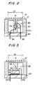
- Fig. 2 shows an example of a conventional strain-gauge transducer.
- This pressure transducer is composed of a diaphragm 10 provided with a cylindrical supporting portion 10a which is secured to a supporting plate 40, and a pressure detector 20 for detecting the pressure P applied to the surface 12 of the diaphragm 10.
- the pressure detector 20 includes a square pillar-shaped strain generator 30 which is erected on the supporting plate 40 such that the upper end thereof is in contact with the center of the back surface of the diaphragm 10 and a semiconductor strain gauge 34 pasted on each side surface of the strain generator 30 by an adhesive 32.
- the pressure P applied to the diaphragm 10 is transmitted to the strain generator 30 in the form of the compression force W (W ⁇ ⁇ r2 ⁇ P ⁇ k1, wherein k1 represents the conversion efficiency of the diaphragm 10).
- the strain produced on the strain generator 30 on the basis of the compression force W is detected by each strain gauge 34, and the voltage signal output from each strain gauge 34 is output through lead wires 36.
- Such a conventional strain-gauge pressure transducer has the following problems.
- the semiconductor strain gauge 34 is pasted on each side surface of the strain generator 30 by an adhesive in order to reduce the deleterious influence of the resistance of the semiconductor strain gauge which is varied with change of temperature on the detection characteristic, and these plurality of semiconductor strain gauges are connected with each other in such a manner as to constitute a Wheatstone bridge circuit.
- the manufacturing process of the pressure transducer has therefore become complicated and, hence, the pressure transducer produced is expensive.
- Fig. 3 shows an example of a conventional piezoelectric pressure transducer.
- This pressure transducer is provided with the pressure detector 20 so designed that the pressure P applied to the diaphragm 10 acts on a piezoelectric element 60 mounted on the supporting plate 40 as the compression force W through a transmitting means 50.
- the piezoelectric element 60 is so constituted as to output the voltage corresponding to the pressure P from electrodes 62 provided on both sides of the piezoelectric element 60 through lead wires 64.
- a charge amplifier is used for effecting an impedance conversion in the vicinity of the piezoelectric element 60, thereby leading the voltage to the outside.
- the charge amplifier is too expensive to be used together with the pressure transducer and this measure cannot be said the essential solution of the above-described problems.
- the strain-gauge pressure transducer has a problem in the heat resistance of the adhesive 32 at a high temperature, while the piezoelectric pressure transducer has a problem in reliability of the dielectic constant of the piezoelectric element 60 which greatly varies with change of temperature.
- the present invention provides a pressure transducer comprising: a diaphragm; and a pressure detector; the pressure detector including: an Si single crystal which is so formed as to have a crystal face of ⁇ 110 ⁇ as the surface to which a compression force is applied, and which is attached to the pressure detector such that the crystal face is parallel to the diaphragm; a plurality of electrodes which consist of a first pair of opposing electrodes provided on the Si single crystal in the direction having an angle of 45 degrees with the direction of ⁇ 001> on the crystal face of ⁇ 110 ⁇ and a second pair of opposing electrodes provided on the Si single crystal in the direction having an angle of 45 degrees with the direction of ⁇ 110> of the Si single crystal, either of the first or second pair of electrodes serving as output electrodes and the other pair serving as input electrodes; a composite seat with one end portion and the other end portion being made of different materials from each other, the one end portion being bonded to the crystal face of ⁇ 110 ⁇ of the Si single crystal and the other end portion
- a Wheatstone bridge circuit is constituted by a plurality of semiconductor strain gauges in order to reduce the deleterious influence of a change in the resistance caused by a change in the temperature of the semiconductor strain gauges on the characteristics.
- the first point aimed at in the present invention is to constitute a plurality of strain gauges by one Si single crystal in place of the Wheatstone bridge circuit constituted by such a plurality of semiconductor strain gauges in the related art.
- a pair of opposing output electrodes and a pair of opposing input electrodes are provided on one Si single crystal in such a manner as to intersect each other, preferably such as to be orthogonal to each other.
- Such a structure can solve one of the above-described problems in the related art by reducing the deleterious influence of a temperature change on the characteristics for the reasons which will be described later.
- the second point aimed at by the present invention is to adopt a novel system for detecting pressure in which a compression force is applied perpendicularly to the crystal face of the Si single crystal and the compression force is detected by utilizing the piezoresistive effect of the Si single crystal based on the compression force.
- a conventional pressure transducer is provided with a plurality of strain gauges pasted to the side surfaces of a a strain generator by an adhesive, and detects a compression force as the compression strain of the strain generator.
- the compression strain of the strain gauge is therefore transmitted to each strain gauge through the adhesive, so that the transducer is susceptible to deleterious influence of the adhesive such as creep and hysteresis, thereby lowering the reliability.
- a quite novel structure is adopted in which one crystal surface of an Si single crystal is bonded to a seat and the other to a support base, and a compression force is applied perpendicularly to the crystal face of the Si single crystal.
- the Si single crystal is preferably bonded with the seat and the support base not by an adhesive but by electrostatic bonding which is disclosed in, for example, Japanese Patent Publication No. 28747/1978.
- the present inventors investigated the crystal surface of an Si single crystal which provides a large piezoresistive coefficient ⁇ 63′. As a result, it has been found that it is necessary to form an Si single crystal so as to have a crystal face of ⁇ 110 ⁇ as the surface to which a compression force is applied.
- the efficiency of an Si single crystal is greatly reduced when it is used under a high-temperature circumstance.
- the degree of reduction is different depend necessarilying upon the source and the density of the impurity of the Si single crystal.
- the resistance gradually rises in a temperature range between the vicinity of room temperature and about 250°C without a sudden change, but when the temperature has reached to 250°C, the resistance rapidly decreases. Accordingly, a semiconductor pressure transducer using such an Si single crystal cannot be used under a high-temperature circumstance as it is.
- the present inventors studied a measure for preventing the conduction of heat from the diaphragm to which the pressure P is applied to the Si single crystal in case of use under a high-temperature circumstance.
- the seat since one end of the seat is bonded to the Si single crystal, it is preferable to form the seat from a material having a thermal expansion coefficient approximate to that of the Si single crystal. On the other hand, since the other end of the seat is in contact with the diaphragm, it is preferable to form this portion from a material excellent in mechanical strength and thermal insulation property.
- the present inventors have formed the portion of the seat which is to be bonded to the Si single crystal from an electrically insulating material having a thermal expansion coefficient approximate to that of the Si single crystal, and the portion of the seat which is to be brought into contact with the diaphragm from a material having a more excellent mechanical strength or thermal insulation property than the material used for the portion which is bonded to the Si single crystal.
- the seat itself is formed as a composite seat consisting of a combination of two kinds of materials, as described above, when the pressure of high-temperature and high-pressure fluid such as combustion gas in the cylinder of an internal combustion engine is measured, the heat transmitted to the diaphragm is alleviated by the seat and does not act on the Si single crystal as a high temperature.
- the Si single crystal is therefore capable of outputting the voltage corresponding to the pressure P applied to the diaphragm without being influenced by the ambient temperature.
- a compression force sometimes locally acts on the diaphragm due to local contact in accordance with the state of the bonded area. In this case, the seat is sometimes plastically deformed or broken.
- the material having excellent mechanical strength for this portion as described above, the seat is not broken due to the local contact of the portion of the seat bonded to the diaphragm, thereby enabling accurate measurement of the pressure P.
- the seat itself is formed from a composite material.
- a pressure transmitting portion formed of a material having an excellent thermal insulation property or an excellent mechanical strength at the portion of the diaphragm which is to be brought into contact with the seat. This structure also enables the stable measurement of the pressure of high-temperature and high-pressure fluid.
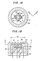
- Fig. 1 shows a semiconductor pressure transducer according to the present invention.
- the pressure transducer is composed of a cylindrical diaphragm 10 having a radius of r secured to a supporting plate 40, and a pressure detector 20 which is secured to the supporting plate 40 for detecting the pressure P applied to the surface 12 of the diaphragm 10 and converting the pressure P into an electric signal.
- the surface 12 of the diaphragm 10 is ordinarily exposed to the fluid. It is therefore preferable that the supporting plate 40 is formed from a thermally and electrically insulating material so as to prevent the heat transmitted from the high-temperature and high-pressure fluid to the diaphragm 10 from being transmitted to the pressure detector 20 through the supporting plate 40.
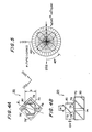
- Fig. 4 shows an example of the concrete structure of the pressure detector 20.
- the pressure detector 20 includes an Si single crystal 70 so formed as to have a crystal face 72 of (110) as the surface to which a compression force is applied, a seat 80 bonded to the crystal face 72 of (110) of the Si single crystal 70 and transmitting the pressure P applied to the diaphragm 10 perpendicularly to the crystal face 72 as the compression force W, and a support base 90 bonded to the other crystal face 74 of the Si single crystal 70 and supporting the Si single crystal 70.
- the support base 90 of the pressure detector 20 is secured to the supporting plate 40, and the seat 80 is in contact with the central portion 14 of the back surface of the diaphragm 10.
- the seat 80 and the support base 90 are preferably electrically insulated from the Si single crystal 70 and are preferably formed from a material having a thermal expansion coefficient approximate to that of the Si single crystal 70.
- the seat 80 and the support base 90 are preferably bonded to the Si single crystal 70 without using an adhesive.
- an electrostatic bonding method or a direct bonding method disclosed in Japanese Patent Publication No. 17869/1964 may be adopted.
- the Si single crystal 70 is provided with a first pair of opposing electrodes 76, 76′ in the direction having an angle of 45 degrees with the direction of [001] and a second pair of opposing electrodes 78, 78′ in the direction having an angle of 45 degrees with the direction of [1 1 0]. Either of the first or second pair of electrodes are used as output electrodes and the other pair as input electrodes.
- ⁇ V b ⁇ ⁇ ⁇ J2 ⁇ ⁇ 63′ ⁇ ⁇ Z ⁇ k1 (1) wherein ⁇ represents the resistivity of the Si single crystal 70, J2 a current density, and ⁇ 63′ a piezoresistive coefficient.
- the feature of the present invention lies in that the Si single crystal 70 is so formed that the piezoresistive coefficient ⁇ 63′ takes a sufficiently large value in order to output from the output voltages 76, 76′ the voltage ⁇ V which corresponds to the compression force.
- the present inventors calculated the piezoresistive coefficient ⁇ 63′, which is essential for obtaining the voltage ⁇ V from the Si single crystal 70, while varying the direction in which the electrodes are provided on the four Si single crystals having typical crystal faces (100), (110), (111) and (211), respectively.
- the piezoresistive coefficient ⁇ 63′ becomes zero irrespective of the direction in which the electrodes are provided, while in the case of (110), when the electrodes are provided in the direction having an angle of 45 degrees with the direction of [001] or [1 1 0], the maximum piezoresistive coefficients ⁇ 63′ having the same absolute value is obtained.
- Fig. 5 shows the results of the calculation of the piezoresistive coefficient ⁇ 63′ of a p-type Si single crystal having a crystal face of (110) and a resistivity of 7.8 ⁇ cm. It is clear that when the output electrodes 76, 76′ are provided in the direction having an angle of 45 degrees with the direction of [001] and the input electrodes 78, 78′ are provided in the direction having an angle of 45 degrees with the direction of [1 1 0], the maximum piezoresistive coefficient ⁇ 63′ is obtained.
- Table 1 shows the crystal faces which are equivalent to the crystal face (110) of the Si single crystal 70 and the directions of crystallization which are equivalent to the directions of [001] and [1 1 0].
- Table 1 shows the crystal faces which are equivalent to the crystal face (110) of the Si single crystal 70 and the directions of crystallization which are equivalent to the directions of [001] and [1 1 0].
- the crystal face equivalent to the crystal face (110) is represented by ⁇ 110 ⁇ and the directions of crystallization which are equivalent to [001] and [1 1 0] are generally represented by ⁇ 001> and ⁇ 110>, respectively.
- Table 1 Crystal face Direction of output electrode Direction of input electrode (110) [001] [1 1 0] ( 11 0) [001] [1 1 0] (1 1 0) [001] [110] ( 1 10) [001] [110] (101) [010] [10 1 ] ( 1 0 1 ) [010] [10 1 ] (10 1 ) [010] [101] ( 1 01) [010] [101] (011) [100] [01 1 ] (0 11 ) [100] [01 1 ] (01 1 ) [100] [011] (0 1 1) [100] [011]
- piezoresistive coefficient ⁇ 63′ of the p-type Si single crystal 70 is shown in Fig. 5, it goes without saying that the piezoresistive coefficient ⁇ 63′ having a similar magnitude also exists in the n-type Si single crystal having the crystal face of (110).
- a pressure transducer can accurately output the voltage ⁇ V corresponding to the pressure P from the output electrodes 76, 76′ of the Si single crystal 70 by adopting the novel structure in which the pressure applied to the diaphragm 10 is applied perpendicularly to the crystal face 72 of (110) of the Si single crystal 70 through the seat 80.
- the Si single crystal 70 is cut out in such a manner as to have a rectangular (including a square) crystal face 72 and has uniform thickness and impurity density.
- the output electrodes 76, 76′ are provided on the Si single crystal 70 with a space b therebetween and the input electrodes 78, 78′ are also provided on the Si single crystal 70 with a predetermined space therebetween.
- Such arrangement of the electrodes 76, 76′, 78 and 78′ makes the resistances between the electrodes 76 and 78, 78 and 76′, 76′ and 78′ and 78′ and 76 equal to each other. Since the thickness and the impurity density of the Si single crystal 70 is uniform, it is also possible to make the resistances with respect to change of temperature equal to each other.
- one Si single crystal 70 which replaces the Wheatstone bridge circuit constituted by a plurality of semiconductor strain gauges in the related art solves one of the above-described problems.
- the Si single crystal 70 is a material having excellent mechanical strength and a broad elasticity region.
- the compression force W is concentrated on one point of the Si single crystal, it is natural strictlyly broken in spite of the excellent mechanical strength.
- the seat 80 is provided as the means for transmitting the compression force which prevents the concentration of the compression force W on the crystal face 72 of the Si single crystal 70, thereby transmitting the compression force W to the crystal face 72 of the Si single crystal 70 while constantly dispersing the compression force W.
- the seat 80 has a height C of not less than d/2 which is assumed to be the radius of the circumcircle of the bonding area (the area of the bonding surface) in which the crystal face 72 and the seat 80 are bonded together.
- the thus-set height C of the seat 80 enables the compression stress ⁇ Z transmitted to the Si single crystal 70 to be uniformly dispersed as a sufficiently small value with respect to the breaking stress of the Si single crystal 70.
- the upper limit of the height C of the seat 80 is restricted to the range which does not produce buckling due to the compression force W and does not reduce the efficiency of transmitting the compression force W in a dispersed state to obtain the measured voltage ⁇ V.
- the support base 90 is preferably provided with a sufficient rigidity in the direction of the Z-axis in which the compression stress ⁇ Z is produced for preventing the stress (other than the compression stress ⁇ Z ) or the like which obstructs the effective utilization of the piezoresistive coefficient ⁇ 63′ from being sensed. If the support base 90 is provided with such rigidity, when the compression force W is applied perpendicularly to the crystal face 72 of the Si single crystal 70, the simple compression stress ⁇ Z acts on the Si single crystal 70, thereby enabling the effective utilization of the piezoresistive coefficient ⁇ 63′.
- the seat 80 and the base support 90 are preferably bonded to the crystal face 72 of the Si single crystal 70 without using an adhesive.
- the seat 80 and the base support 90 are preferably made of a material such as crystallized glass which is electrically insulated from the Si single crystal 70 and has a mechanical strength not less high than the Si single crystal 70 and a thermal expansion coefficient approximate to that of the Si single crystal.
- the seat 80 not only has a function of transmitting the pressure P applied to the diaphragm 10 to the Si single crystal 70 as the compression force W but also serves as a heat resistor and has a high mechanical strength.
- the seat 80 is preferably formed as a composite seat by using different materials for the portion which is to be bonded to the Si single crystal 70 and the portion which is to be brought into contact with the diaphragm 10.
- the portion which is to be bonded to the Si single crystal 70 is made of a material thermally insulated from the Si single crystal 70 and having a thermal expansion coefficient approximate to that of the Si single crystal 70, in other words, an insulating material such as crystallized glass, glass borosilicate and cordierite porcelain.
- the portion which is to be brought into contact with the diaphragm 10 is made of a material more excellent in mechanical strength or thermal insulation property than the insulating material for the portion being bonded to the Si single crystal 70.
- metals, oxide ceramics, nitride ceramics and carbide ceramics will be cited.
- Any bonding method such as diffusion bonding and adhesion using a high-temperature adhesive as well as electrostatic bonding and direct bonding may be adopted for bonding the materials for the composite seat with each other so long as fundamentally it does not impair the function of the materials as a material of transmitting force.
- the same effect is achieved by providing a member made of a material excellent in thermal insulation property and mechanical strength in the region of the diaphragm 10 which is in contact with the seat 80 in place of using the composite seat.
- the present invention adopts a novel structure for transmitting the pressure applied to the diaphragm to the crystal face ⁇ 110 ⁇ of the Si single crystal through the seat serving as the transmitting means.
- the present invention it is possible to measure pressure accurately by effectively utilizing the piezoresistive effect of the Si single crystal on the pressure applied to the diaphragm without deleterious influence of the adhesive and the strain generator on the characteristics which is inevitable in a conventional semiconductor pressure transducer.
- one Si single crystal has a function of a Wheatstone bridge circuit, it is possible to replace the plurality of semiconductor strain gauges in the related art by one Si single crystal, thereby producing a semiconductor pressure transducer having a simple structure at a low cost.
- Fig. 6 is an explanatory view of a first embodiment of a semiconductor pressure transducer according to the present invention, wherein Fig. 6(A) is a plan view and Fig. 6(B) a side elevational view thereof.
- the semiconductor pressure transducer is composed of a diaphragm 10 provided with a cylindrical supporting portion (not shown) which is secured to a supporting plate 40, and a pressure detector 20 for detecting the pressure P applied to the surface 12 of the diaphragm 10.
- the pressure detector 20 includes an Si single crystal 70 so formed as to have a crystal face of (110) as the surface to which a pressure is applied, one crystal face 74 of the Si single crystal 70 being electrostatically bonded to a support base 90 which is secured to the supporting plate 40.
- the Si single crystal 70 in this embodiment is a p-type Si single crystal having a resistivity of 10 ⁇ cm, an area of 1.7 mm2, a thickness of 0.2 mm.
- the support base 90 is composed of crystallized glass having an area of 1.7 mm2 and a height of 1 mm.
- one end of a composite seat 81 is electrostatically bonded and the other end of the composite seat 81 is in contact with the center of the back surface of the diaphragm 10.
- the composite seat 81 includes a first seat portion 80a which is bonded to the Si single crystal 70 and a second seat portion 80b which is in contact with the diaphragm 10.
- the first and second seat portions 80a and 80b are integrally bonded with each other through a bonding layer 80c.
- the first seat portion 81a is preferably composed of a material electrically insulated from the Si single crystal 70 and having a thermal expansion coefficient which is approximate to that of the Si single crystal 70.
- crystallized glass 1 mm2 in area and 1 mm in height is used.
- the second seat portion 81b is preferably composed of a material having a more excellent thermal insulation property or mechanical strength than the material for the first seat portion 81a.
- stabilized ZrO2 1 mm2 in area and 2 mm in height is used.
- the composite seat 81 composed of the first and second seat portions 81a and 81b is electrostatically bonded integrally with the Si single crystal 70.
- a pair of output electrodes 76, 76′ having a width of 1.0 mm are provided in the direction having an angle of 45 degrees with the direction of [001] with a distance b of 1.2 mm therebetween.
- a pair of input electrodes 78, 78′ having a width of 0.9 mm are provided in the direction having an angle of 45 degrees with the direction of [1 1 0].
- Each of these electrodes 76, 76′, 78, 78′ is provided on the crystal face 72 of the Si single crystal 70 by the deposition of aluminum.
- each Au lead wire 92 having a diameter of 50 ⁇ m is connected to the corresponding electrodes 76, 76′, 78, 78′.
- the other end of each Au lead wire 92 is electrically connected to the outside through the corresponding input and output terminal 94.
- the diaphragm 10 is so designed as to have the surface 12 parallel to the crystal face of the Si single crystal 70, whereby the pressure P applied to the surface 12 of the diaphragm 10 is transmitted perpendicularly to the crystal face 72 of the Si single crystal 70 through the seat 80 as the compression force W.
- the supporting plate 40 is composed of an insulating material so as to prevent the heat stored in the diaphragm 10 from being transferred to the pressure detector 20, in particular, to the Si single crystal 70.
- Fig. 7 is an explanatory view of the semiconductor pressure transducer shown in Fig. 6 which is used for measuring the pressure of the combustion gas of a four-cycle and four-cylindered gasoline engine.
- the semiconductor pressure transducer is secured to a mounting hole 1106 formed on the side wall 1102 of a cylinder head 1000 toward a combustion chamber 1104.
- the diaphragm 10 of the semiconductor pressure transducer is formed into a cylindrical shape having a radius r of 2 mm by using stainless steel of 0.2 mm in thickness.
- the semiconductor pressure transducer is secured to the mounting hole 1106 with a space of 2 mm between the surface 12 of the diaphragm 10 and the side wall 1102 of the cylinder head 1000 by engaging a fixing screw 4s of M8 provided on the cylindrical side wall 18 of the diaphragm 10 with a groove provided on the inner wall of the mounting hole 1106.
- the combustion gas produced in one of the four cycles and having a temperature of not lower than 1,000°C and a pressure of about 40 kg/cm2 (40 bar) acts on the surface 12 of the diaphragm 10 as high-temperature and high-pressure fluid.
- the pressure P of the combustion gas is converted into the compression force W through the diaphragm 10 and acts uniformly and perpendicularly to the crystal face 72 of the Si single crystal 70 through the composite seat 81 as the compression stress ⁇ Z .
- the Si single crystal 70 outputs the voltage ⁇ V represented by the formula (1), namely, the measured voltage ⁇ V which is proportional to the pressure P to the outside through the lead wires 92 and the terminals 94.
- the semiconductor pressure transducer in this embodiment can measure the pressure P of the high-temperature and high-pressure fluid applied to the surface 12 of the diaphragm 10 accurately as the measured voltage ⁇ V output from the Si single crystal 70.
- the diaphragm 10 itself is generally exposed to the high-temperature and high-pressure fluid and is heated up to a considerably high temperature range.
- the composite seat 81 is composed of the first and second seat portions 81a and 81b, the heat transferred to the Si single crystal 70 is alleviated through the composite seat 81.
- the stabilized ZrO2 which constitutes the second seat portion 81b has higher mechanical strength than the crystallized glass which constitutes the first seat portion 81a.
- the stabilized ZrO2 shows a strength of about 250 kg/mm2 (2500N/mm2) against compression, which is not less than 4 times the strength of the crystallized glass constituting the first seat portion 81a.
- the thermal conductivity, which represents the thermal insulation property, of the second seat portion 81b is about 0.005 cal/cm ⁇ sec ⁇ °C (2.1W/(k.m), which is not less than that of the first seat portion 81a.
- the composite seat 81 is not broken and the heat transfer to the Si single crystal 70 is interrupted, thereby enabling the compression force W to be transferred to the crystal face 72 of the Si single crystal 70 stably and accurately.
- the supporting plate 40 is also made of a thermally insulating material so as to prevent the heat of the diaphragm 10 from being transferred to the Si single crystal 70 through the supporting plate 40. Consequently, according to this embodiment, since the temperature of the Si single crystal 70 is not raised up to a region which impairs the characteristics even when high-temperature and high-pressure fluid acts on the diaphragm 10, stable and accurate measurement of the pressure P of the high-temperature and high-pressure fluid is enabled.
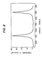
- the four-cycle and four-cylindered gasoline engine was actuated with the total load at 6,000 rpm and the measured voltage ⁇ V output from the semiconductor pressure transducer was recorded in an oscillograph.
- Fig. 8 shows the measured data, wherein the abscissa represents a crank angle and the ordinate represents the measured voltage ⁇ V output from the semiconductor pressure transducer of the present invention converted into the pressure P of the combustion gas with respect to the crank angle.
- the semiconductor pressure transducer of the present invention can accurately detect the pressure P of the combustion gas which is considered to be difficult to measure by a conventional pressure transducer, especially, by a pressure transducer using a semiconductor single crystal, namely, the pressure P of the combustion gas of an engine actuated at 6,000 rpm with the total load, the pressure changing with a change of the crank angle.
- the composite seat 81 and the supporting plate 40 are so formed as to make the heat transfer from the diaphragm 10 to the Si single crystal 70 difficult.
- the measured voltage ⁇ V was stably output from the Si single crystal 70 in the 100-hour continuous measurement of the pressure P of high-temperature and high-pressure fluid.
- the semiconductor pressure transducer of the present invention has high reliability as a device for measuring the pressure of high-temperature and high-pressure fluid.
- Fig. 9 shows another embodiment of a semiconductor pressure transducer according to the present invention.
- a first characteristic of this embodiment lies in a composite seat 82.
- the composite seat 82 includes a first seat portion 82a composed of crystallized glass 1 mm2 in area and 0.75 mm in height and a second seat portion 82b composed of a split steel sphere 1.5 mm in diameter.
- the first and second seat portions 82a and 82b are integrally provided through a high-temperature adhesive 82d.
- the first seat portion 82a of the thus-obtained composite seat 82 is electrostatically bonded to the crystal face 72 of the Si single crystal 70.
- a second characteristic of this embodiment is that a pressure transmitting portion 16 for accurately transmitting the pressure P applied to the diaphragm 10 to the composite seat 82 is provided at the center of the back surface of the diaphragm 10, and that the pressure transmitting portion 16 is composed of stabilized ZrO2 having a higher mechanical strength and not less high thermal conductivity than the crystallized glass which constitutes the first seat portion 82a.
- the pressure transmitting portion 16 is 1.7 mm2 in area and 2 mm in height.
- the semiconductor pressure transducer of this embodiment having the above-described structure enables accurate measurement of the pressure P of high-temperature and high-pressure fluid as the first embodiment.
- the second seat portion 82b is composed of the split steel sphere which is more excellent in mechanical strength than crystallized glass, the compression force W converted by the diaphragm 10 is constantly applied to the center of the composite seat 82, thereby enabling more accurate measurement of the pressure P applied to the surface of the diaphragm 10.
- the composite seat of the semiconductor pressure transducers is composed of two kinds of materials in the first and second embodiments, the number of kinds of the materials is not restricted to two and may be three or more as occasion demands.
- Si single crystal having a crystal face of (110) is used for the pressure detector in these embodiments, but an Si single crystal having a crystal face of ⁇ 110 ⁇ which is equivalent to the crystal face (110), as shown in Table 1, may be used for the pressure detector.
- Fig. 10 shows a first pressure detector 20.
- the first pressure detector 20 includes the Si single crystal 70 so formed as to have a crystal face of (110) as the surface to which a compression force is applied, the seat 80 bonded to the crystal face 72 of (110) of the Si single crystal 70 and transmitting the pressure P applied to the diaphragm 10 perpendicularly to the crystal face 72 as the compression force W, and the support base 90 bonded to the other crystal face 74 of the Si single crystal 70 and supporting the Si single crystal 70.
- the Si single crystal 70 is provided with the electrodes 76, 76′, 78 and 78′, as in the first and second embodiments.
- a current I is first applied to the Si single crystal 70 from the input electrodes 78, 78′ so that the voltage ⁇ V is taken out of the output electrodes 76, 76′, and in this state the compression force W is applied to the top surface 84 of the seat 80.
- the resistivity ⁇ , the current value I and the compression stress ⁇ Z of the Si single crystal 70 cannot be increased to a range exceeding common-sense for the following reasons.
- the resistivity ⁇ of the Si single crystal 70 exceeds 10 ⁇ cm, it is difficult to produce good electrical connection between a plurality of electrodes provided thereon.
- the resistivity ⁇ of the Si single crystal 70 at room temperature leaves the range of 10 ⁇ cm (corresponding to an impurity density of about 1 ⁇ 1015/cm3) to 1 ⁇ 10 ⁇ 4 ⁇ cm (corresponding to an impurity density of about 1 ⁇ 1021/cm3), the change in the measured voltage ⁇ V with a change in room temperature is disadvantageously greatly increased.
- the Si single crystal 70 constituting the pressure detector 20 of the present invention preferably has a resistivity ⁇ controlled in the range of 10 ⁇ cm to 1 ⁇ 10 ⁇ 4 ⁇ cm and, hence, the impurity density of the Si single crystal 70 is controlled in the range of 1 ⁇ 1015/cm3 to 1 ⁇ 1021/cm3.
- the piezoresistive coefficient ⁇ 63′ of the Si single crystal 70 depends on the resistivity ⁇ , the range of the piezoresistive coefficient ⁇ 63′ is also restricted for the same reason.
- the breaking strength of the Si single crystal 70 against a compression force is about 50 kg/mm2 (500 N/mm2) at maximum. It is therefore necessary to prevent the compression stress ⁇ Z exceeding the breaking strength of 50 kg/mn2 (500 N/mm2) from being applied to the Si single crystal 70. It is preferable to apply a compression stress of not more than 25 kg/mm2 (250 N/mm2).
- the current value I flowing in the Si single crystal 70 is not excessive. If an excess current I flows in the Si single crystal 70, the Si single crystal 70 itself releases much heat as an electric resistor, thereby exerting deleterious influence on the other characteristics not to mention of the measured voltage ⁇ V.
- the impurity density of the Si single crystal 70 is controlled in the range of 1 ⁇ 1015/cm3 to 1 ⁇ 1021/cm3.
- the compression stress ⁇ Z applied to the Si single crystal 70 does not exceed the limitation of the breaking strength of the Si single crystal 70. It has been confirmed from the experiments that a compression stress ⁇ Z not exceeding 50 kg/mm2 is allowable and a compression stress ⁇ Z not exceeding 25 kg/mm2 is preferable.
- the current I flowing in the Si single crystal 70 is set in the range which does not cause the Si single crystal 70 to release much heat. It has been confirmed from the experiments that the current I set in the range in which the consumption power does not exceed about 30 mW is preferable.
- the present inventors investigated the reduction in h in the formula (3), namely, the thickness h of the Si single crystal 70 in order to further increase the voltage ⁇ V output from the Si single crystal 70 while satisfying the above-described preferred conditions.
- the Si single crystal 70 is generally produced from an Si single crystal wafer having a diameter of not less than 1.5 inches (38 mm). As well known, the Si single crystal wafer is produced to a thickness of at least 200 ⁇ m for facilitating handling in various IC processings. A commercially available wafer 5 inches (127 mm) in diameter has a thickness of about 500 ⁇ m.
- a commercially available Si single crystal wafer having a crystal face of (110) is first cut out to form the Si single crystal 70.
- the crystal face 74 of (110) is bonded to the support base 90 and lined to facilitate handling.
- the other crystal face 72 of the Si single crystal 70 is ground by a chemical method together with a mechanical method to a thickness of not more than 50 ⁇ m, which is considered to be difficult to produce and put on the market as an ordinary Si single crystal.
- the output electrodes 76, 76′ and the input electrodes 78, 78′ are attached to the Si single crystal 70 and the seat 80 is bonded to the crystal face 72.
- the first pressure detector 20 is capable of producing the measured voltage ⁇ V which is sufficiently large for practical use while satisfying the preferred conditions for the Si single crystal 70 by reducing the thickness h of the Si single crystal 70 to not more than 50 ⁇ m.
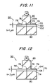
- Fig. 11 shows a second pressure detector 20.
- the second pressure detector 20 includes a semiconductor layer 102 so formed as to have a crystal face of (110) which is covered with an insulation film 100, and the Si single crystal 70 grown on the insulation film 100.
- the crystal face 72 of the Si single crystal 70 is bonded to the seat 80, and the semiconductor layer 102 is bonded to the support base 90.
- the impurity density of the Si single crystal 70 is also controlled in the range of 1 ⁇ 1015/cm3 to 1 ⁇ 1021/cm3 so as to reduce the influence of temperature on the voltage ⁇ V.
- the self sensitivity compensating method is applicable in two impurity density regions, namely, the regions of about 5 ⁇ 1018/cm3 and about 2 ⁇ 1020/cm3.
- the impurity densities in these regions are about 2 ⁇ 10 ⁇ 2 ⁇ cm and 6 ⁇ 10 ⁇ 4 ⁇ cm in terms of resistivity ⁇ of the p-conduction type Si single crystal 70. If it is assumed that the pressure transducer 20 shown in Fig.
- the Si single crystal 70 having a resistivity ⁇ of 6 ⁇ 10 ⁇ 4 ⁇ cm and a thickness of 200 ⁇ m, when the current I is applied to the Si single crystal 70 in the range in which the consumption power does not exceed 30 mW, and the compression force W of 50 kg/cm2 in terms of a compression stress ⁇ Z , which is the maximum compression stress allowable, is applied thereto, the measured voltage ⁇ V becomes as small as 3 mV or less, which is unsuitable for practical use.
- the thickness of the Si single crystal 70 in order to make the self sensitivity compensation method applicable and to obtain the measured voltage ⁇ V of not less than 10 mV, which is considered to be the lower limit for practical use, the thickness of the Si single crystal 70 must be not more than 1 ⁇ m.
- the second pressure detector is characterized in that it is provided with the self sensitivity compensation function disclosed in Japanese Patent Publication No. 58791/1982 by forming the Si single crystal 70 having a crystal face (110) and a very small thickness h as shown in Fig. 11 by the following IC process manufacturing technique.
- thermal diffusion, CVD, etc can be adopted as a means for forming an electrical insulation film 100 such as SiO2 and Si3N4 on the semiconductor layer 102.
- the Si single crystal 70 on the insulation film 100 As a means for forming the Si single crystal 70 on the insulation film 100, epitaxial growth and CVD are applicable. It is easy to form the Si single crystal 70 having a crystal face (110) and a thickness of not more than 20 ⁇ m by a combination of such at technique with a technique such as etching and laser recrystallization.
- the Si single crystal 70 is so formed as to have a self sensitivity compensation function by restricting the impurity density to about 5 ⁇ 1018/cm3 and about 2 ⁇ 1020/cm3 in which the deleterious influence of change of temperature on the characteristics is small.
- the second pressure detector 20 not only is provided with the self sensitivity compensation function but also can produce the measured voltage ⁇ V sufficiently large for practical use from the output electrodes 76, 76′.
- the Si single crystal 70 is provided on the electric insulation film 100 in the second pressure detector 20 in accordance with the present invention, there is no fear of electric leakage and since it is possible to have a comparatively high impurity density, the pressure transducer 20 can sufficiently withstand the use at a high temperature.
- a third pressure detector not only is provided with the self sensitivity compensation function but also can produce the measured voltage ⁇ V sufficiently large for practical use by forming the Si single crystal 70 having a crystal face (110) and having a small thickness by using the IC process manufacturing technique.
- Fig. 12 shows a third pressure detector 20 of the present invention.
- the Si single crystal 70 includes a conduction layer 104 in which the impurity density is controlled in the range of 1 ⁇ 1015/cm3 to 5 ⁇ 1021/cm3 and an insulation layer 106 provided adjacent to the conduction layer 104.
- the insulation layer 106 is bonded to the support base 90 and the conduction layer 104 is bonded to the seat 80.
- a pair of output electrodes 76, 76′ and a pair of input electrodes 78, 78′ provided on the Si single crystal 70 are electrically connected with at least the conduction layer 104, that in the conduction layer 104 the impurity density is controlled in the range of 1 ⁇ 1015/cm3 to 1 ⁇ 1021/cm3, and that the thickness h of the Si single crystal 70 is made small so as to take a large output voltage ⁇ V.
- the conduction layer 104 is formed on the insulation layer 106 by thermal diffusion or ion implantation.
- resistor layer isolation As a technique for electrically insulating the conduction layer 104 from the insulation layer 106, p-n junction isolation or what is called resistor layer isolation utilizing a difference in the resistance can be used.
- resistor layer isolation the resistance of the passage of the conduction layer 104 in which a current flows is regulated to not more than 1/100 of the resistance of the passage of the insulation layer 106 in which a current flows in order to maintain the accuracy of 1%.
- the third pressure transducer 20 not only is provided with the self sensitivity compensation function but also can produce a sufficiently large measured voltage ⁇ V from the output electrodes 76, 76′ in the same way as in the second pressure transducer 20.
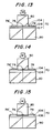
- Fig. 13 shows a modification of the third pressure transducer 20.
- the Si single crystal 70 includes the conduction layer 104 in which the impurity density is controlled in the range of 1 ⁇ 1015/cm3 to 1 ⁇ 1021/cm3 in order to detect the compression force applied thereto and the insulation layer 106 provided adjacent to the conduction layer 104 in order to be electrically insulated from the conduction layer 104.
- the conduction layer 104 and the insulation layer 106 are formed on the crystal face side of an Si single crystal layer 107 of 200 ⁇ m thick by impurity diffusion.
- Fig. 14 shows another modification of the third pressure transducer 20.
- This pressure transducer is characterized in that the conduction layer 104 is so provided as not to protrude from the side surface of the Si single crystal 70.
- This structure also enables a sufficiently large measured voltage ⁇ V to be taken out in the same way as in the third pressure transducer 20 without much influence of change of temperature on the characteristics.
- Fig. 15 shows still another modification of the third pressure transducer 20.
- This pressure transducer is characterized in that the conduction layer 104 is formed on the Si single crystal 70 having a crystal face (110) by ion implantation, thereby producing the same effect as the third pressure transducer 20.
- Si single crystal having a crystal face of (110) is used for these pressure detectors, but an Si single crystal having a crystal face of ⁇ 110 ⁇ which is equivalent to the crystal face (110), as shown in Table 1, may be used instead.
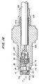
- Fig. 16 shows a pressure sensor for high-temperature fluid of this embodiment.
- the same reference numerals are provided for the elements which are the same as those in the first and second embodiments, and explanation thereof will be omitted.
- the pressure sensor is composed of a substantially cylindrical sensor case 110 and the diaphragm attached to the opening of the sensor case 110.
- the pressure P acts on the Si single crystal 70 through a pressure transmitting portion 18 composed of a thermally insulating material and the seat 80 as the compression force, whereby the measured voltage corresponding to the pressure P is output from the Si single crystal 70 through a lead wire 132.
- the surface 12 of the diaphragm 10 is exposed to the high-temperature and high-pressure fluid.
- a material having a good thermal conductivity is used for the sensor case 110. It is further preferable that the heat is released from a groove 126 for a fixing screw of the sensor case 110 to a cylinder head portion (not shown).
- the pressure sensor of this embodiment uses the first pressure detector as the pressure detector 20.
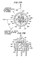
- the pressure detector 20 has a stem 140 shown in Fig. 17.
- the stem 140 includes the support base 90 which is bonded to the other crystal face 74 of the Si single crystal 70 for supporting the Si single crystal 70, a plurality of input electrode terminals 144, 144′ for applying a current from the outside to the input electrodes 78, 78′, a plurality of output electrode terminals 142, 142′ for taking the electric signals output from output electrodes 76, 76′ to the outside, and holding means for integrally holding these electrode terminals 142, 142′, 144 and 144′ and the support base 90.
- these electrode terminals 142, 142′, 144 and 144′ are annually disposed around the support base 90 in such a manner as to be substantially symmetrical to each other.
- the stem 140 uses a substantially cylindrical ring 148 and sealing glass 146 as the holding means. Into the ring 148 with the upper end open, the support base 90 and the electrode terminals 142, 142′, 144 and 144′ are inserted and integrally fixed thereat by using the sealing glass 146.
- each of the electrode terminals 142, 142′, 144 and 144′ is substantially flush with the crystal face 72 of the Si single crystal 70 and is connected to the corresponding electrodes 76, 76′, 78, 78′ through a gold wire 130.
- the other ends of the electrode terminals 142, 142′, 144 and 144′ are led to the outside through through holes 150 provided on the bottom surface of the ring 148 and are connected to the lead wire 132 shown in Fig. 16 so as to be electrically connected to an external measuring instrument through the lead wire 132.
- the output electrode terminals 142, 142′ and the input electrode terminals 144, 144′ are integrally provided with the support base 90 as the stem 140. Accordingly, electrical connection is completed merely by connecting the electrodes 76, 76′, 78 and 78′ of the Si single crystal 70 bonded to the support base 90 with the electrode terminals 142, 142′, 144 and 144′, respectively, through the short lead wires 130 of, e.g., 10 mm long, thereby facilitating electrical connection.
- the ring and the sealing glass are used as the holding means, but they may be replaced by another means so long as it can integrally hold the electrode terminals 142, 142′, 144 and 144′ and the support base 90.
- a ceramic package may be used.
- this embodiment adopts a novel pressure detecting system in which the pressure of high-temperature fluid acting on the surface of the diaphragm is applied perpendicularly to the crystal face ⁇ 110 ⁇ of the Si single crystal as the compression force through the seat which serves as the transmitting means.
- the electric connection of the Si single crystal is facilitated by short conductors without leading around lead wires by providing a stem for integrally holding the support base which supports the Si single crystal and the input and output electrode terminals connected to the corresponding input and output electrodes of the Si single crystal by using a holding means. Consequently, it is possible to produce an inexpensive and highly reliable pressure sensor which is easily produced and is scarcely influenced by noise.
- This pressure sensor is produced by inserting the flange portion 11a of the diaphragm 10 into the opening portion of the substantially cylindrical sensor case 110 and the fitted portions are bonded by projection welding over the entire periphery so as to prevent the combustion gas from entering the interior of the sensor case 110.
- a block portion 120 is provided at the central portion of the surface of the diaphragm 10 so as to absorb the heat of the combustion gas in the vicinity of the diaphragm 10 and the heat transferred to the diaphragm 10 itself.
- the temperature of the block portion 120 must be lower than the temperature of the diaphragm 10.
- the block portion 120 is therefore be required to have a large specific heat and a large thermal conductivity. If the block portion 120 is too large, the number of natural oscillation of the diaphragm 10 is unfavorably lowered.
- the pressure sensor in accordance with the present invention when used as a combustion pressure sensor, if the weight of the block portion 120 is increased and, hence, the intrinsic number of natural oscillation of the diaphragm is lowered, the measurable range of number of vibration is reduced, so that when the combustion pressure sensor is attached to a vigorously vibrating element such as an engine, it is difficult to detect a signal indicating knocking or the like.
- the block portion 120 is therefore required to reduce the specific weight with respect to the diaphragm 10, and with the reduction in the specific weight, the detecting characteristic of the sensor is enhanced.
- the diaphragm 10 and the block portion 120 are provided separately from each other.
- a protrusion 10a provided in the vicinity of the central portion of the surface of a thin plate portion 11b of the diaphragm 10 is engaged with a recessed portion 120a provided at the central portion of the block portion 120, whereby the block portion 120 is secured to the central portion of the diaphragm 10.
- This structure allows the diaphragm 10 and the block portion 120 to be produced from different materials. That is, it is possible to use a material having an excellent spring characteristic at a high temperature, e.g., SUS 430, and Inconel X720 for the diaphragm 10 and a material having a good thermal conductivity, e.g., an Al alloy for the block portion 120.
- a material having an excellent spring characteristic at a high temperature e.g., SUS 430, and Inconel X720 for the diaphragm 10
- a material having a good thermal conductivity e.g., an Al alloy for the block portion 120.
- the block portion 120 is made of an Al alloy, the mass becomes about 1/3 in comparison with a conventional block portion made of an Fe or Ni alloy.
- an Al alloy is used for the block portion 120, it is possible to triple the heat capacity without substantially any change in the responsiveness and the acceleration sensitivity by tripling the volume of a conventional block portion.
- the block portion 120 is made of an Al alloy, the specific heat becomes about 2 times and the thermal conductivity about 3 times in comparison with a conventional block portion made of an Fe or Ni alloy.
- the block portion 120 of this embodiment it is possible to increase the specific heat of the block portion to about 2 times and the thermal conductivity thereof to about 3 times and to reduce the specific weight to about 1/3 in comparison with a conventional block portion by forming the diaphragm 10 from a material having an excellent spring characteristic at a high temperature such as SUS 430, and Inconel X720 and the block portion 120 from, for example, an Al alloy.
- a material having an excellent spring characteristic at a high temperature such as SUS 430, and Inconel X720 and the block portion 120 from, for example, an Al alloy.
- the protrusion 10a is so designed as not to be enlarged toward the end and the recessed portion 120a is so designed that the inner wall is in conformity with the protrusion 10a and is not enlarged toward the bottom. In this way, the production of the block portion 120 and the diaphragm 10 is facilitated by press molding, thereby enhancing the mass productivity of the pressure sensor and reducing the manufacturing cost.
- the block portion 120 When the block portion 120 is bonded to the surface of the diaphragm 10, substantially the entire surface of the diaphragm 10 is covered with the block portion 120 through a gap 122 as if by an umbrella.
- the size of the gap 122 can be controlled as desired by the dimensions of the protrusion 10a and the recessed portion 120a. In Fig. 16, the gap is substantially zero. In this way, the block portion 120 can absorb the heat of the combustion gas in the vicinity of the diaphragm immediately after it is generated.
- the amount of heat transferred directly from the combustion gas to the diaphragm 10 is therefore greatly reduced and, as s result, the rise in the temperature of the diaphragm 10 is effectively suppressed and the creep and the like of the diaphragm can be reduced.
- the outer periphery of the pressure detector 20 is attached to the internal peripheral surface of the sensor case 110 through the stem 140.
- the electrode terminals 142, 142′, 144 and 144′ are provided in the stem 140, as shown in detail in Fig. 17, and one end of each of these electrode terminals is electrically connected to the corresponding input or output electrode through the Au wire 130. The other end of each of these electrode terminals is connected to the lead wire 132, which is lead to the outside of the sensor case 110.
- a caulking portion 110a for lead wire is provided at the other end of the pressure sensor in order to prevent the lead wire 132 from slipping off and to prevent the tensile strength applied to the lead wire 132 from being applied to the electrode terminals 142, 142′, 144 and 144′.
- the caulking portion 110a of the sensor case 110 is covered with a case cover 124.
- the groove 126 for a fixing screw is provided on the outer peripheral portion of the sensor case 110 at the one end on the diaphragm side, and the sensor case 110 is easily attached to the desired position by engaging the groove 126 with a groove provided on the inner peripheral portion of a predetermined mounting hole (not shown).
- Fig. 17 shows the details of the pressure detector 20 used for the pressure sensor.
- the Si single crystal 70 is a p-type Si single crystal having an impurity density of 1 ⁇ 1016/cm3 which is in the range of 1 ⁇ 1015/cm3 to 1 ⁇ 1021/crs3 (a resistivity ⁇ of about 1 ⁇ cm), an area of 1.7 mm2 and a thickness of 17 ⁇ m.
- a pair of opposing output electrodes 76, 76′ having a width of 0.1 mm are provided on the crystal face 72 of the Si single crystal 70 in the direction having an angle of 45 degrees with the direction of ⁇ 001> by the deposition of aluminum, as shown in Fig. 17(A).
- a pair of opposing input electrodes 78, 78′ having a width of 0.9 mm are provided in the direction having an angle of 45 degrees with the direction of ⁇ 1 1 0> by the deposition of aluminum.
- the seat 80 is composed of crystallized glass 1 mm2 in area and 1.1 mm in height.
- the support base 90 is composed of crystallized glass having a thermal expansion coefficient approximate to that of the Si single crystal 70 and so formed as to have an area of 1.7 mm2 and a height of 3 mm.
- the ring 148 is formed into a substantially cylindrical shape with one end open by using an Fe-Ni-Co alloy, and provided at the bottom portion with a plurality of through holes 150 for inserting electrode terminal therethrough.
- Each of the electrode terminals 142, 142′, 144 and 144′ is formed into a narrow and long rod shape having a diameter of 0.5 mm, and is inserted into the stem 140 to be fixed thereto with one end a thereof being substantially flush with the crystal face 72 of the Si single crystal 70.
- a gold plated layer is provided on the one end a of each of the input electrode terminals 144, 144′ and is connected to the corresponding input electrodes 78, 78′ through the gold wire 130 having a diameter of 0.05 mm.
- a gold plated layer is provided on the one end a of each of the output electrode terminals 142, 142′ and is connected to the corresponding output electrodes 76, 76′ through the gold wire 130 having a diameter of 0.05 mm.
- the current I was applied to the Si single crystal 70 in the range in which the consumption power did not exceed 30 mW and a compression force of 5 kg (50 N) applied to the Si single crystal 70 through the seat 80 so that the compression stress ⁇ Z is 15 kg/mm2 (150 N/mm2), which is within the range of breaking strength that does not break the Si single crystal 70.
- the resistance between the pair of input electrodes provided on the Si single crystal 70 what is called input resistance was 800 ⁇ at room temperature. Therefore, a current I of 6 mA was applied from the input electrodes 78, 78′ to the Si single crystal 70 so that the consumption power did not exceed 30 mW.
- a voltage ⁇ V of about 110 mV was obtained at room temperature from the output electrodes 76, 76′ of the Si single crystal 70.
- the rate of change in the measured voltage ⁇ V in the range of -40 to 150°C was 0.15%/°C. It was therefore confirmed that the pressure detector 20 of this embodiment can output a voltage ⁇ V sufficiently large for practical use and that the influence of change of temperature on the characteristics was very small.
- the conduction type is not restricted to the p-type and the same effect is obtained by using an n-conduction type Si single crystal 70.
- the pressure detector 20 of this embodiment it is possible to obtain a large measured voltage ⁇ V by reducing the thickness h of the Si single crystal 70. This effect becomes more prominent as the impurity density is increased toward 1 ⁇ 1021/cm3.
- the side of the seat 80 to which the compression force W is applied has a flat shape.
- a convex or concave surface may be provided in a part or over the entire surface on the side to which the compression force W is applied so that the compression force W applied from the pressing surface of the pressing plate acts substantially on the center of the seat 80.
- the compression force W may be applied to the outwardly curved surface 81 of the seat 80.
- the pressure transmitting portion 18 composed of a thermally insulating material is used in order to prevent the heat transfer from the diaphragm 10 to which the pressure P is applied to the Si single crystal 70 in this embodiment, pressure can be measured without using the thermally insulating material by forming the seat 80 into a composite seat excellent in thermal insulating property.
- the seat 80 is preferably composed of a material having a thermal expansion coefficient which is approximate to that of the Si single crystal 70.
- the other end of the seat 80 is in contact with the diaphragm 10.
- This portion of the seat is preferably made of a material having an excellent mechanical strength or thermal insulation property.
- the portion of the seat 80 which is to be bonded to the Si single crystal 70 is preferably made of an electrically insulating material having a thermal expansion coefficient which is approximate to that of the Si single crystal 70 and the portion which is to be brought into contact with the diaphragm 10 is preferably made of a material more excellent in mechanical strength or thermal insulation property than the material for the bonding portion with the Si single crystal 70.
- the seat 80 By forming the seat 80 itself as a composite seat consisting of a combination of two kinds of materials, as described above, in the case of measuring the pressure of high-temperature and high-pressure fluid such as combustion gas in the cylinder of an internal combustion engine, the heat transmitted to the diaphragm is alleviated by the seat 80 and does not act on the Si single crystal 70 as a high temperature.
- the Si single crystal 70 is therefore capable of outputting the voltage corresponding to the pressure P applied to the diaphragm 10 without being influenced by the ambient temperature.
- a compression force sometimes locally acts on the diaphragm 10 due to local contact according to the state of the bonded area.
- the seat 80 is sometimes plastically deformed or broken.
- the seat 80 is not broken due to the local contact of the portion of the seat 80 bonded to the diaphragm 10, thereby enabling accurate measurement of the pressure P.
- the pressure sensor for high-temperature fluid can use the second pressure detector shown in Fig. 11 or the third pressure detector shown in Fig. 12 in place of the first pressure detector.
- the second pressure detector 20 includes the Si semiconductor layer 102 so formed as to have a crystal face of (110) and having an area of 1.7 mm2 and a thickness of 200 ⁇ m, the SiO2 electrical insulation film 100 of 1 ⁇ m thick formed by heat treating the side surface side of the semiconductor layer 102 at a high temperature, and the Si single crystal 70 having a crystal face of (110) grown on the insulation film 100 to a thickness h of 1 ⁇ m by epitaxial growth.
- the crystal face 72 of the Si single crystal 70 is bonded to the seat 80 by electrostatic bonding, and the support base 90 is bonded to opposite side of the semiconductor layer 102 relative to the insulation film 100 by electrostatic bonding.
- the Si single crystal 70 is a p-conduction type Si single crystal which contains thermally diffused boron at a density of 1 ⁇ 1019/cm3 (resistivity ⁇ of about 0.01 ⁇ cm), which is in the range of 1 ⁇ 1015/cm3 to 1 ⁇ 1021/cm3.
- the series of steps of forming the insulation film 100 on the semiconductor layer 102, and adjusting the impurity density of the Si single crystal 70 to 1 ⁇ 103 in accordance with IC manufacturing process technique are actually carried out in the wafer manufacturing stage. Thereafter, the wafer is cut by a dicer into an area of 1.7 ⁇ 1.7 mm2, as shown in Fig. 7.
- the current I was applied to the Si single crystal 70 of the thus-produced pressure detector in the range in which the consumption power did not exceed 30 mW at room temperature and a compression force of 15 kgw (150 N) was also applied thereto in order to confirm the effect of reducing the thickness of the Si single crystal 70 and prove that the influence of change of temperature on the characteristics is small, in the same way as in the first example.
- the pressure detector 20 in this example can output a voltage ⁇ V sufficiently large for practical use and that the influence of change of temperature on the characteristics was very small.
- the pressure detector 20 in this example since the Si single crystal 70 is provided on the main surface 100a of the electrical insulation film 100, there is no current leakage even at a high temperature. Thus, the pressure detector is highly reliable.
- the conduction type is not restricted to the p-type and the same effect is obtained by using an n-conduction type Si single crystal 70.
- the Si single crystal 70 having a crystal face (110) is formed by epitaxial growth, the method is not restricted thereto and the Si single crystal 70 may be formed by using CVD or MBE growth together with a laser recrystallization technique.
- the Si single crystal 70 is a p-conduction type Si single crystal 70 so formed as to have a crystal face of (110) and a thickness h of 200 ⁇ m.
- the Si single crystal 70 includes the p-conduction type conduction layer 104 for sensing compression force which has a thickness h of 2 ⁇ m and in which boron is thermally diffused at an impurity density of 5 ⁇ 1018/cm3 (resistivity ⁇ of about 2 ⁇ 10 ⁇ 2 ⁇ cm), and the insulation layer 106 for electrically insulating the conduction layer 104 so that the conduction layer 104 functions at an accuracy of at least 1%.
- the impurity density of the Si single crystal 70 is so controlled that the resistance of the passage of the conduction layer 104 in which a current flows from the input electrode 78 toward the opposite input electrode 78′ is regulated to not more than 1/100 of the resistance of the passage of the insulation layer 106 in which a current flows in the same way.
- the seat 80 is electrostatically bonded to the one crystal face 72 of the Si single crystal 70 and the support base 90 is electrostatically bonded to the other crystal face 74.
- the input electrodes 78, 78′ and the output electrodes 76, 76′ are formed by deposition so as to be electrically connected to at least the conduction layer 104, thereby taking the measured voltage ⁇ V based on the piezoresistive effect of the conduction layer 104.
- the current I was applied to the Si single crystal 70 of the thus-produced pressure detector 20 in the range in which the consumption power did not exceed 30 mW at room temperature in order to confirm the effect of reducing the thickness of the Si single crystal 70 and prove that the influence of change of temperature on the characteristics is small, in the same way as in the first and second examples.
- the Si single crystal 70 which serves both as the conduction layer 104 and the electrical insulation layer 106 is formed into a p-conduction type by using resistor layer isolation in this example, it is also possible to produce a pressure detector having substantially the same effect by forming an n-conduction type Si single crystal 70 by using resistor layer isolation.
- the conduction layer 104 may be either of a p-conduction type or an n-conduction type.
- the conduction layer 104 and the electric insulation layer 106 are formed by p-n junction isolation.
- the output electrodes 76, 76′ and the input electrodes 78, 78′ must be electrically connected only to the conduction layer 104 and the electrical isolation function is substantially restricted to a temperature range of about 150°C.
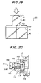
- Fig. 19 shows a pressure sensor of this embodiment.
- the same reference numerals are provided for the elements which are the same as those in the third embodiment, and explanation thereof will be omitted.
- This embodiment is characterized in that a threaded hole 160 is provided on the surface of the thin plate portion 11b of the diaphragm 10 in the direction of application of pressure, and an adjust screw 162 is engaged with the threaded hole 160 so as to deform the thin plate portion 11b in the direction of application of pressure, thereby applying a desired preload to the pressure detector 20.
- the threaded hole 160 is provided from the block portion 120 toward the central portion of the thin plate portion 11b.
- the adjust screw 162 is composed of a head portion 164 provided with a groove 164a which engages the tip of a driver and a screw portion 166 which engages the threaded hole 160.
- the tip of the screw portion 166 is formed into a cone shape so that the central portion of the tip effectively presses the center 11c of the surface of the thin plate portion 11b, thereby deforming the thin plate portion 11b.
- the diaphragm 10 is so formed that the thin plate portion 11b is deformed in the right direction seen in Fig. 19 by the pressing force of the adjust screw 162. It is also necessary that the threaded hole 160 is so formed as not to penetrate to the back side of the thin plate portion 11b.
- the adjust screw 162 is first tightened while measuring the output of the pressure detector 20, whereby the tip of the adjust screw 162 is pressed against the center 11c of the thin plate portion 11b of the diaphragm 10.
- the center 11c of the thin plate portion 11b is deformed in the right direction seen in Fig. 19, and a preload is applied to the pressure detector 20 through the pressure transmitting portion 18 made of a thermally insulating material.
- an electric signal corresponding to the preload is output from the pressure detector 20 and the adjuster sets the preload value as follows while seeing the electric signal.
- Each part of a pressure sensor generally has a predetermined dimensional error, and an assembly error is produced in assembling each part.
- the diaphragm 10 is deformed by the amount corresponding to the height (about 0.2 mm) of the projection of the weld. Therefore, if the diaphragm 10 is brought into contact with the pressure sensor 20 secured to the sensor case 110 during the welding for assembling the pressure sensor, the impact force is applied to the pressure sensor 20, thereby involving the danger of breaking the pressure sensor 20. It is therefore desirable to gently apply a preload to the pressure detector 20 after the assembly, in particular, after the projection welding of the diaphragm 10 and the sensor case 110.
- the preload value at the value of not less than a predetermined lower limit so as to prevent the expansion or contraction of the diaphragm 10 and the sensor case 110 due to heat from obstructing the application of a pressure from the diaphragm 10 to the pressure detector 20 and to enable the accurate detection of the negative load and the like acting on the surface of the diaphragm 10.
- the preload value is set at a value of not more than a predetermined upper limit so as not to produce a fatigue failure on the pressure detector 20 when a pressure is measured repeatedly by using the pressure sensor.
- the preload value is adjusted so as to exist between the lower limit and the upper limit by adjusting the adjust screw 162.
- the adjust screw 162 is cut away at the position indicated by the broken line A - A′, thereby reducing the additive mass of the diaphragm 10 and enhance the resistance to vibration.
- the adjust screw 162 is engaged with the threaded hole 160 provided in the diaphragm 10. Therefore, when the mass of the adjust screw 162 is increased, the number of natural oscillation of the diaphragm 10 and, hence, the resistance to vibration is lowered, so that when the combustion pressure sensor is attached to a vigorously vibrating element such as an engine, the accuracy of detecting pressure is greatly lowered. To prevent this, in this embodiment, when preloading by the adjust screw 162 has been finished, the head portion 164 of the adjust screw 162 is cut away, thereby preventing the resistance to vibration of the combustion pressure sensor from lowering.
- the preload is adjusted by tightening the adjust screw 162 while seeing the measured value output from the Si single crystal 70.
- the adjust screw 162 may be provided with a narrow portion 165 having a predetermined screw breaking strength, as shown in Fig. 20.
- the head portion 164 is cut away from the narrow portion 165 at the point at which the tightening force has exceeded the screw breaking strength, whereby the preload applied from the screw portion 166 to the Si single crystal 70 is adjusted to a constant value.
- Si single crystal having a crystal face of (110) is used for the pressure detector in these embodiments, but an Si single crystal having a crystal face of ⁇ 110 ⁇ which is equivalent to the crystal face (110), as shown in Table 1, may be used for the pressure detector.
- a method of producing a pressure detector used in the present invention will now be explained with reference to a method of producing the pressure detector shown in Fig. 4.
- the Si single crystal 70 is formed as a p-type Si single crystal having a resistivity of 10 ⁇ cm, an area of 1.7 mm2 and a thickness of 0.2 mm.
- a pair of opposing output electrodes 76, 76′ are provided on the one crystal face 72 of the Si single crystal 70 in the direction having an angle of 45 degrees with the direction of [001] by the deposition of aluminum, and a pair of opposing input electrodes 78, 78′ are provided in the direction having an angle of 45 degrees with the direction of [1 1 0] by the deposition of aluminum.
- the support base 90 is composed of crystallized glass having a thermal expansion coefficient approximate to that of the Si single crystal 70 and having an area of 1.7 mm2 and a thickness of 1 mm.
- the seat 80 is composed of cubic crystallized glass 1 mm2 in area and 1 mm in thickness.
- Fig. 21 shows a preferred embodiment of a method of producing the pressure detector 20.
- an Si single crystal wafer 200 is so formed as to have a crystal face (110) as the surface to which the compression force is applied.
- the output electrodes 76, 76′ and the input electrodes 78, 78′ are provided on the one crystal face 72 of the Si single crystal wafer 200 by the deposition of aluminum in accordance with a predetermined pattern, as shown in Fig. 22.
- a plurality of seats 80 are provided in such a manner as to be surrounded by matrix grooves 240 of a predetermined pattern.
- the width of the matrix groove 240 is set at w2.
- the seat wafer 230 is positioned on the crystal face 72 of the Si single crystal wafer 200 by a positioning jig (not shown) and electrostatically bonded with the Si single crystal wafer 200.
- Fig. 22 shows the seat wafer 230 positioned on the crystal face 72 of the Si single crystal wafer 200.
- the seats 80 surrounded by the matrix grooves 240 are only shown.
- plural pairs of output electrodes 76, 76′ and input electrodes 78, 78′ are provided on the crystal face 72 of the Si single crystal wafer 200 in accordance with a predetermined pattern.
- the seat wafer 230 is positioned on the crystal face 72 of the Si single crystal wafer 200 such that each seat 80 is located at the center of the corresponding electrodes 76, 76′, 78, 78′ and electrostatically bonded with the Si single crystal wafer 200.
- the seat wafer 230 is diced along the matrix grooves 240 at a width of w1 and a seal holding portion 250 for the seats 80 is removed, as shown in Fig. 21.
- a plurality of seat wafers 230 are electrostatically bonded in matrix to the crystal face 72 of the Si single crystal wafer 200.
- the electrostatically bonded Si single crystal wafer 200 and the support base wafer 210 are diced along the centers 260 of the dicing grooves (matrix grooves 240), thereby cutting out a plurality of pressure detectors 20.
- the pressure detectors 20 are produced by a simple process comprising the steps of positioning the three wafers 200, 210 and 230 with each other, electrostatically bonding them, dicing the seat wafer 230 along the matrix grooves 240, and dicing the Si single crystal wafer 200 and the support base wafer 210 along the dicing grooves.
- the present invention since it is possible to position the parts 70, 80 and 90 in each wafer, accurate positioning is realized, thereby enabling the production of a pressure detector excellent in electric characteristics. Especially, according to this embodiment, it is possible to produce pressure detectors having uniform electric characteristics in the unit of a lot. Thus, the method of the present invention is suitable for mass-producing small devices such as pressure detectors.
- the manufacturing method of the pressure detector is not restricted to this embodiment, but various modifications are possible.
- the Si single crystal 70 and the seat 80 are electrostatically bonded directly with each other and the Si single crystal 70 and the support base 90 are also electrostatically bonded directly with each other, but various laminates may be provided on the bonded surfaces, if necessary.
- an Si single crystal wafer having a crystal face of (110) is used, but the present invention is not restricted thereto and an Si single crystal wafer having a crystal face equivalent to the crystal face (110), such as (1 1 0), ( 1 10) and ( 11 0), may be used instead.
- Si single crystal having a crystal face of (110) is used for these pressure detectors, but an Si single crystal having a crystal face of ⁇ 110 ⁇ which is equivalent to the crystal face (110), as shown in Table 1, may be used instead.
Applications Claiming Priority (14)
| Application Number | Priority Date | Filing Date | Title |
|---|---|---|---|
| JP186329/88 | 1988-07-26 | ||
| JP18633288A JPH0714071B2 (ja) | 1988-07-26 | 1988-07-26 | 力変換装置 |
| JP18632988A JPH0714069B2 (ja) | 1988-07-26 | 1988-07-26 | 力変換素子の製造方法 |
| JP9893388U JPH0526515Y2 (fr) | 1988-07-26 | 1988-07-26 | |
| JP1988098934U JPH0619068Y2 (ja) | 1988-07-26 | 1988-07-26 | 高温流体用の圧力センサ |
| JP186333/88 | 1988-07-26 | ||
| JP18633388A JPH0610641B2 (ja) | 1988-07-26 | 1988-07-26 | 高温流体用圧力センサ |
| JP98933/88U | 1988-07-26 | ||
| JP63186331A JPH0654274B2 (ja) | 1988-07-26 | 1988-07-26 | 半導体圧力変換器 |
| JP18633088A JPH0714070B2 (ja) | 1988-07-26 | 1988-07-26 | 力変換素子 |
| JP186331/88 | 1988-07-26 | ||
| JP98934/88U | 1988-07-26 | ||
| JP186330/88 | 1988-07-26 | ||
| JP186332/88 | 1988-07-26 |
Publications (3)
| Publication Number | Publication Date |
|---|---|
| EP0352773A2 true EP0352773A2 (fr) | 1990-01-31 |
| EP0352773A3 EP0352773A3 (fr) | 1991-04-03 |
| EP0352773B1 EP0352773B1 (fr) | 1993-04-14 |
Family
ID=27565619
Family Applications (1)
| Application Number | Title | Priority Date | Filing Date |
|---|---|---|---|
| EP89113807A Expired - Lifetime EP0352773B1 (fr) | 1988-07-26 | 1989-07-26 | Capteur de pression Si monocrystallin piezoresistif |
Country Status (3)
| Country | Link |
|---|---|
| US (1) | US4993266A (fr) |
| EP (1) | EP0352773B1 (fr) |
| DE (1) | DE68905967T2 (fr) |
Cited By (10)
| Publication number | Priority date | Publication date | Assignee | Title |
|---|---|---|---|---|
| EP0579226A2 (fr) * | 1992-07-16 | 1994-01-19 | Kabushiki Kaisha Toyota Chuo Kenkyusho | Transducteur de force et circuit de détection de pression utilisant celui-ci |
| EP0526600B1 (fr) * | 1991-02-27 | 1994-07-27 | Robert Bosch Gmbh | Capteur de pression pour la mesure de pression dans la chambre d'explosion d'un moteur a combustion interne |
| EP0493542B1 (fr) * | 1990-07-18 | 1995-08-30 | Robert Bosch Gmbh | Capteur de pression pour la determination de la pression dans la chambre de combustion d'un moteur a combustion interne |
| EP0735352A2 (fr) * | 1995-03-31 | 1996-10-02 | Kabushiki Kaisha Toyota Chuo Kenkyusho | Transducteur de force et son procédé de fabrication |
| EP1391709A2 (fr) * | 2002-08-23 | 2004-02-25 | Robert Bosch Gmbh | Dispositif de mesure d'une force, dispositif de mesure d'une pression et capteur de pression |
| WO2005001408A3 (fr) * | 2003-06-19 | 2005-03-24 | Dynisco Instr Inc | Transducteur de pression |
| FR2865275A1 (fr) * | 2003-12-25 | 2005-07-22 | Denso Corp | Element d'acquisition de grandeur physique ayant une structure amelioree convenant pour une liaison electrique et son procede de fabrication |
| FR2865803A1 (fr) * | 2004-02-03 | 2005-08-05 | Denso Corp | Capteur de pression comportant un diaphragme |
| DE102009039827A1 (de) | 2008-09-11 | 2010-04-15 | Piezocryst Advanced Sensorics Gmbh | Piezoelektrischer Drucksensor |
| US9851272B2 (en) | 2015-02-06 | 2017-12-26 | Viatran Corporation | Pressure sensor diaphragm |
Families Citing this family (30)
| Publication number | Priority date | Publication date | Assignee | Title |
|---|---|---|---|---|
| DE3811311C1 (fr) * | 1988-04-02 | 1989-03-09 | Robert Bosch Gmbh, 7000 Stuttgart, De | |
| US5182233A (en) * | 1989-08-02 | 1993-01-26 | Kabushiki Kaisha Toshiba | Compound semiconductor pellet, and method for dicing compound semiconductor wafer |
| DE4103704A1 (de) * | 1990-07-18 | 1992-01-23 | Bosch Gmbh Robert | Druckgeber zur druckerfassung im brennraum von brennkraftmaschinen |
| DE4103705A1 (de) * | 1990-07-18 | 1992-01-23 | Bosch Gmbh Robert | Druckgeber zur druckerfassung im brennraum von brennkraftmaschinen |
| US5606117A (en) * | 1991-02-27 | 1997-02-25 | Robert Bosch Gmbh | Pressure sensor for measuring pressure in an internal combustion engine |
| US5969591A (en) * | 1991-03-28 | 1999-10-19 | The Foxboro Company | Single-sided differential pressure sensor |
| DE4137624A1 (de) * | 1991-11-15 | 1993-05-19 | Bosch Gmbh Robert | Silizium-chip zur verwendung in einem kraftsensor |
| JP2553199Y2 (ja) * | 1991-12-26 | 1997-11-05 | 株式会社豊田中央研究所 | 力変換素子 |
| JPH0719981A (ja) * | 1993-06-01 | 1995-01-20 | Nippondenso Co Ltd | 高温用圧力センサ |
| FR2717262B1 (fr) * | 1994-03-14 | 1997-09-26 | Nippon Denso Co | Détecteur de pression. |
| JPH08178778A (ja) * | 1994-12-27 | 1996-07-12 | Mitsubishi Electric Corp | 半導体圧力検出装置 |
| JPH1038789A (ja) * | 1996-05-22 | 1998-02-13 | Ngk Insulators Ltd | 流体センサ |
| JPH11304612A (ja) * | 1998-04-24 | 1999-11-05 | Mitsubishi Electric Corp | 半導体圧力検出装置 |
| JP3407192B2 (ja) * | 1998-12-31 | 2003-05-19 | 株式会社ダイトー | テストハンドの制御方法及び計測制御システム |
| US6690284B2 (en) * | 1998-12-31 | 2004-02-10 | Daito Corporation | Method of controlling IC handler and control system using the same |
| JP2002310827A (ja) * | 2001-04-11 | 2002-10-23 | Denso Corp | 圧力センサ |
| US6634113B1 (en) * | 2002-05-17 | 2003-10-21 | Delphi Technologies, Inc. | Tilt sensor and method of forming such device |
| US7021154B2 (en) * | 2002-09-24 | 2006-04-04 | Kabushiki Kaisha Toyota Chuo Kenkyusho | Force sensing element |
| CN1247974C (zh) * | 2003-02-17 | 2006-03-29 | 株式会社电装 | 具有其中包含压力敏感元件的细长外壳的压力探测器 |
| JP4742593B2 (ja) * | 2005-01-19 | 2011-08-10 | 株式会社デンソー | 圧力検出装置の製造方法 |
| DE102007000200A1 (de) * | 2007-04-03 | 2008-10-09 | Invendo Medical Gmbh | Druckmesseinrichtung |
| JP4687737B2 (ja) * | 2008-03-25 | 2011-05-25 | 株式会社デンソー | 荷重センサ |
| EP2169375B1 (fr) * | 2008-09-30 | 2019-09-18 | Ngk Spark Plug Co., Ltd. | Capteur de pression piézorésistif |
| CN102472678B (zh) | 2009-07-24 | 2014-04-23 | 罗姆股份有限公司 | 半导体压力传感器、压力传感器装置、电子设备以及半导体压力传感器的制造方法 |
| DE102011105756A1 (de) * | 2011-01-28 | 2012-08-02 | Kaufbeurer Mikrosysteme Wiedemann Gmbh | Elektrische Messeinrichtung zur Kraft- und/oder Druckmessung |
| EP2511685B1 (fr) * | 2011-04-13 | 2017-07-12 | VEGA Grieshaber KG | Cellule de mesure dotée d'un boîtier pour la réception d'un capteur, notamment un transformateur de mesure de pression |
| JP5895615B2 (ja) * | 2012-03-09 | 2016-03-30 | セイコーエプソン株式会社 | センサーモジュール、力検出装置及びロボット |
| KR20150031779A (ko) * | 2013-09-16 | 2015-03-25 | 삼성전자주식회사 | 이온 임플란트 장치의 오염도 측정 방법 |
| US9176020B2 (en) | 2013-10-01 | 2015-11-03 | Freescale Semiconductor, Inc. | Pressure sensor having multiple pressure cells and sensitivity estimation methodology |
| US11650110B2 (en) * | 2020-11-04 | 2023-05-16 | Honeywell International Inc. | Rosette piezo-resistive gauge circuit for thermally compensated measurement of full stress tensor |
Citations (3)
| Publication number | Priority date | Publication date | Assignee | Title |
|---|---|---|---|---|
| US3831588A (en) * | 1972-10-16 | 1974-08-27 | Device Res Inc | Pressure sensing device |
| US4454771A (en) * | 1980-11-07 | 1984-06-19 | Hitachi, Ltd. | Load cell |
| EP0303875A2 (fr) * | 1987-07-31 | 1989-02-22 | Kabushiki Kaisha Toyota Chuo Kenkyusho | Transducteur de force à cristal de Si |
Family Cites Families (1)
| Publication number | Priority date | Publication date | Assignee | Title |
|---|---|---|---|---|
| US3149488A (en) * | 1962-08-13 | 1964-09-22 | Gulton Ind Inc | Strain gauge measuring apparatus |
-
1989
- 1989-07-25 US US07/384,817 patent/US4993266A/en not_active Expired - Fee Related
- 1989-07-26 DE DE89113807T patent/DE68905967T2/de not_active Expired - Fee Related
- 1989-07-26 EP EP89113807A patent/EP0352773B1/fr not_active Expired - Lifetime
Patent Citations (3)
| Publication number | Priority date | Publication date | Assignee | Title |
|---|---|---|---|---|
| US3831588A (en) * | 1972-10-16 | 1974-08-27 | Device Res Inc | Pressure sensing device |
| US4454771A (en) * | 1980-11-07 | 1984-06-19 | Hitachi, Ltd. | Load cell |
| EP0303875A2 (fr) * | 1987-07-31 | 1989-02-22 | Kabushiki Kaisha Toyota Chuo Kenkyusho | Transducteur de force à cristal de Si |
Cited By (18)
| Publication number | Priority date | Publication date | Assignee | Title |
|---|---|---|---|---|
| EP0493542B1 (fr) * | 1990-07-18 | 1995-08-30 | Robert Bosch Gmbh | Capteur de pression pour la determination de la pression dans la chambre de combustion d'un moteur a combustion interne |
| EP0526600B1 (fr) * | 1991-02-27 | 1994-07-27 | Robert Bosch Gmbh | Capteur de pression pour la mesure de pression dans la chambre d'explosion d'un moteur a combustion interne |
| EP0579226A2 (fr) * | 1992-07-16 | 1994-01-19 | Kabushiki Kaisha Toyota Chuo Kenkyusho | Transducteur de force et circuit de détection de pression utilisant celui-ci |
| EP0579226A3 (fr) * | 1992-07-16 | 1994-02-16 | Toyoda Chuo Kenkyusho Kk | |
| US5349873A (en) * | 1992-07-16 | 1994-09-27 | Kabushiki Kaisha Toyota Chuo Kenkyusho | Force transducer and pressure detecting circuit using the same |
| EP0735352A2 (fr) * | 1995-03-31 | 1996-10-02 | Kabushiki Kaisha Toyota Chuo Kenkyusho | Transducteur de force et son procédé de fabrication |
| EP0735352A3 (fr) * | 1995-03-31 | 1997-05-21 | Toyoda Chuo Kenkyusho Kk | Transducteur de force et son procédé de fabrication |
| US5773728A (en) * | 1995-03-31 | 1998-06-30 | Kabushiki Kaisha Toyota Chuo Kenkyusho | Force transducer and method of fabrication thereof |
| EP1391709A2 (fr) * | 2002-08-23 | 2004-02-25 | Robert Bosch Gmbh | Dispositif de mesure d'une force, dispositif de mesure d'une pression et capteur de pression |
| EP1391709A3 (fr) * | 2002-08-23 | 2005-06-29 | Robert Bosch Gmbh | Dispositif de mesure d'une force, dispositif de mesure d'une pression et capteur de pression |
| WO2005001408A3 (fr) * | 2003-06-19 | 2005-03-24 | Dynisco Instr Inc | Transducteur de pression |
| US6923068B2 (en) | 2003-06-19 | 2005-08-02 | Dynisco, Inc. | Pressure transducer |
| US7171857B2 (en) | 2003-06-19 | 2007-02-06 | Dynisco Instruments | Pressure transducer |
| FR2865275A1 (fr) * | 2003-12-25 | 2005-07-22 | Denso Corp | Element d'acquisition de grandeur physique ayant une structure amelioree convenant pour une liaison electrique et son procede de fabrication |
| US7224257B2 (en) | 2003-12-25 | 2007-05-29 | Denso Corporation | Physical quantity sensing element having improved structure suitable for electrical connection and method of fabricating same |
| FR2865803A1 (fr) * | 2004-02-03 | 2005-08-05 | Denso Corp | Capteur de pression comportant un diaphragme |
| DE102009039827A1 (de) | 2008-09-11 | 2010-04-15 | Piezocryst Advanced Sensorics Gmbh | Piezoelektrischer Drucksensor |
| US9851272B2 (en) | 2015-02-06 | 2017-12-26 | Viatran Corporation | Pressure sensor diaphragm |
Also Published As
| Publication number | Publication date |
|---|---|
| DE68905967T2 (de) | 1993-11-11 |
| EP0352773B1 (fr) | 1993-04-14 |
| EP0352773A3 (fr) | 1991-04-03 |
| US4993266A (en) | 1991-02-19 |
| DE68905967D1 (de) | 1993-05-19 |
Similar Documents
| Publication | Publication Date | Title |
|---|---|---|
| EP0352773B1 (fr) | Capteur de pression Si monocrystallin piezoresistif | |
| JP5570811B2 (ja) | 耐熱式ソリッド・ステート圧力センサ | |
| US5488868A (en) | High-temperature pressure sensor | |
| EP0735352B1 (fr) | Transducteur de force et son procédé de fabrication | |
| US5081867A (en) | Semiconductor sensor | |
| US5289721A (en) | Semiconductor pressure sensor | |
| EP0552017B1 (fr) | Capteur de pression à semi-conducteurs et son procédé de fabrication | |
| US5453628A (en) | Microelectronic diamond capacitive transducer | |
| EP0579226A2 (fr) | Transducteur de force et circuit de détection de pression utilisant celui-ci | |
| US5761957A (en) | Semiconductor pressure sensor that suppresses non-linear temperature characteristics | |
| EP0303875A2 (fr) | Transducteur de force à cristal de Si | |
| US4025941A (en) | Hall element | |
| US4768011A (en) | Joint structure for diamond body and metallic body | |
| JP2004163148A (ja) | 半導体圧力センサ | |
| US4654621A (en) | Semiconductor strain measuring apparatus | |
| US6595067B2 (en) | Pressure sensor using resin adhesive between sensor element and stem | |
| Guo et al. | High temperature high accuracy piezoresistive pressure sensor based on smart-cut SOI | |
| JP3571765B2 (ja) | 半導体圧力検出装置 | |
| JPH0610641B2 (ja) | 高温流体用圧力センサ | |
| JPH11304612A (ja) | 半導体圧力検出装置 | |
| JPH06296032A (ja) | 力変換素子 | |
| JPS63196081A (ja) | 半導体式圧力検出器 | |
| JPH0654274B2 (ja) | 半導体圧力変換器 | |
| JP2624311B2 (ja) | 半導体センサ | |
| JPH0714070B2 (ja) | 力変換素子 |
Legal Events
| Date | Code | Title | Description |
|---|---|---|---|
| PUAI | Public reference made under article 153(3) epc to a published international application that has entered the european phase |
Free format text: ORIGINAL CODE: 0009012 |
|
| AK | Designated contracting states |
Kind code of ref document: A2 Designated state(s): DE FR GB |
|
| 17P | Request for examination filed |
Effective date: 19901208 |
|
| PUAL | Search report despatched |
Free format text: ORIGINAL CODE: 0009013 |
|
| RHK1 | Main classification (correction) |
Ipc: G01L 1/18 |
|
| AK | Designated contracting states |
Kind code of ref document: A3 Designated state(s): DE FR GB |
|
| 17Q | First examination report despatched |
Effective date: 19920128 |
|
| GRAA | (expected) grant |
Free format text: ORIGINAL CODE: 0009210 |
|
| AK | Designated contracting states |
Kind code of ref document: B1 Designated state(s): DE FR GB |
|
| REF | Corresponds to: |
Ref document number: 68905967 Country of ref document: DE Date of ref document: 19930519 |
|
| ET | Fr: translation filed | ||
| PLBE | No opposition filed within time limit |
Free format text: ORIGINAL CODE: 0009261 |
|
| STAA | Information on the status of an ep patent application or granted ep patent |
Free format text: STATUS: NO OPPOSITION FILED WITHIN TIME LIMIT |
|
| 26N | No opposition filed | ||
| PGFP | Annual fee paid to national office [announced via postgrant information from national office to epo] |
Ref country code: FR Payment date: 19970709 Year of fee payment: 9 |
|
| PGFP | Annual fee paid to national office [announced via postgrant information from national office to epo] |
Ref country code: GB Payment date: 19970717 Year of fee payment: 9 |
|
| PGFP | Annual fee paid to national office [announced via postgrant information from national office to epo] |
Ref country code: DE Payment date: 19970801 Year of fee payment: 9 |
|
| PG25 | Lapsed in a contracting state [announced via postgrant information from national office to epo] |
Ref country code: GB Free format text: LAPSE BECAUSE OF NON-PAYMENT OF DUE FEES Effective date: 19980726 |
|
| GBPC | Gb: european patent ceased through non-payment of renewal fee |
Effective date: 19980726 |
|
| PG25 | Lapsed in a contracting state [announced via postgrant information from national office to epo] |
Ref country code: FR Free format text: LAPSE BECAUSE OF NON-PAYMENT OF DUE FEES Effective date: 19990331 |
|
| PG25 | Lapsed in a contracting state [announced via postgrant information from national office to epo] |
Ref country code: DE Free format text: LAPSE BECAUSE OF NON-PAYMENT OF DUE FEES Effective date: 19990501 |
|
| REG | Reference to a national code |
Ref country code: FR Ref legal event code: ST |