EP0577108B1 - Méthode et dispositif d'élimination de régions de court-circuit dans des éléments semiconducteurs - Google Patents
Méthode et dispositif d'élimination de régions de court-circuit dans des éléments semiconducteurs Download PDFInfo
- Publication number
- EP0577108B1 EP0577108B1 EP93110466A EP93110466A EP0577108B1 EP 0577108 B1 EP0577108 B1 EP 0577108B1 EP 93110466 A EP93110466 A EP 93110466A EP 93110466 A EP93110466 A EP 93110466A EP 0577108 B1 EP0577108 B1 EP 0577108B1
- Authority
- EP
- European Patent Office
- Prior art keywords
- solar cell
- semiconductor
- electrodeposition
- substrate
- region
- Prior art date
- Legal status (The legal status is an assumption and is not a legal conclusion. Google has not performed a legal analysis and makes no representation as to the accuracy of the status listed.)
- Expired - Lifetime
Links
- 239000004065 semiconductor Substances 0.000 title claims abstract description 125
- 238000000034 method Methods 0.000 title claims abstract description 94
- 238000004070 electrodeposition Methods 0.000 claims abstract description 116
- 239000000758 substrate Substances 0.000 claims abstract description 79
- 230000002950 deficient Effects 0.000 claims abstract description 49
- 229920005989 resin Polymers 0.000 claims abstract description 43
- 239000011347 resin Substances 0.000 claims abstract description 43
- 238000011282 treatment Methods 0.000 claims abstract description 38
- 230000015556 catabolic process Effects 0.000 claims abstract description 37
- 150000001450 anions Chemical class 0.000 claims abstract description 18
- 150000001768 cations Chemical class 0.000 claims abstract description 18
- 239000004020 conductor Substances 0.000 claims abstract description 15
- 238000009413 insulation Methods 0.000 claims abstract description 12
- 239000000463 material Substances 0.000 claims description 21
- 230000007547 defect Effects 0.000 claims description 20
- 238000002161 passivation Methods 0.000 claims description 15
- 239000013078 crystal Substances 0.000 claims description 6
- 230000002829 reductive effect Effects 0.000 claims description 5
- 238000004519 manufacturing process Methods 0.000 abstract description 36
- 210000004027 cell Anatomy 0.000 description 171
- 239000010408 film Substances 0.000 description 45
- 239000003973 paint Substances 0.000 description 41
- 239000010410 layer Substances 0.000 description 37
- 238000006243 chemical reaction Methods 0.000 description 36
- 238000012360 testing method Methods 0.000 description 27
- 238000005259 measurement Methods 0.000 description 23
- 238000006731 degradation reaction Methods 0.000 description 22
- 230000008569 process Effects 0.000 description 22
- 238000000151 deposition Methods 0.000 description 19
- 229910021417 amorphous silicon Inorganic materials 0.000 description 14
- 230000008021 deposition Effects 0.000 description 14
- XOLBLPGZBRYERU-UHFFFAOYSA-N tin dioxide Chemical compound O=[Sn]=O XOLBLPGZBRYERU-UHFFFAOYSA-N 0.000 description 14
- 230000008859 change Effects 0.000 description 12
- 230000000694 effects Effects 0.000 description 12
- 238000005538 encapsulation Methods 0.000 description 11
- 238000010438 heat treatment Methods 0.000 description 11
- 238000007740 vapor deposition Methods 0.000 description 11
- XLYOFNOQVPJJNP-UHFFFAOYSA-N water Substances O XLYOFNOQVPJJNP-UHFFFAOYSA-N 0.000 description 11
- RYGMFSIKBFXOCR-UHFFFAOYSA-N Copper Chemical compound [Cu] RYGMFSIKBFXOCR-UHFFFAOYSA-N 0.000 description 10
- 229910052751 metal Inorganic materials 0.000 description 10
- 239000002184 metal Substances 0.000 description 10
- 238000005268 plasma chemical vapour deposition Methods 0.000 description 10
- 238000012545 processing Methods 0.000 description 10
- XUIMIQQOPSSXEZ-UHFFFAOYSA-N Silicon Chemical compound [Si] XUIMIQQOPSSXEZ-UHFFFAOYSA-N 0.000 description 9
- 239000011889 copper foil Substances 0.000 description 9
- 239000003792 electrolyte Substances 0.000 description 9
- 229910052710 silicon Inorganic materials 0.000 description 9
- 239000010703 silicon Substances 0.000 description 9
- 238000004544 sputter deposition Methods 0.000 description 9
- 239000000853 adhesive Substances 0.000 description 8
- 230000001070 adhesive effect Effects 0.000 description 8
- 239000006185 dispersion Substances 0.000 description 8
- BASFCYQUMIYNBI-UHFFFAOYSA-N platinum Substances [Pt] BASFCYQUMIYNBI-UHFFFAOYSA-N 0.000 description 8
- 239000010409 thin film Substances 0.000 description 8
- 229910045601 alloy Inorganic materials 0.000 description 7
- 239000000956 alloy Substances 0.000 description 7
- 229910052782 aluminium Inorganic materials 0.000 description 7
- XEKOWRVHYACXOJ-UHFFFAOYSA-N Ethyl acetate Chemical compound CCOC(C)=O XEKOWRVHYACXOJ-UHFFFAOYSA-N 0.000 description 6
- -1 and its complex Inorganic materials 0.000 description 6
- 239000011651 chromium Substances 0.000 description 6
- 238000001816 cooling Methods 0.000 description 6
- 230000007423 decrease Effects 0.000 description 6
- 239000011810 insulating material Substances 0.000 description 6
- 229920003023 plastic Polymers 0.000 description 6
- 239000004033 plastic Substances 0.000 description 6
- 229910052697 platinum Inorganic materials 0.000 description 6
- 238000007650 screen-printing Methods 0.000 description 6
- 239000002904 solvent Substances 0.000 description 6
- 230000015572 biosynthetic process Effects 0.000 description 5
- 229910052802 copper Inorganic materials 0.000 description 5
- 239000010949 copper Substances 0.000 description 5
- 230000003247 decreasing effect Effects 0.000 description 5
- 238000001035 drying Methods 0.000 description 5
- 238000005530 etching Methods 0.000 description 5
- QHSJIZLJUFMIFP-UHFFFAOYSA-N ethene;1,1,2,2-tetrafluoroethene Chemical compound C=C.FC(F)=C(F)F QHSJIZLJUFMIFP-UHFFFAOYSA-N 0.000 description 5
- 229920000840 ethylene tetrafluoroethylene copolymer Polymers 0.000 description 5
- 239000011521 glass Substances 0.000 description 5
- PXHVJJICTQNCMI-UHFFFAOYSA-N nickel Substances [Ni] PXHVJJICTQNCMI-UHFFFAOYSA-N 0.000 description 5
- 239000007787 solid Substances 0.000 description 5
- 239000000243 solution Substances 0.000 description 5
- 239000010936 titanium Substances 0.000 description 5
- 229910052719 titanium Inorganic materials 0.000 description 5
- 239000004925 Acrylic resin Substances 0.000 description 4
- 229920000178 Acrylic resin Polymers 0.000 description 4
- UFHFLCQGNIYNRP-UHFFFAOYSA-N Hydrogen Chemical compound [H][H] UFHFLCQGNIYNRP-UHFFFAOYSA-N 0.000 description 4
- 229910000577 Silicon-germanium Inorganic materials 0.000 description 4
- VSCWAEJMTAWNJL-UHFFFAOYSA-K aluminium trichloride Chemical compound Cl[Al](Cl)Cl VSCWAEJMTAWNJL-UHFFFAOYSA-K 0.000 description 4
- 238000007743 anodising Methods 0.000 description 4
- 239000011230 binding agent Substances 0.000 description 4
- DQXBYHZEEUGOBF-UHFFFAOYSA-N but-3-enoic acid;ethene Chemical compound C=C.OC(=O)CC=C DQXBYHZEEUGOBF-UHFFFAOYSA-N 0.000 description 4
- 239000003795 chemical substances by application Substances 0.000 description 4
- 229910052804 chromium Inorganic materials 0.000 description 4
- 150000001875 compounds Chemical class 0.000 description 4
- 239000005038 ethylene vinyl acetate Substances 0.000 description 4
- 125000000524 functional group Chemical group 0.000 description 4
- 239000007789 gas Substances 0.000 description 4
- 229910052739 hydrogen Inorganic materials 0.000 description 4
- 239000001257 hydrogen Substances 0.000 description 4
- PJXISJQVUVHSOJ-UHFFFAOYSA-N indium(III) oxide Inorganic materials [O-2].[O-2].[O-2].[In+3].[In+3] PJXISJQVUVHSOJ-UHFFFAOYSA-N 0.000 description 4
- XEEYBQQBJWHFJM-UHFFFAOYSA-N iron Substances [Fe] XEEYBQQBJWHFJM-UHFFFAOYSA-N 0.000 description 4
- 229910052759 nickel Inorganic materials 0.000 description 4
- 229920001200 poly(ethylene-vinyl acetate) Polymers 0.000 description 4
- 238000007639 printing Methods 0.000 description 4
- 150000003839 salts Chemical class 0.000 description 4
- 229910010271 silicon carbide Inorganic materials 0.000 description 4
- 229910052709 silver Inorganic materials 0.000 description 4
- 239000010944 silver (metal) Substances 0.000 description 4
- 239000000126 substance Substances 0.000 description 4
- 238000005406 washing Methods 0.000 description 4
- 238000005033 Fourier transform infrared spectroscopy Methods 0.000 description 3
- KWYUFKZDYYNOTN-UHFFFAOYSA-M Potassium hydroxide Chemical compound [OH-].[K+] KWYUFKZDYYNOTN-UHFFFAOYSA-M 0.000 description 3
- HEMHJVSKTPXQMS-UHFFFAOYSA-M Sodium hydroxide Chemical compound [OH-].[Na+] HEMHJVSKTPXQMS-UHFFFAOYSA-M 0.000 description 3
- 229920006355 Tefzel Polymers 0.000 description 3
- 238000010521 absorption reaction Methods 0.000 description 3
- 238000000862 absorption spectrum Methods 0.000 description 3
- XAGFODPZIPBFFR-UHFFFAOYSA-N aluminium Chemical compound [Al] XAGFODPZIPBFFR-UHFFFAOYSA-N 0.000 description 3
- 238000004458 analytical method Methods 0.000 description 3
- 239000007864 aqueous solution Substances 0.000 description 3
- 229910052796 boron Inorganic materials 0.000 description 3
- 238000004132 cross linking Methods 0.000 description 3
- 239000000945 filler Substances 0.000 description 3
- 229910052738 indium Inorganic materials 0.000 description 3
- 229910052742 iron Inorganic materials 0.000 description 3
- 230000001788 irregular Effects 0.000 description 3
- 229910052750 molybdenum Inorganic materials 0.000 description 3
- 230000000737 periodic effect Effects 0.000 description 3
- 229920000728 polyester Polymers 0.000 description 3
- 230000002441 reversible effect Effects 0.000 description 3
- 238000007789 sealing Methods 0.000 description 3
- 229910052718 tin Inorganic materials 0.000 description 3
- 239000011135 tin Substances 0.000 description 3
- JBRZTFJDHDCESZ-UHFFFAOYSA-N AsGa Chemical compound [As]#[Ga] JBRZTFJDHDCESZ-UHFFFAOYSA-N 0.000 description 2
- ZOXJGFHDIHLPTG-UHFFFAOYSA-N Boron Chemical compound [B] ZOXJGFHDIHLPTG-UHFFFAOYSA-N 0.000 description 2
- 229910001369 Brass Inorganic materials 0.000 description 2
- OKTJSMMVPCPJKN-UHFFFAOYSA-N Carbon Chemical compound [C] OKTJSMMVPCPJKN-UHFFFAOYSA-N 0.000 description 2
- 229910001218 Gallium arsenide Inorganic materials 0.000 description 2
- VEXZGXHMUGYJMC-UHFFFAOYSA-N Hydrochloric acid Chemical compound Cl VEXZGXHMUGYJMC-UHFFFAOYSA-N 0.000 description 2
- CSNNHWWHGAXBCP-UHFFFAOYSA-L Magnesium sulfate Chemical compound [Mg+2].[O-][S+2]([O-])([O-])[O-] CSNNHWWHGAXBCP-UHFFFAOYSA-L 0.000 description 2
- 229920000877 Melamine resin Polymers 0.000 description 2
- BLRPTPMANUNPDV-UHFFFAOYSA-N Silane Chemical compound [SiH4] BLRPTPMANUNPDV-UHFFFAOYSA-N 0.000 description 2
- VYPSYNLAJGMNEJ-UHFFFAOYSA-N Silicium dioxide Chemical compound O=[Si]=O VYPSYNLAJGMNEJ-UHFFFAOYSA-N 0.000 description 2
- FAPWRFPIFSIZLT-UHFFFAOYSA-M Sodium chloride Chemical compound [Na+].[Cl-] FAPWRFPIFSIZLT-UHFFFAOYSA-M 0.000 description 2
- QAOWNCQODCNURD-UHFFFAOYSA-N Sulfuric acid Chemical compound OS(O)(=O)=O QAOWNCQODCNURD-UHFFFAOYSA-N 0.000 description 2
- 239000002253 acid Substances 0.000 description 2
- 239000010951 brass Substances 0.000 description 2
- 229910052799 carbon Inorganic materials 0.000 description 2
- 239000000969 carrier Substances 0.000 description 2
- 239000000919 ceramic Substances 0.000 description 2
- 238000004140 cleaning Methods 0.000 description 2
- 238000005238 degreasing Methods 0.000 description 2
- 238000001514 detection method Methods 0.000 description 2
- 238000009792 diffusion process Methods 0.000 description 2
- 229920001971 elastomer Polymers 0.000 description 2
- 230000005684 electric field Effects 0.000 description 2
- 238000005868 electrolysis reaction Methods 0.000 description 2
- 239000008151 electrolyte solution Substances 0.000 description 2
- 239000011888 foil Substances 0.000 description 2
- 238000010030 laminating Methods 0.000 description 2
- 238000003475 lamination Methods 0.000 description 2
- 239000011133 lead Substances 0.000 description 2
- 239000007788 liquid Substances 0.000 description 2
- 229910044991 metal oxide Inorganic materials 0.000 description 2
- 150000002739 metals Chemical class 0.000 description 2
- 229910021421 monocrystalline silicon Inorganic materials 0.000 description 2
- 229910052698 phosphorus Inorganic materials 0.000 description 2
- 239000002985 plastic film Substances 0.000 description 2
- 229920006255 plastic film Polymers 0.000 description 2
- 238000007747 plating Methods 0.000 description 2
- 229910021420 polycrystalline silicon Inorganic materials 0.000 description 2
- 229920000642 polymer Polymers 0.000 description 2
- 239000005060 rubber Substances 0.000 description 2
- 229910000077 silane Inorganic materials 0.000 description 2
- 238000010998 test method Methods 0.000 description 2
- BFKJFAAPBSQJPD-UHFFFAOYSA-N tetrafluoroethene Chemical group FC(F)=C(F)F BFKJFAAPBSQJPD-UHFFFAOYSA-N 0.000 description 2
- 229910052721 tungsten Inorganic materials 0.000 description 2
- 229910052720 vanadium Inorganic materials 0.000 description 2
- 235000012431 wafers Nutrition 0.000 description 2
- XLOMVQKBTHCTTD-UHFFFAOYSA-N zinc oxide Inorganic materials [Zn]=O XLOMVQKBTHCTTD-UHFFFAOYSA-N 0.000 description 2
- HMUNWXXNJPVALC-UHFFFAOYSA-N 1-[4-[2-(2,3-dihydro-1H-inden-2-ylamino)pyrimidin-5-yl]piperazin-1-yl]-2-(2,4,6,7-tetrahydrotriazolo[4,5-c]pyridin-5-yl)ethanone Chemical compound C1C(CC2=CC=CC=C12)NC1=NC=C(C=N1)N1CCN(CC1)C(CN1CC2=C(CC1)NN=N2)=O HMUNWXXNJPVALC-UHFFFAOYSA-N 0.000 description 1
- VZSRBBMJRBPUNF-UHFFFAOYSA-N 2-(2,3-dihydro-1H-inden-2-ylamino)-N-[3-oxo-3-(2,4,6,7-tetrahydrotriazolo[4,5-c]pyridin-5-yl)propyl]pyrimidine-5-carboxamide Chemical compound C1C(CC2=CC=CC=C12)NC1=NC=C(C=N1)C(=O)NCCC(N1CC2=C(CC1)NN=N2)=O VZSRBBMJRBPUNF-UHFFFAOYSA-N 0.000 description 1
- SXAMGRAIZSSWIH-UHFFFAOYSA-N 2-[3-[2-(2,3-dihydro-1H-inden-2-ylamino)pyrimidin-5-yl]-1,2,4-oxadiazol-5-yl]-1-(2,4,6,7-tetrahydrotriazolo[4,5-c]pyridin-5-yl)ethanone Chemical compound C1C(CC2=CC=CC=C12)NC1=NC=C(C=N1)C1=NOC(=N1)CC(=O)N1CC2=C(CC1)NN=N2 SXAMGRAIZSSWIH-UHFFFAOYSA-N 0.000 description 1
- WZFUQSJFWNHZHM-UHFFFAOYSA-N 2-[4-[2-(2,3-dihydro-1H-inden-2-ylamino)pyrimidin-5-yl]piperazin-1-yl]-1-(2,4,6,7-tetrahydrotriazolo[4,5-c]pyridin-5-yl)ethanone Chemical compound C1C(CC2=CC=CC=C12)NC1=NC=C(C=N1)N1CCN(CC1)CC(=O)N1CC2=C(CC1)NN=N2 WZFUQSJFWNHZHM-UHFFFAOYSA-N 0.000 description 1
- ZRPAUEVGEGEPFQ-UHFFFAOYSA-N 2-[4-[2-(2,3-dihydro-1H-inden-2-ylamino)pyrimidin-5-yl]pyrazol-1-yl]-1-(2,4,6,7-tetrahydrotriazolo[4,5-c]pyridin-5-yl)ethanone Chemical compound C1C(CC2=CC=CC=C12)NC1=NC=C(C=N1)C=1C=NN(C=1)CC(=O)N1CC2=C(CC1)NN=N2 ZRPAUEVGEGEPFQ-UHFFFAOYSA-N 0.000 description 1
- YJLUBHOZZTYQIP-UHFFFAOYSA-N 2-[5-[2-(2,3-dihydro-1H-inden-2-ylamino)pyrimidin-5-yl]-1,3,4-oxadiazol-2-yl]-1-(2,4,6,7-tetrahydrotriazolo[4,5-c]pyridin-5-yl)ethanone Chemical compound C1C(CC2=CC=CC=C12)NC1=NC=C(C=N1)C1=NN=C(O1)CC(=O)N1CC2=C(CC1)NN=N2 YJLUBHOZZTYQIP-UHFFFAOYSA-N 0.000 description 1
- CONKBQPVFMXDOV-QHCPKHFHSA-N 6-[(5S)-5-[[4-[2-(2,3-dihydro-1H-inden-2-ylamino)pyrimidin-5-yl]piperazin-1-yl]methyl]-2-oxo-1,3-oxazolidin-3-yl]-3H-1,3-benzoxazol-2-one Chemical compound C1C(CC2=CC=CC=C12)NC1=NC=C(C=N1)N1CCN(CC1)C[C@H]1CN(C(O1)=O)C1=CC2=C(NC(O2)=O)C=C1 CONKBQPVFMXDOV-QHCPKHFHSA-N 0.000 description 1
- 229910017083 AlN Inorganic materials 0.000 description 1
- KAKZBPTYRLMSJV-UHFFFAOYSA-N Butadiene Chemical compound C=CC=C KAKZBPTYRLMSJV-UHFFFAOYSA-N 0.000 description 1
- 229920000049 Carbon (fiber) Polymers 0.000 description 1
- VYZAMTAEIAYCRO-UHFFFAOYSA-N Chromium Chemical compound [Cr] VYZAMTAEIAYCRO-UHFFFAOYSA-N 0.000 description 1
- 239000004593 Epoxy Substances 0.000 description 1
- VGGSQFUCUMXWEO-UHFFFAOYSA-N Ethene Chemical compound C=C VGGSQFUCUMXWEO-UHFFFAOYSA-N 0.000 description 1
- 239000005977 Ethylene Substances 0.000 description 1
- 239000004640 Melamine resin Substances 0.000 description 1
- 229920000914 Metallic fiber Polymers 0.000 description 1
- GRYLNZFGIOXLOG-UHFFFAOYSA-N Nitric acid Chemical compound O[N+]([O-])=O GRYLNZFGIOXLOG-UHFFFAOYSA-N 0.000 description 1
- 239000004677 Nylon Substances 0.000 description 1
- OAICVXFJPJFONN-UHFFFAOYSA-N Phosphorus Chemical compound [P] OAICVXFJPJFONN-UHFFFAOYSA-N 0.000 description 1
- 239000004952 Polyamide Substances 0.000 description 1
- 239000004698 Polyethylene Substances 0.000 description 1
- 239000004642 Polyimide Substances 0.000 description 1
- 239000004743 Polypropylene Substances 0.000 description 1
- 239000004793 Polystyrene Substances 0.000 description 1
- 229920001328 Polyvinylidene chloride Polymers 0.000 description 1
- 229910052581 Si3N4 Inorganic materials 0.000 description 1
- 239000004809 Teflon Substances 0.000 description 1
- 229920006362 Teflon® Polymers 0.000 description 1
- RTAQQCXQSZGOHL-UHFFFAOYSA-N Titanium Chemical compound [Ti] RTAQQCXQSZGOHL-UHFFFAOYSA-N 0.000 description 1
- LEVVHYCKPQWKOP-UHFFFAOYSA-N [Si].[Ge] Chemical compound [Si].[Ge] LEVVHYCKPQWKOP-UHFFFAOYSA-N 0.000 description 1
- 230000002745 absorbent Effects 0.000 description 1
- 239000002250 absorbent Substances 0.000 description 1
- 239000012790 adhesive layer Substances 0.000 description 1
- 239000003513 alkali Substances 0.000 description 1
- 239000012670 alkaline solution Substances 0.000 description 1
- PNEYBMLMFCGWSK-UHFFFAOYSA-N aluminium oxide Inorganic materials [O-2].[O-2].[O-2].[Al+3].[Al+3] PNEYBMLMFCGWSK-UHFFFAOYSA-N 0.000 description 1
- 125000003277 amino group Chemical group 0.000 description 1
- 229910052787 antimony Inorganic materials 0.000 description 1
- 229910052785 arsenic Inorganic materials 0.000 description 1
- CXKCTMHTOKXKQT-UHFFFAOYSA-N cadmium oxide Inorganic materials [Cd]=O CXKCTMHTOKXKQT-UHFFFAOYSA-N 0.000 description 1
- 239000004917 carbon fiber Substances 0.000 description 1
- 239000011203 carbon fibre reinforced carbon Substances 0.000 description 1
- 125000003178 carboxy group Chemical group [H]OC(*)=O 0.000 description 1
- 210000003850 cellular structure Anatomy 0.000 description 1
- 229920002301 cellulose acetate Polymers 0.000 description 1
- UUAGAQFQZIEFAH-UHFFFAOYSA-N chlorotrifluoroethylene Chemical compound FC(F)=C(F)Cl UUAGAQFQZIEFAH-UHFFFAOYSA-N 0.000 description 1
- 239000003245 coal Substances 0.000 description 1
- 229910052681 coesite Inorganic materials 0.000 description 1
- 230000000052 comparative effect Effects 0.000 description 1
- 239000000470 constituent Substances 0.000 description 1
- 239000000356 contaminant Substances 0.000 description 1
- 238000007796 conventional method Methods 0.000 description 1
- 229920001577 copolymer Polymers 0.000 description 1
- 230000007797 corrosion Effects 0.000 description 1
- 238000005260 corrosion Methods 0.000 description 1
- 229910052593 corundum Inorganic materials 0.000 description 1
- 229910052906 cristobalite Inorganic materials 0.000 description 1
- 238000002109 crystal growth method Methods 0.000 description 1
- 238000001723 curing Methods 0.000 description 1
- 238000000354 decomposition reaction Methods 0.000 description 1
- 239000008367 deionised water Substances 0.000 description 1
- 229910021641 deionized water Inorganic materials 0.000 description 1
- 230000001419 dependent effect Effects 0.000 description 1
- 238000007865 diluting Methods 0.000 description 1
- 239000012777 electrically insulating material Substances 0.000 description 1
- 230000005611 electricity Effects 0.000 description 1
- 239000007772 electrode material Substances 0.000 description 1
- 238000010894 electron beam technology Methods 0.000 description 1
- 238000001017 electron-beam sputter deposition Methods 0.000 description 1
- 238000000313 electron-beam-induced deposition Methods 0.000 description 1
- 238000001962 electrophoresis Methods 0.000 description 1
- 230000007613 environmental effect Effects 0.000 description 1
- 239000003822 epoxy resin Substances 0.000 description 1
- 230000005284 excitation Effects 0.000 description 1
- 230000002349 favourable effect Effects 0.000 description 1
- 239000000835 fiber Substances 0.000 description 1
- 239000002803 fossil fuel Substances 0.000 description 1
- 229910052733 gallium Inorganic materials 0.000 description 1
- 238000005246 galvanizing Methods 0.000 description 1
- 239000003365 glass fiber Substances 0.000 description 1
- 229910052737 gold Inorganic materials 0.000 description 1
- 239000010931 gold Substances 0.000 description 1
- 229910002804 graphite Inorganic materials 0.000 description 1
- 239000010439 graphite Substances 0.000 description 1
- 238000007654 immersion Methods 0.000 description 1
- 230000001771 impaired effect Effects 0.000 description 1
- 230000006872 improvement Effects 0.000 description 1
- 239000001023 inorganic pigment Substances 0.000 description 1
- 239000012212 insulator Substances 0.000 description 1
- 230000003993 interaction Effects 0.000 description 1
- 150000002500 ions Chemical class 0.000 description 1
- 229910052745 lead Inorganic materials 0.000 description 1
- 238000004518 low pressure chemical vapour deposition Methods 0.000 description 1
- 229910052943 magnesium sulfate Inorganic materials 0.000 description 1
- 235000019341 magnesium sulphate Nutrition 0.000 description 1
- 230000000873 masking effect Effects 0.000 description 1
- JDSHMPZPIAZGSV-UHFFFAOYSA-N melamine Chemical compound NC1=NC(N)=NC(N)=N1 JDSHMPZPIAZGSV-UHFFFAOYSA-N 0.000 description 1
- 239000007769 metal material Substances 0.000 description 1
- VNWKTOKETHGBQD-UHFFFAOYSA-N methane Chemical compound C VNWKTOKETHGBQD-UHFFFAOYSA-N 0.000 description 1
- 229910001120 nichrome Inorganic materials 0.000 description 1
- 229910017604 nitric acid Inorganic materials 0.000 description 1
- 229910052757 nitrogen Inorganic materials 0.000 description 1
- 229920001778 nylon Polymers 0.000 description 1
- 230000003287 optical effect Effects 0.000 description 1
- 239000011368 organic material Substances 0.000 description 1
- 229920000620 organic polymer Polymers 0.000 description 1
- 238000000059 patterning Methods 0.000 description 1
- 239000003208 petroleum Substances 0.000 description 1
- 239000011574 phosphorus Substances 0.000 description 1
- 229920002647 polyamide Polymers 0.000 description 1
- 239000004417 polycarbonate Substances 0.000 description 1
- 229920000515 polycarbonate Polymers 0.000 description 1
- 229920000647 polyepoxide Polymers 0.000 description 1
- 229920001225 polyester resin Polymers 0.000 description 1
- 239000004645 polyester resin Substances 0.000 description 1
- 229920000573 polyethylene Polymers 0.000 description 1
- 229920001721 polyimide Polymers 0.000 description 1
- 229920005596 polymer binder Polymers 0.000 description 1
- 239000002491 polymer binding agent Substances 0.000 description 1
- 239000002861 polymer material Substances 0.000 description 1
- 238000006116 polymerization reaction Methods 0.000 description 1
- 229920001155 polypropylene Polymers 0.000 description 1
- 229920005591 polysilicon Polymers 0.000 description 1
- 229920002223 polystyrene Polymers 0.000 description 1
- 229920000915 polyvinyl chloride Polymers 0.000 description 1
- 239000004800 polyvinyl chloride Substances 0.000 description 1
- 229920002620 polyvinyl fluoride Polymers 0.000 description 1
- 239000005033 polyvinylidene chloride Substances 0.000 description 1
- 238000010248 power generation Methods 0.000 description 1
- 238000001556 precipitation Methods 0.000 description 1
- 239000011241 protective layer Substances 0.000 description 1
- 230000009467 reduction Effects 0.000 description 1
- 230000000717 retained effect Effects 0.000 description 1
- 238000005096 rolling process Methods 0.000 description 1
- 239000012266 salt solution Substances 0.000 description 1
- 230000035945 sensitivity Effects 0.000 description 1
- 238000007086 side reaction Methods 0.000 description 1
- HBMJWWWQQXIZIP-UHFFFAOYSA-N silicon carbide Chemical compound [Si+]#[C-] HBMJWWWQQXIZIP-UHFFFAOYSA-N 0.000 description 1
- 239000000377 silicon dioxide Substances 0.000 description 1
- 239000011780 sodium chloride Substances 0.000 description 1
- 230000003595 spectral effect Effects 0.000 description 1
- 238000001228 spectrum Methods 0.000 description 1
- 238000005507 spraying Methods 0.000 description 1
- 239000010935 stainless steel Substances 0.000 description 1
- 229910001220 stainless steel Inorganic materials 0.000 description 1
- 229910052682 stishovite Inorganic materials 0.000 description 1
- 229920003002 synthetic resin Polymers 0.000 description 1
- 239000000057 synthetic resin Substances 0.000 description 1
- 229910052715 tantalum Inorganic materials 0.000 description 1
- 229920002803 thermoplastic polyurethane Polymers 0.000 description 1
- 238000002834 transmittance Methods 0.000 description 1
- 229910052905 tridymite Inorganic materials 0.000 description 1
- 229910001845 yogo sapphire Inorganic materials 0.000 description 1
Images


Classifications
-
- H—ELECTRICITY
- H01—ELECTRIC ELEMENTS
- H01L—SEMICONDUCTOR DEVICES NOT COVERED BY CLASS H10
- H01L31/00—Semiconductor devices sensitive to infrared radiation, light, electromagnetic radiation of shorter wavelength or corpuscular radiation and specially adapted either for the conversion of the energy of such radiation into electrical energy or for the control of electrical energy by such radiation; Processes or apparatus specially adapted for the manufacture or treatment thereof or of parts thereof; Details thereof
- H01L31/18—Processes or apparatus specially adapted for the manufacture or treatment of these devices or of parts thereof
- H01L31/20—Processes or apparatus specially adapted for the manufacture or treatment of these devices or of parts thereof such devices or parts thereof comprising amorphous semiconductor materials
- H01L31/208—Particular post-treatment of the devices, e.g. annealing, short-circuit elimination
-
- H—ELECTRICITY
- H01—ELECTRIC ELEMENTS
- H01L—SEMICONDUCTOR DEVICES NOT COVERED BY CLASS H10
- H01L31/00—Semiconductor devices sensitive to infrared radiation, light, electromagnetic radiation of shorter wavelength or corpuscular radiation and specially adapted either for the conversion of the energy of such radiation into electrical energy or for the control of electrical energy by such radiation; Processes or apparatus specially adapted for the manufacture or treatment thereof or of parts thereof; Details thereof
- H01L31/04—Semiconductor devices sensitive to infrared radiation, light, electromagnetic radiation of shorter wavelength or corpuscular radiation and specially adapted either for the conversion of the energy of such radiation into electrical energy or for the control of electrical energy by such radiation; Processes or apparatus specially adapted for the manufacture or treatment thereof or of parts thereof; Details thereof adapted as photovoltaic [PV] conversion devices
- H01L31/042—PV modules or arrays of single PV cells
-
- Y—GENERAL TAGGING OF NEW TECHNOLOGICAL DEVELOPMENTS; GENERAL TAGGING OF CROSS-SECTIONAL TECHNOLOGIES SPANNING OVER SEVERAL SECTIONS OF THE IPC; TECHNICAL SUBJECTS COVERED BY FORMER USPC CROSS-REFERENCE ART COLLECTIONS [XRACs] AND DIGESTS
- Y02—TECHNOLOGIES OR APPLICATIONS FOR MITIGATION OR ADAPTATION AGAINST CLIMATE CHANGE
- Y02E—REDUCTION OF GREENHOUSE GAS [GHG] EMISSIONS, RELATED TO ENERGY GENERATION, TRANSMISSION OR DISTRIBUTION
- Y02E10/00—Energy generation through renewable energy sources
- Y02E10/50—Photovoltaic [PV] energy
-
- Y—GENERAL TAGGING OF NEW TECHNOLOGICAL DEVELOPMENTS; GENERAL TAGGING OF CROSS-SECTIONAL TECHNOLOGIES SPANNING OVER SEVERAL SECTIONS OF THE IPC; TECHNICAL SUBJECTS COVERED BY FORMER USPC CROSS-REFERENCE ART COLLECTIONS [XRACs] AND DIGESTS
- Y02—TECHNOLOGIES OR APPLICATIONS FOR MITIGATION OR ADAPTATION AGAINST CLIMATE CHANGE
- Y02P—CLIMATE CHANGE MITIGATION TECHNOLOGIES IN THE PRODUCTION OR PROCESSING OF GOODS
- Y02P70/00—Climate change mitigation technologies in the production process for final industrial or consumer products
- Y02P70/50—Manufacturing or production processes characterised by the final manufactured product
-
- Y—GENERAL TAGGING OF NEW TECHNOLOGICAL DEVELOPMENTS; GENERAL TAGGING OF CROSS-SECTIONAL TECHNOLOGIES SPANNING OVER SEVERAL SECTIONS OF THE IPC; TECHNICAL SUBJECTS COVERED BY FORMER USPC CROSS-REFERENCE ART COLLECTIONS [XRACs] AND DIGESTS
- Y10—TECHNICAL SUBJECTS COVERED BY FORMER USPC
- Y10S—TECHNICAL SUBJECTS COVERED BY FORMER USPC CROSS-REFERENCE ART COLLECTIONS [XRACs] AND DIGESTS
- Y10S136/00—Batteries: thermoelectric and photoelectric
- Y10S136/29—Testing, calibrating, treating, e.g. aging
Definitions
- the present invention relates to a fabrication method for a reliable semiconductor element. And more particularly, the invention relates to a method and apparatus for fabricating a reliable semiconductor element having high initial characteristics wherein a short or shunt occurring in the fabrication process is compensated.
- Photoelectric conversion elements in the form of semiconductor devices for converting light into electrical energy have been utilized extensively as voltage sources for electronic instruments such as electronic calculators or wristwatches, and have become widely accepted as the practicable art for alternative electric power of so-called fossil fuel such as petroleum or coal.
- Photovoltaic elements are based on the art of utilizing the diffusion potential arising in the pn junction of semiconductor, wherein light carriers consisting of electrons and positive holes are produced when the semiconductor such as silicon absorbs the light, with the light carriers being drifted by internal electric field caused by the diffusion potential at the pn junction, and drawn outside.
- the fabrication of photovoltaic elements is carried out with the process for use with the fabrication of semiconductor elements. Specifically, single crystal of silicon is fabricated with valence electrons controlled in p-type or n-type by a crystal growth method such as a CZ method, with the single crystal being sliced into silicon wafers having a thickness of 300 ⁇ m. Further, the pn junction is created by forming a different conduction type layer by appropriate means such as that for diffusing a valence electron control agent to obtain an opposite conduction type to that of the wafer.
- the fabrication method for photovoltaic elements uses the crystal-type semiconductor fabrication process as above described, in which there is a problem that the production costs are higher than those of the existing power generating methods.
- Such solar cell materials may include tetrahedral type semiconductors such as silicon, silicon germanium and silicon carbide, and compound semiconductors of II-VI group such as CdS and Cu 2 or III-V group such as GaAs and GaAlAs.
- tetrahedral type semiconductors such as silicon, silicon germanium and silicon carbide
- compound semiconductors of II-VI group such as CdS and Cu 2 or III-V group
- GaAs and GaAlAs GaAs and GaAlAs.
- thin film solar cells-using amorphous type semiconductor have been expected because of their merits that semiconductors of larger area can be fabricated than single crystal, the film thickness of semiconductor can be made thin, and arbitrary substrate materials can be used for deposition.
- amorphous silicon type photovoltaic element typically has a structure that a substrate is provided with a lower electrode, on which semiconductor junctions of thin film consisting of a p-type semiconductor region, an i-type semiconductor region and an n-type semiconductor region are laminated, and further an upper electrode is provided thereon. Further, to increase the current collection efficiency, a grid electrode or a bus bar may be provided.
- the amorphous silicon type photovoltaic element has a problem with lower conversion efficiency, because its film quality is degraded as compared with that of crystal silicon photovoltaic element or polycrystal silicon photovoltaic element, but to solve this problem, a so-called tandem cell or triple cell has been examined in which two or more series of semiconductor junction are laminated.
- the substrate surface cannot be said to be a complete smooth surface, and may comprise flaws, dents, or spike-like projections, or is provided with an irregular back reflector for the purpose of irregularly reflecting light against the substrate, so that a thin film semiconductor having a thickness of about 10 nm such as in the p-type or n-type semiconductor region cannot cover the surface entirely, or pin holes may arise due to contaminants produced in forming films as another cause.
- the semiconductor between a lower electrode and an upper electrode of solar cell may be lost by a pinhole, placing the lower electrode and the upper electrode into direct contact, or a spike-like defect of substrate may make contact with the upper electrode.
- a shunt or short of low resistance even if the semiconductor is not completely lost, the -electric current generated by light will flow parallel to the upper electrode into a low resistive portion of the shunt or short, causing generated current to be lost. With such current loss, the open voltage of solar cell decreases.
- a transparent upper electrode over the entire surface of semiconductor is used, or a conductive antireflection film made of SnO 2 or ITO(In 2 O 3 +SnO 2 ) is usually provided to suppress the surface reflection. Therefore, the electric current flowing into defect is quite significant even if the defect is minute. Further, when the defect location is away from the grid electrode for current collection or the bus bar, the current loss is relatively small because of great resistance when it flows into a defective portion, but conversely, when the defect is located under the grid electrode or bus bar, the electric current loss due to the defect is greater.
- a solution for such problem is to raise the contact resistance with a transparent electrode, a grid electrode or a bus bar by selectively covering only the defective portion with an insulator material or a material having high enough resistance to substantially prevent the shunt or short, and serves as effective means for preventing the decrease in conversion efficiency.
- a method of selectively covering for insulation only the defective portion includes detecting the defective portion of solar cell with a detector, and thereafter applying an insulating material to the detected defective portion by using an applicator, as disclosed in U.S. Patent No. 4,451,970. Or there is a method as disclosed in U.S. Patent No.
- the former invention as disclosed has the problem that both the detector for defective portion and the applicator may constitute bulky apparatuses, which only allow the detection for the greater range than the size of actual defect, and further the insulation may extend over unnecessary portions, and be highly swollen, so that the grid cannot be printed.
- the latter invention as disclosed which has a concept of selectively depositing the insulating material, is involved in an example of anodizing the defective portion of gallium arsenide solar cell, wherein no disclosure of a silicon type solar cell is provided. Also, it includes depositing a metallic oxide such as aluminum, chromium, or copper, and no disclosure for the deposition of an organic polymer material is provided.
- the insulating material may attach to a greater extent than necessary, so that the performance of solar cell may be degraded.
- Such problem was a great problem also arising in the TFT thin film semiconductors deposited in a large area.
- an article by M. Matsumara et al., J. Appl. Phys. 61(4), 1648 (1987) discloses an electrochemical treatment of silicon solar cells, wherein the device degradation due to pinholes is prevented by (i) the removal of the TCO (transparent conductive oxide) layer at the pinhole and by (ii) the deposition of an insulating material at the pinhole.
- the electrochemical polymerization of organic materials is exemplified as a method (ii).
- EP-A- 500 071 discloses a process for producing a defect-free photoelectric conversion device wherein an insulating material is deposited selectively at each of the defective portions. This is accomplished by electrolytic treatment.
- An object of the present invention is to solve the aforementioned problems associated with semiconductor elements, and to provide a method for compensating defects in a semiconductor.
- Another object of the present invention is to provide a fabrication method and apparatus for a semiconductor element higher reliable and favorable in mass production.
- a method for compensating defects in a semiconductor including the steps of forming a dielectric breakdown region around a low resistive defective portion of a semiconductor region; and selectively electrodepositing said dielectric breakdown region with an anion or cation resin for insulation to form a region comprising a cation or anion electrodeposition region.
- an apparatus for carrying out the above described method including forming treatment means for yielding dielectric breakdown around a low resistive defective portion of a semiconductor region; and electrodeposition means for selectively covering for insulation said dielectric breakdown region with an anion or cation electrodeposition resin.
- Figs. 1A and 1B are schematic views showing the constitution of a solar cell which is obtained by the method according to the present invention.
- Fig. 2 is a schematic view showing the constitution of a solar cell which is obtained by the method according to the present invention.
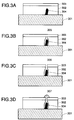
- Figs. 3A, 3B, 3C and 3D are schematic views showing each process of defect sealing according to the present invention.
- Figs. 4A, 4B, 4C and 4D are schematic views showing each process of defect sealing according to the present invention.
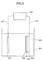
- Fig. 5 is a schematic constitution of an electrodeposition apparatus.
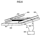
- Fig. 6 is a schematic view showing an apparatus for forming treatment.
- Fig. 7 is a schematic view showing an apparatus for passivation treatment.
- Fig. 8 is a schematic constitutional view of an apparatus suitable for the electrodeposition by a roll-to-toll method.
- FIG. 1A is a cross-sectional view of an amorphous silicon type solar cell in which light is incident from the semiconductor region side on the substrate
- Fig. 1B is a plan view of the solar cell of Fig. 1A, as viewed from the light incident side.
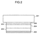
- Fig. 2 is a thin film solar cell made of amorphous silicon deposited on a translucent substrate such as glass, wherein light penetrates through an insulating substrate such as glass.
- 101, 201 are substrates, 102, 202 are lower electrodes (a conductive layer), 103, 203 are n-type semiconductor regions, 104, 204 are i-type semiconductor regions, 105, 205 are p-type semiconductor regions, 106, 206 are upper electrodes (transparent conductive layers), 107 is a grid electrode, and 108 is a bus bar.
- the substrates 101, 201 are members for mechanically supporting the semiconductors 103, 104, 105, 203, 204, 205 in the thin film solar cell made of amorphous silicon.
- the substrate When the substrate is electrically conductive, it can be also used as the electrode.
- the substrates 101, 201 are required to have a heat resistance to withstand the heating temperature when forming the semiconductor film, but may be electrically conductive or insulating.
- Specific examples of electrically conductive materials include metals such as Fe, Ni, Cr, Al, Mo, Au, Nb, Ta, V, Ti, Pt, Pb, Ti, or their alloy, for example, a thin plate made of brass or stainless steel, and its complex, carbon sheet, and galvanized sheet iron.
- electrically insulating materials include films or sheets made of a heat resisting synthetic resin such as polyester, polyethylene, polycarbonate, cellulose acetate, polypropylene, polyvinylchloride, polyvinylidene chloride, polystyrene, polyamide, polyimide, or epoxy, or their complex with glass fiber, carbon fiber, boron fiber, or metallic fiber, a thin plate of such a metal or a resin sheet with the surface coated with a metallic thin film of a dissimilar material and/or an insulating thin film of SiO 2 , Si 3 N 4 , Al 2 O 3 , AlN by sputtering, vapor deposition or galvanizing, glass, and ceramics.
- a heat resisting synthetic resin such as polyester, polyethylene, polycarbonate, cellulose acetate, polypropylene, polyvinylchloride, polyvinylidene chloride, polystyrene, polyamide, polyimide, or epoxy, or their complex with glass fiber, carbon fiber, boron fiber
- the lower electrodes (conductive layers) 102, 202 are provided on the opposite side of the light incident side to the semiconductors 103, 104, 105, 203, 204, 205 to take out the generated electric power, and are required to have a work function of making ohmic contact with the semiconductors 103, 203.
- the materials may include so-called metallic simple substances such as Al, Ag, Pt, Au, Ni, Ti, Mo, W, Fe, V, Cr, Cu, stainless, brass, nichrome, SnO 2 , In 2 O 3 , ZnO, ITO, or their alloy, and transparent conductive oxides (TCO).
- the surface of lower electrode is preferably smooth but may be irregular if irregular reflection of light is desired to occur. In the constitution of Figs. 1A and 1B, when the substrate 101 is electrically conductive, it is unnecessary to provide the lower electrode 102 specifically.
- the semiconductor for photovoltaic element for use with the present invention may be a compound semiconductor such as pin junction non-single crystal silicon, pn junction polysilicon and CuInSe 4 /CdS.
- examples of the semiconductor material constituting i-type semiconductor regions 104, 204 may include a-Si:H, a-Si:F, a-Si:H:F, a-SiGe:H, a-SiGe:F, a-SiGe:H:F, a-SiC:H, a-SiC:F, or a-SiC:H:F for so-called IV-group or IV-group alloy amorphous semiconductors.
- the photovoltaic element which is obtained according to the present invention is applicable to a so-called tandem cell or triple cell wherein two or more layers of semiconductor junction are laminated for the purpose of improving the spectral sensitivity or voltage.
- Under electrodes (transparent conductive layers) 106, 206 are electrodes for taking out the electromotive force generated by the semiconductor, and are paired with respective lower electrodes.
- Such an upper electrode is required for the semiconductor having a high sheet resistance, such as amorphous silicon type semiconductor, but is not specifically required for the crystal-type solar cell because of its low sheet resistance.
- the upper electrode must be transparent because it is located on the light incident side, and thus is referred to as a transparent electrode.
- the upper electrode desirably has a light transmittance of 85 % or greater to allow sun light or the light from a white fluorescent lamp to be absorbed efficiently into the semiconductor, and further desirably has an electrical sheet resistance of 100 ⁇ / ⁇ or less to allow the current generated by light to flow across the semiconductor transversely.
- the materials having such characteristics may include metallic oxides such as SnO 2 , In 2 O 3 , ZnO, CdO, CdSnO 4 , and ITO (In 2 O 3 +SnO 2 ).
- Electrodeposition resin is used to insulate the short or shunt portion generated by various defects such as a pinhole, grain boundary, and a spike-like defect in the substrate 101 and the lower electrode 102 (or an upper electrode 206), and further has an additional feature of improving the moisture resistance.
- the shunt resistance of solar cell is ideally infinite, but the conversion efficiency of solar cell is not affected by a shunt resistance of about 10 3 to 10 6 ⁇ cm 2 . However, if a shunt or short is present due to defect, with a shunt resistance of 1K ⁇ cm 2 or less, the conversion efficiency will remarkably decrease.
- Electrodeposition resin must be deposited directly on the defective portion.
- the electrodeposition process may be made immediately after the formation of semiconductor 105, 203 to prevent adequately the occurrence of defects in the semiconductor, or after the formation of an upper electrode 106 (or a lower electrode 202).
- the skeletal resin for electrodeposition resin having insulating and moisture proof properties is appropriately selected as desired from acrylic resin, polyester resin, epoxy resin, urethane resin, fluororesin, melamine resin, and butadien resin. Also, to effect electrophoresis for such resin in an aqueous solution, it is necessary to introduce a functional group for ionizing the resin to produce ions in the aqueous solution. Examples of the functional group may include a carboxyl group and an amino group. Electrodeposition paints with the above-cited resin dispersed can be classified into a cation type and an anion type in accordance with the polarity of a functional group. Based on a different polarity, they are appropriately selected in accordance with the desired characteristic.
- a functional group of causing a crosslinking reaction such as melamine crosslinking, carbon-carbon double bond or urethane bond, should be appropriately introduced into the skeletal resin or side chain.
- the film of electrodeposition resin is preferably not formed on other than the defective portion of solar cell, for which it is required that unnecessary paint is easily washed off after electrodeposition. Accordingly, the minimum film forming temperature (MFT) as desired is 50°C or greater.
- the resin is stably suspended in the solution without precipitation.
- the resin is desirably in the form of micell of an appropriate size.
- the grain diameter of the micell is desirably from about 10 to 100nm, desirably in the monodispersed system.
- the molecular weight of skeletal resin constituting the micell is preferably about 1000 to 20000 in the number average molecular weight.
- a filler such as an inorganic pigment, ceramics, glass frit, and particulate polymer is dispersed in the electrodeposition resin, and it is preferred that such filler is appropriately selected as desired.
- a greater electrodeposition film weight per unit quantity of electricity is preferable, for which Coulomb efficiency of electrodeposition paint is preferably 10mg/C or greater.
- the solvent of electrodeposition paint used may be a solution containing an acid or alkali having a concentration at which solar cell components such as a transparent electrical conductor, a semiconductor region and a conductor are not readily dissolved, or a solution containing metallic salt thereof.
- metallic salt may be composed of a metal having a negative normal electrode potential, wherein the hydrogen overvoltage is smaller than the absolute value of normal electrode potential.
- Electrodeposition paint is used by diluting it with deionized water, the preferable range for film formation containing a solid component of 1% to 25%.
- the electrical conductivity of liquid is desirably in a range of about 100 ⁇ S/cm to 2000 ⁇ S/cm, so that the resin can be stably suspended, easily bringing about electrophoresist, and readily allowing deposition on the desired defective portion.
- the solvent is used or the thermal process is performed, after electrodeposition, in which it is preferred that the deposited electrodeposition film is not affected by such treatment.
- the defective portion of solar cell itself does not contribute to the power generation, but even when the electrodeposition film is selectively deposited, there is a possible instance where the film may be deposited in a wider area than the substantial area of a defective portion, for which it is preferable-that the electrodeposition paint is of a light transmissive material so as not to prevent light from entering the normal portion. Further, considering various environments where the solar cell is used outdoors, excellent weather resistance, and the stability against heat, humidity and light are required.
- the solar cell since the solar cell may be flexed or impacted during use in some cases, it is preferred that the solar cell has a mechanical strength and a peel strength.
- the thickness of electrodeposition film can be appropriately selected depending on the kind of resin, considering that the electrical insulating property and the moisture resistance should be retained and the light transmissivity with the photovoltaic element must not be impaired, but typically it is preferable to have a thickness from approximately 500nm to 50 ⁇ m.
- Grid electrode 107 is an electrode for taking out the electromotive force generated in the semiconductor regions 103, 104, 105, and referred to as a collector electrode.
- the grid electrode 107 has a suitable arrangement determined from the sheet resistance of semiconductor 105 or upper electrode 106, but is formed in substantial comb-type, wherein it is preferable that the grid electrode is narrow with respect to the light incident plane and high in the light incident direction not to prevent light incidence.
- the grid electrode has preferably a specific resistance of 10 -2 ⁇ cm to 10 -5 ⁇ cm, which is not a series resistance with the solar cell.
- Examples of the material of the grid electrode include metallic materials such as Ti, Cr, Mo, W, Al, Ag, Ni, Cu, Sn, and conductive pastes composed of a power of metal such as Ag, Pt, Cu, C and an alloy thereof with polymer binder or binder solvent blended therein at an appropriate ratio to form a paste.
- Bus bar 108 for use in the present invention is an electrode for further collecting the current flowing through the grid electrode 107 to one end.
- electrode material may include metals such as Ag, Pt and Cu, or C, and their alloy, in which a wire- or foil-like electrode is pasted, or the same conductive paste as the grid electrode 107 may be used.
- Such foil may be, for example, a copper foil, a tin-plated copper foil, or a foil with adhesive in some cases.
- the solar cell as fabricated above is formed as a module by encapsulation with any of well-known methods in order to retain an excellent weather resistance and a mechanical strength in outdoor uses.
- a specific example of encapsulation material for use is preferably EVA (ethylene-vinyl-acetate) from the respects of adhesiveness, weather resistance, and cushioning property with the solar cell for the adhesive layer.
- EVA ethylene-vinyl-acetate
- a surface protective layer made of fluorine-type resin is laminated.
- fluorine-type resin may include, for example, a polymer TFE of tetrafluoroethylene (Teflon, manufactured by Du Pont), a copolymer ETFE of tetrafluoroethylene and ethylene (Tefzel, manufactured by Du Pont), polyvinyl fluoride (Tedler, manufactured by Du Pont), and polychlorofluoroethylene CTFE (Neofron, manufactured by Daikin Kogyo).
- the weather resistance can be improved by adding an ultraviolet absorbent to such resin.
- the method of laminating such resin on the solar cell substrate may include laminating it by heat in vacuum, using an apparatus available in the market such as a vacuum laminator.
- the fabrication method of a photovoltaic element according to the present invention relies on any one of well-known methods as far as the fabrication of a semiconductor (an n-type semiconductor region, an i-type semiconductor region, a p-type semiconductor region), a lower electrode, an upper electrode, a grid electrode, and a bus bar is concerned.
- the film formation method for semiconductor may be selected as desired from the methods such as vapor deposition, sputtering, RF plasma CVD, mic-rowave plasma CVD, ECR, heat CVD, and LPCVD.
- the semiconductor is formed, for example, by plasma CVD with a silane gas for non-single crystal silicon, by sheet formation of molten silicon for polycrystalline silicon, or by deposition such as electron beam deposition, sputtering or electrolysis of electrolyte for CuInSe 4 /CdS.
- a plasma CVD method is preferably adopted in which a source gas is decomposed by plasma and deposited on the substrate.
- chemical reactor, a batch system or a continuous film forming system can be used as desired.
- the fabrication of valence controlled semiconductors can be achieved by introducing and decomposing a PH 3 or B 2 H 6 gas containing constituent atom such as phosphorus or boron, together with silane gas.
- the semiconductor material constituting the p-type semiconductor region or n-type semiconductor region suitably used with the photovoltaic element of the invention can be obtained by doping-a valence control agent into a semiconductor material constituting the i-type semiconductor region.
- the valence control agent used for the p-type semiconductor may be a compound containing an element of III-group in the periodic table.
- III-group element may include B, Al, Ga, and In.
- the valence control agent for the n-type semiconductor may be a compound containing an element of V-group in the periodic table.
- V-group element may include P, N, As, and Sb.
- Lower electrode is fabricated by plating, vapor deposition or sputtering.
- the fabrication method of the upper electrode is appropriately selected as desired from the methods such as resistance heating vapor deposition, electron beam heating vapor deposition, sputtering, and spraying.
- the forming treatment is a process of decreasing greatly the electrical resistance at the defective portion by applying a voltage between the conductive layer and the semiconductor region (or a transparent conductive layer) of a photoelectric conversion element having the conductive layer and the semiconductor region (or further transparent conductor) formed on the substrate to subject the defective portion (having a lower electrical resistance than its surroundings) to dielectric breakdown selectively and compulsorily.
- the applied voltage is in a range of approximately 2 to 10V which is substantially applied between the conductive layer and the semiconductor layer (or a transparent conductive layer), wherein it is necessary to select a voltage at which the normal portion of the photoelectric conversion element does not undergo dielectric breakdown.
- the applied current used is reverse-bias direct current or current alternating between forward-bias and reverse-bias at a predetermined period with respect to the photoelectric conversion element.
- 601 is a photoelectric conversion element to which forming treatment is applied, and is placed on an electrically conductive carrier board 602 with a substrate down for the electrical connection between the conductive layer and the carrier board.
- 603 is a power source
- 604 is a conductive lead
- 605 is a driver portion for a voltage applier
- 606 is the voltage applier.
- the voltage applier serves to apply a voltage to the surface of semiconductor (or a transparent conductive layer) left in slight contact state, as well as applying a uniform voltage to the entire surface of the photoelectric converter 601 while moving in parallel to the photoelectric converter 601.
- the voltage applier is preferably fabricated by using an electrically conductive soft brush or rubber roller which imposes no damage on the surface of the photoelectric converter 601.
- the relative movement rate (forming treatment rate) between the voltage applier and the photoelectric converter should be as fast as possible from the viewpoint of productivity, and is preferably in a range from about 20cm/min to 300cm/min to assure the reliable treatment.
- the photoelectric conversion element 601 can be moved, with the voltage applier 606 fixed, to the same forming effect. This latter is effective, particularly when the photovoltaic element by roll to roll method is moved.
- the short passivation treatment is to electrochemically reduce selectively the defective portion of a photoelectric converter having a conductive layer, semiconductor regions, and a transparent conductive layer formed in sequence on the substrate, thereby dissolving and removing partially or entirely the material at the defective portion.
- An example of electrolytic apparatus to be used is illustrated in a schematic view of Fig. 7.
- An electrolytic bath 701 is filled with an electrolyte 702.
- An anode 703 electrically connected to a conductive member 707 and a cathode as a photoelectric converter are immersed in the bath.
- the conductive member 707 is connected to a DC power source 706.
- the conductive member on the cathode side is electrically connected to the conductive layer of photovoltaic element.
- the electrolyte may be an acid solution such as hydrochloric acid, nitric acid or sulfuric acid, an alkaline solution such as sodium hydroxide or potassium hydroxide, or a metallic salt solution, having a concentration at which the transparent conductive layer is not easily dissolved.
- Such metallic salt may be a salt composed of a metal having a negative normal electrode potential, in which the hydrogen overvoltage is smaller than the absolute value of normal electrode potential.
- examples thereof include aluminum chloride, magnesium sulfate and sodium chloride.
- the electrical resistance of electrolyte needs to be sufficiently low, and is preferably set in a range from about 0.05 to 1.0S/cm.
- the materials for the anode 703, which is a counter electrode, may include platinum, titanium and graphite.
- the voltage to be applied to the cathode needs to be 2V or greater, considering the hydrogen overvoltage.
- the electrolytic current density is preferably from 0.1 to 50mA/cm 2 to prevent the side reaction.
- anode 703 which is an anode electrode and the cathode which is a photoelectric converter are immersed in the electrolyte
- the anode and the cathode are only necessary to be placed via the interposition of the electrolyte, and specifically it will be appreciated that an anode vessel may be provided which is electrically connected to the power source 706 and contains an electrolyte therein, and the photoelectric converter is moved in contact with the surface of the electrolyte to dissolve the defective portion to be removed.
- the process of selectively depositing the electrodeposition resin on the defective portion is performed by immersing a photovoltaic element having the defective portion and a counter electrode in the electrodeposition paint, and applying a voltage between the photovoltaic element and the counter electrode to deposit an electrodeposition film on the defective portion.
- a schematic electrodeposition vessel is illustrated in Fig. 5.
- Fig. 5 shows an example of conducting electrodeposition treatment for the photoelectric covnerter having an upper electrode formed thereon.
- 501 is an electrolyte bath
- 502 is an electrodeposition paint liquid
- 503 is a counter electrode
- 504 is an electrically conductive substrate (substrate provided with a low electrode thereon)
- 505 is a semiconductor region
- 506 is a power source
- 507 is an electrically conductive member connecting respective electrodes to the power source 506, and 508 is a transparent conductive layer which is an upper electrode.
- the terminal from the photovoltaic element may be drawn out of the conductive substrate or the lower electrode, as shown in Fig. 5.
- the material of the counter electrode 503 is required not to be corroded in the electrodeposition paint, wherein preferable examples thereof include platinum, nickel, and stainless which are corrosion resistant. Also, it is necessary for even electrodeposition that the area of the counter electrode 503 is at a fixed ratio relative to the area of solar cell, and it is preferable that the ratio of the photovoltaic element area to the counter electrode area, or a so-called electrode ratio, is in a range from 1/2 to 2/1.
- the anode-cathode distance between the photovoltaic element and the counter electrode 503 is an important factor for retaining the evenness of electrodeposition, the preferable range in view of various conditions such as the electric conductivity of electrodeposition paint 502 or the applied voltage being typically from 10mm to 100mm.
- the substrate and other conductive portions to the electrodeposition paint 502, when the substrate 504 is electrically conductive. Therefore, it is desirable that the surface of a conductive substrate 504 which is a back face of the photovoltaic element opposite the light incident side is covered with an insulating material such as a plastic film or a rubber magnet, or the electrodeposition paint and the photoelectric converter are only brought into contact. Also, if the photovoltaic element is illuminated by light, the normal portion other than the defective portion has its resistance reduced by photoelectromotive force, resulting in a lower ratio of the resistance of the defective portion to that of the normal portion, and thus a lower selectivity. Accordingly, it is possible to provide a desired selectivity by conducting the electrodeposition in the darkness if necessary.
- the electrodeposition can be made either through a constant voltage or constant current anodizing process, but in the constant voltage anodizing process, for example, the votlage to be applied to the photovoltaic element should be a voltage at or above a hydrogen generating voltage which is calculated from the electrode voltage defined by Nernst's equation, and more specifically, a voltage which is the sum of a theoretical decomposition voltage of water plus an overvoltage, or 2 volts or greater.
- the preferable voltage range may be different, depending on the electrical conductivity of electrodeposition paint or whether the polarity of the voltage applied to the photovoltaic element is reverse-biased or forward-biased, and thus can be determined substantially in a range from about 2V to 200V, in view of various respects such as the constitution and area of solar cell, the material property such as the electrical conductivity of electrodeposition paint, the polarity of applied voltage, and the degree of light quantity (the dielectric breakdown voltage will vary in reverse-bias).
- the voltage must be within a range in which the photovoltaic element does not undergo dielectric breakdown, when reverse-biased.
- the photovoltaic element has a forward current flowing therethrough, with the selectivity degraded, so that the electrodeposition film may be likely deposited on the portion other than the defective portion. From this respect, the voltage not impairing the selectivity must be set.
- the current density is preferably in a range from 0.1 to 10A/cm 2 , depending on the shunt degree of the photovoltaic element, to form a dense electrodeposition film.
- the way of determining the termination of electrodeposition relies on using the time or the coulomb quantity. Since the electrodeposition paint film having a high resistance will not be formed in the portion reaching a certain film thickness, it is possible that electrodeposition is automatically terminated on the defective portion, depending on the constitution of photovoltaic element, thereby allowing no current to flow. However, when a forward bias is applied to the photovoltaic element, the deposition will extend over the normal portion with the elapse of time, even though some selectivity may exist at the early time of electrodeposition, whereby it is preferable to control the termination of electrodeposition with the time or the coulomb quantity, as previously described.
- a photovoltaic element 807 is an nip-type amorphous silicon deposited on a stainless substrate, on which an upper electrode of ITO is formed.
- the photovoltaic element 807 is delivered from a delivery roll 801 consecutively and immersed in an electrodeposition vessel 803, whereby a voltage is applied with respect to a counter electrode 806. It is passed through a cleaning vessel 804 and a drying furnace and then wound around a take-up roll 802.
- a masking film for the back surface of photovoltaic element is delivered from a plastic film roll not shown and bonded with the back surface of the photovoltaic element. After completion of the electrodeposition, it is peeled off again and wound after cleaning and drying. A voltage is applied between a conductive roller 808 in contact with the substrate of photovoltaic element and the counter electrode 806 installed within the electrodeposition vessel.
- 301 is a conductive substrate
- 302 is a semiconductor region
- 303 is a transparent conductive layer
- 304 is a defective portion.
- Fig. 3B illustrates a state after the forming treatment, in which 305 is a portion with reduced electrical resistance near the defective portion by the forming treatment.
- Fig. 3C illustrates a state after the short passivation process, in which 306 is a portion with lower electrical resistance which is dissolved and removed by short passivation.
- Fig. 3D illustrates a state after the electrodeposition processing, in which 307 is a sealed cavity and defective portion formed by the short passivation, which is sealed by an electrodeposition resin.
- 401 is a conductive substrate
- 402 is a semiconductor region
- 403 is a defective portion
- Fig. 4B illustrates a state after the forming process, in which 404 is a portion with reduced electrical resistance near the defective portion by the forming.
- Fig. 4C illustrates a state after the resin electrodeposition process, in which 405 is an electrodeposition portion.
- Fig. 4D illustrates a state after ITO deposition, in which 406 is an ITO deposited on the resin with the semiconductor layer and the defective portion sealed.
- the semiconductor region and the transparent conductive layer are formed on the conductive substrate, it will be appreciated that the transparent conductive layer, the semiconductor regions and the conductive layer are formed on the transparent substrate, as previously described.
- the methods of forming the grid electrode 107 in comb-like shape include vapor deposition such as sputtering, resistance heating or CVD, patterning by etching after vapor deposition of a metallic layer over the entire face, forming directly a grid electrode pattern with photo assisted CVD, plating after forming the mask of the grid electrode pattern, and printing the conductive paste.
- Electrode of conductive paste can be fabricated with good productivity by using the screen printing method.
- the screen printing method is a method in which the electrically conductive paste is used as the print ink with a screen having a desired pattern applied on the mesh of nylon or stainless, the width of the electrode being about 50 ⁇ m at minimum.
- the printing machine is preferably a screen printing machine.
- the conductive paste subjected to screen printing is heated in a drying furnace for the crosslinking of binder and the volatilization of a solvent.
- a solar cell having a layer constitution as shown in Fig. 1A was fabricated.
- a substrate 101 (30cm x 30cm, 0.2mm thick) manufactured by SUS430BA which has been subjected to sufficient degreasing and washing, was placed within a DC sputtering apparatus (not shown) in which a lower electrode 102 was formed by depositing Cr 200nm thick.
- the substrate 101 was taken out and placed within an RF plasma CVD film forming apparatus (not shown) for the deposition of an n-type semiconductor region 103, an i-type semiconductor region 104, and a p-type semiconductor region 105 in this sequence.
- an alloy of In and Sn was vapor-deposited by resistance heating in a vapor deposition apparatus with resistance heating (not shown) to deposit a 70nm thick transparent upper electrode 106 having antireflection effect, whereby the solar cell was fabricated.
- the solar cell was formed in the forming treatment apparatus of Fig. 6.
- the applied voltage was 3V of reverse bias in direct current, with the processing rate being 180cm/min.
- the solar cell after the forming treatment was subjected to passivation treatment in a short passivation apparatus of Fig. 7.
- 10% AlCl 3 aqueous solution was filled in an electrolytic bath, and the back side of the solar cell was covered with an insulating film made of plastic, and immersed in the electrolytic bath of Fig. 7.
- a voltage of minus 4V was applied to the side of a conductive substrate for the solar cell, and held for three seconds. In this process, ITO of the shunt portion and part of the defective portion were removed. After washing, drying was conducted.
- the substrate 504 for the solar cell which had undergone various treatments as previously mentioned was covered on the back surface side thereof with an insulating film of plastic, and immersed in the electrolytic bath of Fig. 5 so that the back surface of the substrate 504 was not subjected to electrodeposition.
- the counter electrode 503 used was an SUS304 stainless plate as large as 30cm x 30cm, with the back surface of the substrate 504 sealed using an insulating film made of plastic.
- the electrodeposition paint 502 used was acrylic-type cation electrodeposition paint containing a 20% solid component. A minus 10V voltage was applied to the substrate 504, and held for ten seconds to conduct electrodeposition.
- the solar cell was pulled up from the electrolytic bath, washed fully with pure water to wash off unreacted electrodeposition paint, placed in an oven at 50°C, and left for thirteen minutes to dry out water contents. Thereafter, the temperature of the oven was elevated at a rate of 10°C/min, and held for thirty minutes after reaching 180°C, to cure the electrodeposition resin.
- the solar cell was taken out of the oven, and after cooling, a part of the solar cell was cut out.
- the observation for the surface of ITO by a scan-type electron microscope showed that semi-spherical deposits, about 5 ⁇ m to 30 ⁇ m in diameter, were spotted on the surface of the ITO508.
- the infrared absorption spectrum analysis using an FTIR with microscopic feature on that portion confirmed that there was absorption peculiar to acrylic resin, and electrodeposition paint was deposited.
- OBIC an optical excitation current microscope
- 2LM21 scan-type laser microscope manufactured by Laser Tec confirmed that only the deposited portion of electrodeposition paint generated no power so that the film was deposited only on the shunt portion.
- the solar cell after the electrodeposition process was installed on a screen printing machine (not shown) in which grid electrodes 107, 100 ⁇ m wide and 8 cm long, were printed at an interval of 1 cm.
- the conductive paste contained 70 parts of Ag filter, 30 parts of polyester binder (volume ratio), and 20 parts of ethyl acetate as the solvent. After printing, the solar cell was placed in the oven, and held at 150°C for thirty minutes to cure the conductive paste.
- bus bar 108 of copper foil with an adhesive 5 mm wide as shown in Fig. 1B was bonded to fabricate a single cell of 30 cm square. With the same method, ten samples were fabricated.
- the initial characteristics of the solar cell module obtained were measured as follows.
- the reliability test for these samples was conducted based on a temperature and humidity cycle test A-2 defined in the environmental test method and the durability test method for crystal-type solar cell modules according to Japanese Industrial Standards C8917.
- thermo-hygrostat capable of controlling the temperature and humidity
- the cycle test of changing the temperature from -40°C to +85°C (relative humidity of 85%) was repeated 10 times.
- the solar cell characteristics were measured in the same way as at the initial time, using a simulator, so that the conversion efficiency was 95% in average of the initial conversion efficiency, with no significant degradation.
- the shunt resistance was measured, so that it decreased about 10%, with no significant degradation. From these points, it could be found that a series of processings of the present invention had excellent effects.
- the sealing of defects for the solar cell was conducted in the same way and procedure as the example 1-1, except that in the electrodeposition, the electrodeposition paint used an acrylic-type anion electrodeposition paint containing 10% solid component, and a plus voltage of 10 V was applied to the substrate.
- a solar cell module was fabricated.
- the measurement for the shunt resistance for obtained solar cell module showed 500 K ⁇ cm 2 to 300 K ⁇ cm 2 , with excellent characteristic and less dispersion. Also, the conversion efficiency was 6.1% ⁇ 0.5%, with excellent characteristics and less dispersion.
- the solar cell characteristics after completion of test was 95% in average of the initial conversion efficiency, with no significant degradation. Also, the shunt resistance was measured, so that it decreased about 10%, with no significant degradation. From these points, it could be found that a series of processings of the present invention had excellent effects.
- a solar cell with the same constitution as in the example 1 was fabricated in the following way, without forming, short passivation and electrodeposition.
- the portions up to the upper electrode 106 were fabricated on a substrate 101.
- grid electrodes 107 were printed in the same way.
- a copper foil with adhesive was laminated as the bus bar 108, so that a single cell of 30 cm square was fabricated.
- the reliability test for this sample was evaluated in the same way as in the example 1. After the completion of temperature and humidity cycle test, the solar cell characteristics were measured, so that the conversion efficiency was 86% of the initial value, with significant degradation indicated. Also, the measurement of shunt resistance indicated a decrease of about 20%, it being found that the shunt occurred after the completion of reliability test.
- the shunt portion for this sample was confirmed as follows. First, a reverse bias of 1.5 V was applied to the sample. The shunt portion had a current flowing therethrough, and was heated, but the normal portion, reverse-biased, has no current flowing therethrough, and thus was not heated. In this state, the observation for the surface of the sample by an infrared detection camera showed the heat generating portion, revealing that there was a shunt under the grid electrode 107.
- a transparent upper electrode 206 of SnO 2 was deposited on a glass substrate (Corning 7059) of 30 cm square, using a vapor deposition apparatus (not shown). Thereafter, the upper electrode 206 was patterned by etching so that the sub-cells 2 cm wide were arranged with a gap 5 mm wide spaced. Next, using a metal mask, p-type semiconductor region 205, i-type semiconductor region 204, n-type semiconductor region 203 were deposited to substantially overlie over the upper electrode 206.
- the substrate 201 having deposited up to the n-type semiconductor region 203 was placed within a sputtering apparatus (not shown) using a metal mask, to fabricate a lower electrode of aluminum, so that ten series of single cell of 30 cm square were fabricated.
- the forming and short passivation treatments were conducted. Subsequently, the substrate 201 thus treated was immersed in an electrolytic bath 701 for the electrodeposition using an epoxy-type cation electrodeposition paint.
- the reliability test for this sample was evaluated in the same way as in the example 1.
- the measuremnnt for the solar cell characteristics indicated 97% of the initial value, with no degradation indicated.
- the. measurement for the shunt resistance indicated almost no change.
- a solar cell module was fabricated in the same way as in the example 2-1, except that the electrodeposition was performed using an epoxy-type anion electrodeposition paint.
- the initial characteristics for obtained solar cell module were such that the conversion efficiency was 6.0% ⁇ 1%, and the shunt resistance was from 350 to 200 K ⁇ cm 2 .
- the measurement for the solar cell characteristics indicated 97% of the initial value, with no degradation indicated. Also, the measurement for the shunt resistance indicated almost no change.
- the solar cells fabricated with the solar cell fabrication method had good yield, excellent characteristics, and high durability.
- a solar cell having a constitution as shown in Figs. 1A and 1B was fabricated substantially in the same way as in the example 1.
- a lower electrode 102 As in the example 1, on a substrate 101 (30 cm x 30 cm, 0.2 mm thick) manufactured by SUS430BA was formed a lower electrode 102.
- the substrate 101 was taken out and placed within an RF plasma CVD film forming apparatus (not shown) for the deposition of n-type semiconductor region 103, i-type semiconductor region 104, and p-type semiconductor region 105 in this sequence. Thereafter, a transparent upper electrode 106 having antireflection effect was deposited 70 nm thick.
- the back side of the substrate 101 was covered with an insulating film made of plastic in the same way as in the example 1, and immersed in an electrolytic bath of Fig. 7. Then, the insulation treatment was made using a styrene-type cation electrodeposition paint. The substrate was washed sufficiently with pure water and had electrodeposition resin cured within an oven. Thereafter, the substrate 101 was taken out of the oven, and after cooling, a bus bar 108 of copper foil with adhesive was laminated thereon to fabricate a single cell of 30 cm square. With the same method, ten sheets of sample were fabricated.
- the solar cells fabricated with the solar cell fabrication method had good yield, excellent characteristics, and high durability.
- a solar cell module was fabricated in the same way as in the example 3-1, except that the electrodeposition was performed using a styrene-type anion electrodeposition paint.
- the initial characteristics for obtained solar cell module were such that the conversion efficiency was 6.4% ⁇ 1%, and the shunt resistance was 4 ⁇ cm 2 , indicating excellent characteristics.
- the measurement for the solar cell characteristics indicated 98% of the initial value, with no degradation indicated. Also, the measurement for the shunt resistance indicated almost no change.
- the solar cells fabricated with the solar cell fabrication method had good yield, excellent characteristics, and high durability.
- a solar cell having a constitution as shown in Fig. 1 was fabricated in the process of electrodeposition after forming and short passivation treatments.
- a substrate 101 (30cm x 30cm, 0.2mm thick) manufactured by SUS430BA was formed.
- the substrate 101 was placed within an RF plasma CVD film forming apparatus (not shown) for the deposition of n-type layer 103, i-type layer 104, and p-type layer 105 in this sequence.
- a transparent upper electrode 106 having antireflection effect was deposited 70nm thick.
- the solar cells fabricated with the solar cell fabrication method had good yield, excellent characteristics, and high durability.
- a solar cell module was fabricated in the same way as in the example 4-1, except that the electrodeposition was performed using a styrene-type anion electrodeposition paint.
- the initial characteristics for obtained solar cell module were such that the conversion efficiency was 7.1% ⁇ 1%, and the shunt resistance was 4 ⁇ cm 2 , indicating excellent characteristics.
- the measurement for the solar cell characteristics indicated 98% of the initial value, with no degradation indicated. Also, the measurement for the shunt resistance indicated almost no change.
- the solar cells fabricated with the solar cell fabrication method had good yield, excellent characteristics, and high durability.
- a solar cell having a layer constitution as shown in Figs. 1A and 1B was fabricated in the following way.
- a substrate 101 (30cm x 30cm, 0.2mm thick) manufactured by SUS430BA, which has been subjected to sufficient degreasing and washing, was placed within a DC sputtering apparatus (not shown) in which a lower electrode 102 was formed by depositing Cr 200nm thick.
- the substrate 101 was taken out and placed within an RF plasma CVD film forming apparatus (not shown) for the deposition of n-type semiconductor region 103, i-type semiconductor region 104, and p-type semiconductor region 105 in this sequence.
- the solar cell was formed in the forming treatment apparatus of Fig. 6.
- the applied voltage was 2.5V of reverse bias in direct current, with the treatment rate being 200cm/min.
- the counter electrode 503 used was an SUS 304 stainless plate as large as 30cm x 30cm, with the back surface of the substrate 504 sealed using an insulating film made of plastie.
- the electrodeposition paint 502 used was an acrylic-type cation electrodeposition paint containing 20% solid component. A minus 10V voltage was applied to the substrate 504, and held for ten seconds to conduct electrodeposition.
- the solar cell was pulled up from the electrolytic bath, washed fully with pure water to wash off unreacted electrodeposition paint, placed in an oven at 50°C, and left for thirteen minutes to dry out water contents. Thereafter, the temperature of the oven was elevated at a rate of 10°C/min, and held for thirty minutes after reaching 180°C, to cure the electrodeposition resin.
- the solar cell was taken out of the oven, and after cooling, a part of the solar cell was cut out.
- the infrared absorption spectrum analysis using an FTIR with microscopic feature on that portion confirmed that there was absorption peculiar to acrylic resin, and the electrodeposition paint was deposited.
- the observation of OBIC image for this sample confirmed that only the deposited portion of the electrodeposition paint generated no power so that the film was deposited only on the shunt portion.
- the solar cell after the electrodeposition process was placed in a vapor deposition apparatus with resistance heating (not shown) in which an alloy of In and Sn was vapor deposited by resistance heating, to deposit a transparent upper electrode 107, 70nm thick having antireflection effect.
- the solar cell with ITI was installed on a screen printing machine, in which a grid electrodes 107, 100 ⁇ m wide and 8cm long, were printed at an interval of 1cm.
- the conductive paste contained 70 parts of Ag filler, 30 parts of polyester binder (volume ratio), and 20 parts of ethyl acetate as the solvent. After printing, the solar cell was placed in the oven, and held at 150°C for thirty minutes to cure the conductive paste.
- bus bar 108 of copper foil with an adhesive 5mm wide was bonded as shown in Fig. 1B to fabricate a single cell of 30cm square. With the same method, ten sheets of sample were fabricated.
- the initial characteristics of the solar cell module obtained were measured.
- the shunt resistance was 500K ⁇ cm 2 to 300K ⁇ cm 2 , indicating excellent characteristics, with less dispersion.
- the solar cell characteristic was 6.2% ⁇ 0.5%, indicating excellent characteristics and with less dispersion.
- the reliability test for the solar cell module was conducted in the same way as in the example 1. After completion of the test, the solar cell characteristic was 95% in average of the initial conversion efficiency, with no significant degradation. Also, the shunt resistance decreased about 10%, with no significant degradation. From these points, it could be found that a series of processings of the present invention had excellent effects.
- a solar cell module was fabricated in the same way as in the example 5-1, except that the electrodeposition resin used an acrylic-type anion electrodeposition resin containing 25% solid component, and a plus voltage of 10V was applied to the substrate.
- the electrodeposition resin used an acrylic-type anion electrodeposition resin containing 25% solid component, and a plus voltage of 10V was applied to the substrate.
- the initial characteristics for obtained sample were measured.
- the shunt resistance was 500K ⁇ cm 2 to 300K ⁇ cm 2 , indicating excellent characteristics, with less dispersion.
- the solar cell characteristic was 6.5% ⁇ 0.5% indicating excellent characteristics, with less dispersion.
- a solar cell with the constitution of Fig. 2 was fabricated substantially in the same way as in the example 5.
- a transparent upper electrode 206 of SnO 2 was deposited on a Corning 7059 substrate 201 of 30cm square, using a vapor deposition apparatus, not shown. Thereafter, upper electrode 206 was patterned by etching so that the subcells 2cm wide were arranged with a gap 5mm wide spaced. Next, using a metal mask, p-type semiconductor region 205, i-type semiconductor region 204, n-type semiconductor region 203 were deposited to substantially overlie over the upper electrode 206.
- the forming treatment was conducted. Subsequently, the substrate 201 thus treated was immersed in an electrolytic bath 501 for the electrodeposition using an epoxy-type cation electrodeposition paint. After washing, drying and curing, the substrate was placed in a sputtering apparatus not shown to form a lower electrode of aluminum, using a metal mask, so that ten series of single cell of 30cm square were fabricated. Further, encapsulation of this sample was conducted in the same way as in the example 1. With the above fabrication method, ten sheets of solar cell module were fabricated.
- the initial characteristics for obtained solar cell module were such that the conversion efficiency was 6.0% ⁇ 1%, and the shunt resistance was from 350 to 200K ⁇ cm 2 .
- the solar cells fabricated with the solar cell fabrication method had good yield, excellent characteristics, and high durability.
- a solar cell module was fabricated in the same way as in the example 6-1, except that the electrodeposition was performed using an epoxy-type anion electrodeposition paint.
- the initial characteristics for obtained solar cell module were such that the conversion efficiency was 6.3% ⁇ 1%, and the shunt resistance was from 350 to 200K ⁇ cm 2 .
- the measurement for the solar cell characteristics indicated 95% of the initial value, with no degradation indicated. Also, the measurement for the shunt resistance indicated almost no change.
- the solar cells fabricated with the solar cell fabrication method had good yield, excellent characteristics, and high durability.
- a solar cell having a constitution as shown in Figs. 1A and 1B was fabricated substantially in the same way as in the example 5.
- a lower electrode 102 As in the example 1, on a substrate 101 (30cm x 30cm, 0.2mm thick) manufactured by SUS430BA was formed a lower electrode 102. The substrate 101 was taken out and placed within an RF plasma CVD film forming apparatus not shown for the deposition of n-type semiconductor region 103, i-type semiconductor region 104, and p-type semiconductor region 105 in this sequence.
- the back face side of the substrate 101 was covered with an insulating film made of plastic in the same way as in the example 5, and immersed in an electrolytic bath of Fig. 5. Then, the insulation treatment was made using a styrene-type cation electrodeposition paint. The substrate was washed sufficiently with pure water and had electrodeposition resin cured within an oven. Thereafter, the substrate 101 was taken out of the oven, the after cooling, ITO as a transparent upper electrode having antireflection effect was deposited 70nm thick. Further, a bus bar 108 of copper foil with adhesive was laminated thereon to fabricate a single cell of 30cm square. With the same method, ten sheets of sample were fabricated.
- the initial characteristic of the sample obtained was 6.1% ⁇ 1%, with the series resistance being 4 ⁇ cm 2 , indicating excellent characteristics.
- the durability characteristics for this solar cell module was evaluated in the same way as in the example 1. After completion of the temperature and humidity cycle test, the measurement for the solar cell characteristic for this sample indicated 99% of the initial value, with no degradation. The measurement for the shunt resistance indicates almost no change.
- the solar cell fabricated with the solar cell fabrication method of the present invention had good yield, excellent characteristics, and high durability.
- a solar cell module was fabricated in the same way as in the example 7-1, except that the electrodeposition was performed using a styrene-type anion electrodeposition paint.
- the initial characteristic for obtained solar cell module was 6.1% ⁇ 1%, and the series resistance was 4 ⁇ cm 2 , indicating excellent characteristics.
- the durability characteristic for this sample was evaluated in the same way as in the example 1. After the temperature and humidity cycle test, the measurement for the solar cell characteristics for this sample indicated 99% of the initial value, with no degradation indicated. Also, the measurement for the shunt resistance indicated almost no change.
- a lower electrode 102 As in the example 5, on a substrate 101 (30cm x 30cm, 0.2 mm thick) manufactured by SUS430BA was formed a lower electrode 102.
- the substrate 101 was placed within an RF plasma CVD film forming apparatus not shown for the deposition of n-type semiconductor region 103, i-type semiconductor region 104, and p-type semiconductor region 105 in this sequence.
- the forming treatment was conducted in the exact same way as in the example 5. Then, the insulation treatment was made in the electrolytic bath of Fig. 5, using a fluorine-type cation electrodeposition paint.
- the substrate was washed sufficiently with pure water and cured by heating at 160°C in an oven for forty minutes. Thereafter, the substrate 101 was taken out of the oven, and after cooling, ITO as a transparent conductive layer having antireflection feature was deposited 70nm thick. Further, a bus bar 108 of copper foil with adhesive was laminated thereon to fabricate a single cell of 30cm square. In the same way, ten sheets of sample were fabricated.
- the initial characteristics of the solar cell module obtained were such that the conversion efficiency was 6.8% ⁇ 1%, with the series resistance being 4 ⁇ cm 2 , indicating excellent characteristics.
- the solar cell characteristic for the sample was 97% of the initial value, with no degradation.
- the measurement for the shunt resistance indsicates almost no change.
- the solar cell fabricated with the solar cell fabrication method of the present invention had good yield, excellent characteristics, and high durability.
- a solar cell module was fabricated in the same way as in the example 8-1, except that the electrodeposition was performed using a fluorine-type anion electrodeposition paint.
- the initial characteristics for obtained solar cell module were such that the conversion efficiency was 6.5% ⁇ 1%, and the series resistance was 4 ⁇ cm 2 , indicating excellent characteristics.
- the measurement for the solar cell characteristic for the sample indicated 96% of the initial value, with no degradation indicated. Also, the measurement for the shunt resistance indicated almost no change.
- the solar cells fabricated with the solar cell fabrication method of the present invention had good yield, excellent characteristics, and high durability.
- the defective portion is selectively insulated with an electrodeposition resin, it is possible to provide a solar cell having high shunt resistance, high photoelectric conversion efficiency, and high reliability. Also, it is possible to provide a fabrication method of solar cell with high yield, performance and reliability.
Landscapes
- Engineering & Computer Science (AREA)
- Microelectronics & Electronic Packaging (AREA)
- Electromagnetism (AREA)
- General Physics & Mathematics (AREA)
- Condensed Matter Physics & Semiconductors (AREA)
- Computer Hardware Design (AREA)
- Physics & Mathematics (AREA)
- Power Engineering (AREA)
- Manufacturing & Machinery (AREA)
- Photovoltaic Devices (AREA)
- Bipolar Transistors (AREA)
- Design And Manufacture Of Integrated Circuits (AREA)
- Semiconductor Integrated Circuits (AREA)
- Die Bonding (AREA)
Claims (10)
- Procédé de compensation de défauts dans un semiconducteur, comportant les étapes de formation d'une région de coupure diélectrique (305, 404) autour d'une partie défectueuse (304, 403) faiblement résistive d'une région semiconductrice; et
l'électrodéposition sélective de ladite région de coupure diélectrique (305, 404) avec une résine anionique ou cationique (307, 405), en vue d'une isolation, afin de former une région comprenant une région d'électrodéposition de cation ou d'anion. - Procédé selon la revendication 1, caractérisé en ce que le semiconducteur est un élément photovoltaïque.
- Procédé selon la revendication 1, caractérisé en ce que ledit élément semiconducteur est un semiconducteur non-monocristallin.
- Procédé selon la revendication 1, caractérisé en ce que la résistance en parallèle dudit élément semiconducteur est comprise entre 1 x 10³ Ωcm2 et 1 x 10⁶ Ωcm2.
- Procédé selon la revendication 1, caractérisé en ce que la dimension de ladite région comprenant une résine d'électrodéposition est dix fois ou moins celle de ladite partie défectueuse.
- Procédé selon la revendication 1, caractérisé en ce que ladite résine est transparente.
- Procédé selon la revendication 2 en combinaison avec la revendication 4 ou 5, comportant un conducteur électrique transparent (303, 406) sur ladite région semiconductrice,
ladite région comprenant une résine d'électrodéposition cationique ou anionique (307, 405) étant réduite de manière électrochimique. - Procédé selon la revendication 1, comportant les étapes suivantes:formation d'un substrat (301, 401), d'un semiconducteur (302, 402) sur ledit substrat (301, 401) et d'un conducteur électrique transparent (303, 406) sur ledit semiconducteur;comportant en outre une étape de traitement de passivation court pour dissoudre et éliminer le matériau au niveau de ladite région de coupure diélectrique, avant ladite étape d'électrodéposition sélective.
- Appareil pour la mise en oeuvre du procédé de la revendication 1, comportant un moyen de traitement de formage pour conduire à une coupure diélectrique autour d'une partie défectueuse (304, 403) faiblement résistive d'une région semiconductrice; et
un moyen d'électrodéposition pour recouvrir sélectivement, en vue de l'isolation, ladite région de coupure diélectrique (305, 404) avec une résine d'électrodéposition anionique ou cationique (307, 405). - Appareil selon la revendication 9, comportantun moyen pour la formation d'un semiconducteur (302, 402) sur un substrat (301, 401) et d'un conducteur électrique transparent (303, 406) sur ledit semiconducteur (302, 402);comportant en outre un moyen pour un traitement de passivation court en vue de dissoudre et d'éliminer le matériau au niveau de ladite région de coupure diélectrique.
Applications Claiming Priority (2)
| Application Number | Priority Date | Filing Date | Title |
|---|---|---|---|
| JP197828/92 | 1992-07-01 | ||
| JP4197828A JP2686022B2 (ja) | 1992-07-01 | 1992-07-01 | 光起電力素子の製造方法 |
Publications (2)
| Publication Number | Publication Date |
|---|---|
| EP0577108A1 EP0577108A1 (fr) | 1994-01-05 |
| EP0577108B1 true EP0577108B1 (fr) | 1997-06-04 |
Family
ID=16381021
Family Applications (1)
| Application Number | Title | Priority Date | Filing Date |
|---|---|---|---|
| EP93110466A Expired - Lifetime EP0577108B1 (fr) | 1992-07-01 | 1993-06-30 | Méthode et dispositif d'élimination de régions de court-circuit dans des éléments semiconducteurs |
Country Status (7)
| Country | Link |
|---|---|
| US (1) | US6132585A (fr) |
| EP (1) | EP0577108B1 (fr) |
| JP (1) | JP2686022B2 (fr) |
| KR (1) | KR970005153B1 (fr) |
| AT (1) | ATE154167T1 (fr) |
| AU (1) | AU667718B2 (fr) |
| DE (1) | DE69311209T2 (fr) |
Families Citing this family (54)
| Publication number | Priority date | Publication date | Assignee | Title |
|---|---|---|---|---|
| AU7083398A (en) * | 1997-05-07 | 1998-11-27 | Asahi Kasei Kogyo Kabushiki Kaisha | Solar battery and process for manufacturing the same |
| JP2001230341A (ja) * | 2000-02-18 | 2001-08-24 | Hitachi Ltd | 半導体装置 |
| WO2002095810A1 (fr) * | 2001-05-21 | 2002-11-28 | Molecular Electronics Corporation | Procede de reparation de defauts de dispositifs electroniques moleculaires |
| JP2003069055A (ja) * | 2001-06-13 | 2003-03-07 | Sharp Corp | 太陽電池セルとその製造方法 |
| US7109517B2 (en) * | 2001-11-16 | 2006-09-19 | Zaidi Saleem H | Method of making an enhanced optical absorption and radiation tolerance in thin-film solar cells and photodetectors |
| JP2004063933A (ja) | 2002-07-31 | 2004-02-26 | Canon Inc | 半導体素子及び半導体素子の製造方法 |
| WO2004050961A1 (fr) * | 2002-11-27 | 2004-06-17 | University Of Toledo, The | Cellule photoelectrochimique et systeme possedant un electrolyte liquide |
| WO2004049052A1 (fr) * | 2002-11-28 | 2004-06-10 | Konica Minolta Holdings, Inc. | Element d'ecran d'affichage, ecran affichage et procede de fabrication d'ecran affichage |
| US7667133B2 (en) * | 2003-10-29 | 2010-02-23 | The University Of Toledo | Hybrid window layer for photovoltaic cells |
| WO2005101510A2 (fr) * | 2004-04-16 | 2005-10-27 | The University Of Toledo | Passivation de shuntage electrochimique photo-assistee pour cellule photovoltaique |
| US20060089292A1 (en) * | 2004-10-22 | 2006-04-27 | Thomas Wirz | Methods for VOC reduced pretreatment of substrates and detection by luminescence |
| WO2006062510A1 (fr) * | 2004-12-07 | 2006-06-15 | Ahbee 2, Lp | Procede sans contact et appareil de mesure de resistance de feuille de jonctions p-n |
| WO2006110613A2 (fr) * | 2005-04-11 | 2006-10-19 | The University Of Toledo | Cellule d'electrolyse photovoltaique integree |
| US7772485B2 (en) * | 2005-07-14 | 2010-08-10 | Konarka Technologies, Inc. | Polymers with low band gaps and high charge mobility |
| US20080006324A1 (en) * | 2005-07-14 | 2008-01-10 | Konarka Technologies, Inc. | Tandem Photovoltaic Cells |
| US7781673B2 (en) * | 2005-07-14 | 2010-08-24 | Konarka Technologies, Inc. | Polymers with low band gaps and high charge mobility |
| US20070181179A1 (en) | 2005-12-21 | 2007-08-09 | Konarka Technologies, Inc. | Tandem photovoltaic cells |
| US8158881B2 (en) * | 2005-07-14 | 2012-04-17 | Konarka Technologies, Inc. | Tandem photovoltaic cells |
| US20070267055A1 (en) * | 2005-07-14 | 2007-11-22 | Konarka Technologies, Inc. | Tandem Photovoltaic Cells |
| US20070131270A1 (en) * | 2005-07-14 | 2007-06-14 | Russell Gaudiana | Window with photovoltaic cell |
| JP2007189199A (ja) | 2005-12-12 | 2007-07-26 | Tdk Corp | キャパシタおよびその製造方法 |
| US20080053518A1 (en) * | 2006-09-05 | 2008-03-06 | Pen-Hsiu Chang | Transparent solar cell system |
| US8008421B2 (en) | 2006-10-11 | 2011-08-30 | Konarka Technologies, Inc. | Photovoltaic cell with silole-containing polymer |
| US8008424B2 (en) | 2006-10-11 | 2011-08-30 | Konarka Technologies, Inc. | Photovoltaic cell with thiazole-containing polymer |
| KR100828254B1 (ko) * | 2006-10-27 | 2008-05-07 | 미리넷솔라 주식회사 | 태양전지용 실리콘 기판의 제조 공정 |
| JP4304638B2 (ja) | 2007-07-13 | 2009-07-29 | オムロン株式会社 | Cis系太陽電池及びその製造方法 |
| US20100304512A1 (en) * | 2007-11-30 | 2010-12-02 | University Of Toledo | System for Diagnosis and Treatment of Photovoltaic and Other Semiconductor Devices |
| JP5062684B2 (ja) * | 2008-02-13 | 2012-10-31 | シャープ株式会社 | 薄膜光電変換モジュールの製造方法および製造装置 |
| WO2009137141A2 (fr) * | 2008-02-21 | 2009-11-12 | Konarka Technologies, Inc. | Cellules photovoltaïques tandem |
| US20100043863A1 (en) | 2008-03-20 | 2010-02-25 | Miasole | Interconnect assembly |
| US8912429B2 (en) * | 2008-03-20 | 2014-12-16 | Hanergy Holding Group Ltd. | Interconnect assembly |
| US20110197947A1 (en) | 2008-03-20 | 2011-08-18 | Miasole | Wire network for interconnecting photovoltaic cells |
| WO2009120974A2 (fr) * | 2008-03-28 | 2009-10-01 | University Of Toledo | Système destiné à remplir de manière sélective des trous d'aiguille, des shunts faibles et/ou des chemins de découpe dans des dispositifs photovoltaïques et cellules photovoltaïques réalisées ainsi |
| GB2459651A (en) * | 2008-04-28 | 2009-11-04 | Quantasol Ltd | Concentrator photovoltaic cell |
| JP2010021437A (ja) * | 2008-07-11 | 2010-01-28 | Ulvac Japan Ltd | 太陽電池の製造装置およびその製造方法 |
| US8455606B2 (en) * | 2008-08-07 | 2013-06-04 | Merck Patent Gmbh | Photoactive polymers |
| US7979969B2 (en) * | 2008-11-17 | 2011-07-19 | Solopower, Inc. | Method of detecting and passivating a defect in a solar cell |
| US8318240B2 (en) * | 2008-11-17 | 2012-11-27 | Solopower, Inc. | Method and apparatus to remove a segment of a thin film solar cell structure for efficiency improvement |
| US8318239B2 (en) * | 2008-11-17 | 2012-11-27 | Solopower, Inc. | Method and apparatus for detecting and passivating defects in thin film solar cells |
| US20100264035A1 (en) * | 2009-04-15 | 2010-10-21 | Solopower, Inc. | Reel-to-reel plating of conductive grids for flexible thin film solar cells |
| JP5528929B2 (ja) * | 2009-08-31 | 2014-06-25 | 三井化学東セロ株式会社 | 測定方法、太陽電池モジュールの製造方法、太陽電池モジュールおよび太陽電池モジュールの評価方法 |
| US8356640B1 (en) | 2010-01-14 | 2013-01-22 | Mia Solé | Apparatuses and methods for fabricating wire current collectors and interconnects for solar cells |
| US9061344B1 (en) | 2010-05-26 | 2015-06-23 | Apollo Precision (Fujian) Limited | Apparatuses and methods for fabricating wire current collectors and interconnects for solar cells |
| US10026859B2 (en) | 2010-10-04 | 2018-07-17 | Beijing Apollo Ding Rong Solar Technology Co., Ltd. | Small gauge wire solar cell interconnect |
| US8951824B1 (en) | 2011-04-08 | 2015-02-10 | Apollo Precision (Fujian) Limited | Adhesives for attaching wire network to photovoltaic cells |
| US9151597B2 (en) | 2012-02-13 | 2015-10-06 | First Solar, Inc. | In situ substrate detection for a processing system using infrared detection |
| JP6049556B2 (ja) | 2013-07-01 | 2016-12-21 | 株式会社東芝 | 太陽電池、太陽電池モジュール及び太陽電池の製造方法 |
| US9564270B2 (en) * | 2013-12-27 | 2017-02-07 | Tdk Corporation | Thin film capacitor |
| JP6446877B2 (ja) | 2014-07-16 | 2019-01-09 | Tdk株式会社 | 薄膜キャパシタ |
| JP6365216B2 (ja) | 2014-10-15 | 2018-08-01 | Tdk株式会社 | 薄膜キャパシタ |
| JP6641872B2 (ja) | 2015-10-15 | 2020-02-05 | Tdk株式会社 | 電子デバイスシート |
| WO2018155938A1 (fr) | 2017-02-24 | 2018-08-30 | Lg Electronics Inc. | Cellule solaire à semi-conducteur composite et son procédé de fabrication |
| WO2019061159A1 (fr) * | 2017-09-28 | 2019-04-04 | 深圳市大疆创新科技有限公司 | Procédé et dispositif de localisation de panneau photovoltaïque défectueux et véhicule aérien sans pilote |
| US11430974B2 (en) * | 2019-05-17 | 2022-08-30 | Ppg Industries Ohio, Inc. | System for roll-to-roll electrocoating of battery electrode coatings onto a foil substrate |
Family Cites Families (7)
| Publication number | Priority date | Publication date | Assignee | Title |
|---|---|---|---|---|
| US4197141A (en) * | 1978-01-31 | 1980-04-08 | Massachusetts Institute Of Technology | Method for passivating imperfections in semiconductor materials |
| US4451970A (en) * | 1982-10-21 | 1984-06-05 | Energy Conversion Devices, Inc. | System and method for eliminating short circuit current paths in photovoltaic devices |
| US4464823A (en) * | 1982-10-21 | 1984-08-14 | Energy Conversion Devices, Inc. | Method for eliminating short and latent short circuit current paths in photovoltaic devices |
| JPS6085577A (ja) * | 1983-10-17 | 1985-05-15 | Fuji Xerox Co Ltd | 薄膜光電変換素子の製造方法 |
| US4729970A (en) * | 1986-09-15 | 1988-03-08 | Energy Conversion Devices, Inc. | Conversion process for passivating short circuit current paths in semiconductor devices |
| US4749454A (en) * | 1986-11-17 | 1988-06-07 | Solarex Corporation | Method of removing electrical shorts and shunts from a thin-film semiconductor device |
| JPH04266068A (ja) * | 1991-02-20 | 1992-09-22 | Canon Inc | 光電変換素子及びその製造方法 |
-
1992
- 1992-07-01 JP JP4197828A patent/JP2686022B2/ja not_active Expired - Fee Related
-
1993
- 1993-06-29 AU AU41610/93A patent/AU667718B2/en not_active Ceased
- 1993-06-30 EP EP93110466A patent/EP0577108B1/fr not_active Expired - Lifetime
- 1993-06-30 AT AT93110466T patent/ATE154167T1/de not_active IP Right Cessation
- 1993-06-30 DE DE69311209T patent/DE69311209T2/de not_active Expired - Fee Related
- 1993-07-01 KR KR1019930012272A patent/KR970005153B1/ko not_active IP Right Cessation
-
1996
- 1996-11-15 US US08/749,727 patent/US6132585A/en not_active Expired - Fee Related
Also Published As
| Publication number | Publication date |
|---|---|
| US6132585A (en) | 2000-10-17 |
| AU667718B2 (en) | 1996-04-04 |
| JPH0621493A (ja) | 1994-01-28 |
| ATE154167T1 (de) | 1997-06-15 |
| DE69311209D1 (de) | 1997-07-10 |
| DE69311209T2 (de) | 1998-01-15 |
| AU4161093A (en) | 1994-01-06 |
| KR940006294A (ko) | 1994-03-23 |
| KR970005153B1 (ko) | 1997-04-12 |
| JP2686022B2 (ja) | 1997-12-08 |
| EP0577108A1 (fr) | 1994-01-05 |
Similar Documents
| Publication | Publication Date | Title |
|---|---|---|
| EP0577108B1 (fr) | Méthode et dispositif d'élimination de régions de court-circuit dans des éléments semiconducteurs | |
| AU651486B2 (en) | Photoelectric conversion element and fabrication method thereof | |
| KR100325952B1 (ko) | 광기전력소자와이를제조하는방법 | |
| AU695669B2 (en) | Photovoltaic element, electrode structure thereof, and process for producing the same | |
| JP2992638B2 (ja) | 光起電力素子の電極構造及び製造方法並びに太陽電池 | |
| AU758272B2 (en) | Photovoltaic device, process for production thereof, and zinc oxide thin film | |
| KR100334595B1 (ko) | 광기전력소자의제조방법 | |
| JPH1056190A (ja) | 光起電力素子及びその製造方法 | |
| US6491808B2 (en) | Electrolytic etching method, method for producing photovoltaic element, and method for treating defect of photovoltaic element | |
| JP3078936B2 (ja) | 太陽電池 | |
| JPH06318723A (ja) | 光起電力素子およびその作製方法 | |
| JPH06151908A (ja) | 太陽電池の欠陥封止方法 | |
| JPH06140648A (ja) | 太陽電池及びその製造方法 | |
| JPH06204519A (ja) | 太陽電池 | |
| JPH06204520A (ja) | 太陽電池の欠陥部分封止法 | |
| JPH06196732A (ja) | 太陽電池 | |
| JP3078935B2 (ja) | 太陽電池の製造方法 | |
| JP3078938B2 (ja) | 太陽電池 | |
| Vijh | Triple junction amorphous silicon based flexible photovoltaic submodules on polyimide substrates | |
| AU722932B2 (en) | Photovoltaic element and method for producing the same | |
| JPH0563219A (ja) | 太陽電池及びその製造方法 | |
| JP2000188410A (ja) | 光起電力素子の製造方法 | |
| JPH06318721A (ja) | 太陽電池 | |
| JPH11145501A (ja) | 光起電力素子 | |
| JPH0846230A (ja) | 光起電力素子の電極及び光起電力素子 |
Legal Events
| Date | Code | Title | Description |
|---|---|---|---|
| PUAI | Public reference made under article 153(3) epc to a published international application that has entered the european phase |
Free format text: ORIGINAL CODE: 0009012 |
|
| AK | Designated contracting states |
Kind code of ref document: A1 Designated state(s): AT BE CH DE DK ES FR GB GR IE IT LI LU MC NL PT SE |
|
| 17P | Request for examination filed |
Effective date: 19940524 |
|
| 17Q | First examination report despatched |
Effective date: 19950509 |
|
| GRAG | Despatch of communication of intention to grant |
Free format text: ORIGINAL CODE: EPIDOS AGRA |
|
| GRAH | Despatch of communication of intention to grant a patent |
Free format text: ORIGINAL CODE: EPIDOS IGRA |
|
| GRAH | Despatch of communication of intention to grant a patent |
Free format text: ORIGINAL CODE: EPIDOS IGRA |
|
| GRAA | (expected) grant |
Free format text: ORIGINAL CODE: 0009210 |
|
| AK | Designated contracting states |
Kind code of ref document: B1 Designated state(s): AT BE CH DE DK ES FR GB GR IE IT LI LU MC NL PT SE |
|
| PG25 | Lapsed in a contracting state [announced via postgrant information from national office to epo] |
Ref country code: NL Free format text: LAPSE BECAUSE OF FAILURE TO SUBMIT A TRANSLATION OF THE DESCRIPTION OR TO PAY THE FEE WITHIN THE PRESCRIBED TIME-LIMIT Effective date: 19970604 Ref country code: LI Free format text: LAPSE BECAUSE OF FAILURE TO SUBMIT A TRANSLATION OF THE DESCRIPTION OR TO PAY THE FEE WITHIN THE PRESCRIBED TIME-LIMIT Effective date: 19970604 Ref country code: IT Free format text: LAPSE BECAUSE OF FAILURE TO SUBMIT A TRANSLATION OF THE DESCRIPTION OR TO PAY THE FEE WITHIN THE PRE;WARNING: LAPSES OF ITALIAN PATENTS WITH EFFECTIVE DATE BEFORE 2007 MAY HAVE OCCURRED AT ANY TIME BEFORE 2007. THE CORRECT EFFECTIVE DATE MAY BE DIFFERENT FROM THE ONE RECORDED.SCRIBED TIME-LIMIT Effective date: 19970604 Ref country code: GR Free format text: LAPSE BECAUSE OF FAILURE TO SUBMIT A TRANSLATION OF THE DESCRIPTION OR TO PAY THE FEE WITHIN THE PRESCRIBED TIME-LIMIT Effective date: 19970604 Ref country code: ES Free format text: THE PATENT HAS BEEN ANNULLED BY A DECISION OF A NATIONAL AUTHORITY Effective date: 19970604 Ref country code: DK Effective date: 19970604 Ref country code: CH Free format text: LAPSE BECAUSE OF FAILURE TO SUBMIT A TRANSLATION OF THE DESCRIPTION OR TO PAY THE FEE WITHIN THE PRESCRIBED TIME-LIMIT Effective date: 19970604 Ref country code: BE Effective date: 19970604 Ref country code: AT Effective date: 19970604 |
|
| REF | Corresponds to: |
Ref document number: 154167 Country of ref document: AT Date of ref document: 19970615 Kind code of ref document: T |
|
| REG | Reference to a national code |
Ref country code: CH Ref legal event code: EP |
|
| PG25 | Lapsed in a contracting state [announced via postgrant information from national office to epo] |
Ref country code: LU Free format text: LAPSE BECAUSE OF NON-PAYMENT OF DUE FEES Effective date: 19970630 |
|
| REF | Corresponds to: |
Ref document number: 69311209 Country of ref document: DE Date of ref document: 19970710 |
|
| ET | Fr: translation filed | ||
| PG25 | Lapsed in a contracting state [announced via postgrant information from national office to epo] |
Ref country code: IE Free format text: LAPSE BECAUSE OF NON-PAYMENT OF DUE FEES Effective date: 19970804 |
|
| PG25 | Lapsed in a contracting state [announced via postgrant information from national office to epo] |
Ref country code: SE Effective date: 19970904 Ref country code: PT Effective date: 19970904 |
|
| NLV1 | Nl: lapsed or annulled due to failure to fulfill the requirements of art. 29p and 29m of the patents act | ||
| REG | Reference to a national code |
Ref country code: CH Ref legal event code: PL |
|
| PG25 | Lapsed in a contracting state [announced via postgrant information from national office to epo] |
Ref country code: MC Effective date: 19971231 |
|
| PLBE | No opposition filed within time limit |
Free format text: ORIGINAL CODE: 0009261 |
|
| STAA | Information on the status of an ep patent application or granted ep patent |
Free format text: STATUS: NO OPPOSITION FILED WITHIN TIME LIMIT |
|
| 26N | No opposition filed | ||
| REG | Reference to a national code |
Ref country code: GB Ref legal event code: IF02 |
|
| PGFP | Annual fee paid to national office [announced via postgrant information from national office to epo] |
Ref country code: FR Payment date: 20050608 Year of fee payment: 13 |
|
| PGFP | Annual fee paid to national office [announced via postgrant information from national office to epo] |
Ref country code: DE Payment date: 20050623 Year of fee payment: 13 |
|
| PGFP | Annual fee paid to national office [announced via postgrant information from national office to epo] |
Ref country code: GB Payment date: 20050629 Year of fee payment: 13 |
|
| PG25 | Lapsed in a contracting state [announced via postgrant information from national office to epo] |
Ref country code: GB Free format text: LAPSE BECAUSE OF NON-PAYMENT OF DUE FEES Effective date: 20060630 |
|
| PG25 | Lapsed in a contracting state [announced via postgrant information from national office to epo] |
Ref country code: DE Free format text: LAPSE BECAUSE OF NON-PAYMENT OF DUE FEES Effective date: 20070103 |
|
| GBPC | Gb: european patent ceased through non-payment of renewal fee |
Effective date: 20060630 |
|
| REG | Reference to a national code |
Ref country code: FR Ref legal event code: ST Effective date: 20070228 |
|
| PG25 | Lapsed in a contracting state [announced via postgrant information from national office to epo] |
Ref country code: FR Free format text: LAPSE BECAUSE OF NON-PAYMENT OF DUE FEES Effective date: 20060630 |