EP0575194B1 - Method for semiconductor device having capacitor - Google Patents
Method for semiconductor device having capacitor Download PDFInfo
- Publication number
- EP0575194B1 EP0575194B1 EP93304786A EP93304786A EP0575194B1 EP 0575194 B1 EP0575194 B1 EP 0575194B1 EP 93304786 A EP93304786 A EP 93304786A EP 93304786 A EP93304786 A EP 93304786A EP 0575194 B1 EP0575194 B1 EP 0575194B1
- Authority
- EP
- European Patent Office
- Prior art keywords
- film
- dielectric film
- dielectric
- substrate
- diffusion layer
- Prior art date
- Legal status (The legal status is an assumption and is not a legal conclusion. Google has not performed a legal analysis and makes no representation as to the accuracy of the status listed.)
- Expired - Lifetime
Links
- 239000004065 semiconductor Substances 0.000 title claims description 30
- 239000003990 capacitor Substances 0.000 title claims description 28
- 238000000034 method Methods 0.000 title claims description 14
- 238000009792 diffusion process Methods 0.000 claims description 33
- 239000000758 substrate Substances 0.000 claims description 23
- 239000010936 titanium Substances 0.000 claims description 17
- RTAQQCXQSZGOHL-UHFFFAOYSA-N Titanium Chemical compound [Ti] RTAQQCXQSZGOHL-UHFFFAOYSA-N 0.000 claims description 16
- 229910052719 titanium Inorganic materials 0.000 claims description 16
- 229910052710 silicon Inorganic materials 0.000 claims description 10
- 239000010703 silicon Substances 0.000 claims description 10
- 238000004519 manufacturing process Methods 0.000 claims description 6
- 239000000203 mixture Substances 0.000 claims description 6
- 229910052751 metal Inorganic materials 0.000 claims description 4
- 239000002184 metal Substances 0.000 claims description 4
- 229910021332 silicide Inorganic materials 0.000 claims description 4
- 230000002269 spontaneous effect Effects 0.000 claims description 4
- 230000015572 biosynthetic process Effects 0.000 claims description 3
- 229910052715 tantalum Inorganic materials 0.000 claims description 3
- GUVRBAGPIYLISA-UHFFFAOYSA-N tantalum atom Chemical compound [Ta] GUVRBAGPIYLISA-UHFFFAOYSA-N 0.000 claims description 3
- WFKWXMTUELFFGS-UHFFFAOYSA-N tungsten Chemical compound [W] WFKWXMTUELFFGS-UHFFFAOYSA-N 0.000 claims description 3
- 229910052721 tungsten Inorganic materials 0.000 claims description 3
- 239000010937 tungsten Substances 0.000 claims description 3
- -1 silicide compound Chemical class 0.000 claims description 2
- 238000000151 deposition Methods 0.000 claims 2
- 239000010408 film Substances 0.000 description 145
- 239000010410 layer Substances 0.000 description 29
- BASFCYQUMIYNBI-UHFFFAOYSA-N platinum Chemical compound [Pt] BASFCYQUMIYNBI-UHFFFAOYSA-N 0.000 description 26
- VYPSYNLAJGMNEJ-UHFFFAOYSA-N Silicium dioxide Chemical compound O=[Si]=O VYPSYNLAJGMNEJ-UHFFFAOYSA-N 0.000 description 19
- NRTOMJZYCJJWKI-UHFFFAOYSA-N Titanium nitride Chemical compound [Ti]#N NRTOMJZYCJJWKI-UHFFFAOYSA-N 0.000 description 14
- 239000011229 interlayer Substances 0.000 description 13
- 229910052697 platinum Inorganic materials 0.000 description 13
- 235000012239 silicon dioxide Nutrition 0.000 description 10
- XUIMIQQOPSSXEZ-UHFFFAOYSA-N Silicon Chemical compound [Si] XUIMIQQOPSSXEZ-UHFFFAOYSA-N 0.000 description 9
- 238000010438 heat treatment Methods 0.000 description 9
- 239000000377 silicon dioxide Substances 0.000 description 9
- 230000008569 process Effects 0.000 description 8
- 229910010252 TiO3 Inorganic materials 0.000 description 7
- 229910021421 monocrystalline silicon Inorganic materials 0.000 description 7
- 229910021420 polycrystalline silicon Inorganic materials 0.000 description 7
- 230000004888 barrier function Effects 0.000 description 6
- 239000005001 laminate film Substances 0.000 description 5
- 239000000463 material Substances 0.000 description 5
- 230000001012 protector Effects 0.000 description 5
- 230000003247 decreasing effect Effects 0.000 description 4
- BPUBBGLMJRNUCC-UHFFFAOYSA-N oxygen(2-);tantalum(5+) Chemical compound [O-2].[O-2].[O-2].[O-2].[O-2].[Ta+5].[Ta+5] BPUBBGLMJRNUCC-UHFFFAOYSA-N 0.000 description 4
- 229910052581 Si3N4 Inorganic materials 0.000 description 3
- 238000010030 laminating Methods 0.000 description 3
- QGLKJKCYBOYXKC-UHFFFAOYSA-N nonaoxidotritungsten Chemical compound O=[W]1(=O)O[W](=O)(=O)O[W](=O)(=O)O1 QGLKJKCYBOYXKC-UHFFFAOYSA-N 0.000 description 3
- HQVNEWCFYHHQES-UHFFFAOYSA-N silicon nitride Chemical compound N12[Si]34N5[Si]62N3[Si]51N64 HQVNEWCFYHHQES-UHFFFAOYSA-N 0.000 description 3
- 229910001936 tantalum oxide Inorganic materials 0.000 description 3
- 239000010409 thin film Substances 0.000 description 3
- 229910001930 tungsten oxide Inorganic materials 0.000 description 3
- 229910000838 Al alloy Inorganic materials 0.000 description 2
- PXHVJJICTQNCMI-UHFFFAOYSA-N Nickel Chemical compound [Ni] PXHVJJICTQNCMI-UHFFFAOYSA-N 0.000 description 2
- KDLHZDBZIXYQEI-UHFFFAOYSA-N Palladium Chemical compound [Pd] KDLHZDBZIXYQEI-UHFFFAOYSA-N 0.000 description 2
- 230000009471 action Effects 0.000 description 2
- QVGXLLKOCUKJST-UHFFFAOYSA-N atomic oxygen Chemical compound [O] QVGXLLKOCUKJST-UHFFFAOYSA-N 0.000 description 2
- NKZSPGSOXYXWQA-UHFFFAOYSA-N dioxido(oxo)titanium;lead(2+) Chemical compound [Pb+2].[O-][Ti]([O-])=O NKZSPGSOXYXWQA-UHFFFAOYSA-N 0.000 description 2
- 238000005468 ion implantation Methods 0.000 description 2
- 238000012986 modification Methods 0.000 description 2
- 230000004048 modification Effects 0.000 description 2
- 229910052760 oxygen Inorganic materials 0.000 description 2
- 239000001301 oxygen Substances 0.000 description 2
- 230000010287 polarization Effects 0.000 description 2
- FVBUAEGBCNSCDD-UHFFFAOYSA-N silicide(4-) Chemical compound [Si-4] FVBUAEGBCNSCDD-UHFFFAOYSA-N 0.000 description 2
- 229910021341 titanium silicide Inorganic materials 0.000 description 2
- WSMQKESQZFQMFW-UHFFFAOYSA-N 5-methyl-pyrazole-3-carboxylic acid Chemical compound CC1=CC(C(O)=O)=NN1 WSMQKESQZFQMFW-UHFFFAOYSA-N 0.000 description 1
- 229910000906 Bronze Inorganic materials 0.000 description 1
- VYZAMTAEIAYCRO-UHFFFAOYSA-N Chromium Chemical compound [Cr] VYZAMTAEIAYCRO-UHFFFAOYSA-N 0.000 description 1
- 229910012463 LiTaO3 Inorganic materials 0.000 description 1
- 229910008593 TiyO3 Inorganic materials 0.000 description 1
- 229910045601 alloy Inorganic materials 0.000 description 1
- 239000000956 alloy Substances 0.000 description 1
- 229910052454 barium strontium titanate Inorganic materials 0.000 description 1
- 229910002115 bismuth titanate Inorganic materials 0.000 description 1
- 239000010974 bronze Substances 0.000 description 1
- 238000005229 chemical vapour deposition Methods 0.000 description 1
- 229910052804 chromium Inorganic materials 0.000 description 1
- 239000011651 chromium Substances 0.000 description 1
- 239000013078 crystal Substances 0.000 description 1
- 239000003989 dielectric material Substances 0.000 description 1
- 230000000694 effects Effects 0.000 description 1
- 230000006872 improvement Effects 0.000 description 1
- AMGQUBHHOARCQH-UHFFFAOYSA-N indium;oxotin Chemical compound [In].[Sn]=O AMGQUBHHOARCQH-UHFFFAOYSA-N 0.000 description 1
- 230000010354 integration Effects 0.000 description 1
- 238000002844 melting Methods 0.000 description 1
- 230000008018 melting Effects 0.000 description 1
- 230000003446 memory effect Effects 0.000 description 1
- 229910052759 nickel Inorganic materials 0.000 description 1
- 150000004767 nitrides Chemical class 0.000 description 1
- 230000001590 oxidative effect Effects 0.000 description 1
- DYIZHKNUQPHNJY-UHFFFAOYSA-N oxorhenium Chemical compound [Re]=O DYIZHKNUQPHNJY-UHFFFAOYSA-N 0.000 description 1
- 229910052763 palladium Inorganic materials 0.000 description 1
- 239000010453 quartz Substances 0.000 description 1
- 238000012827 research and development Methods 0.000 description 1
- 229910003449 rhenium oxide Inorganic materials 0.000 description 1
- 238000004904 shortening Methods 0.000 description 1
- 238000004544 sputter deposition Methods 0.000 description 1
Images


Classifications
-
- H—ELECTRICITY
- H10—SEMICONDUCTOR DEVICES; ELECTRIC SOLID-STATE DEVICES NOT OTHERWISE PROVIDED FOR
- H10D—INORGANIC ELECTRIC SEMICONDUCTOR DEVICES
- H10D1/00—Resistors, capacitors or inductors
- H10D1/60—Capacitors
- H10D1/62—Capacitors having potential barriers
- H10D1/66—Conductor-insulator-semiconductor capacitors, e.g. MOS capacitors
-
- H—ELECTRICITY
- H10—SEMICONDUCTOR DEVICES; ELECTRIC SOLID-STATE DEVICES NOT OTHERWISE PROVIDED FOR
- H10B—ELECTRONIC MEMORY DEVICES
- H10B12/00—Dynamic random access memory [DRAM] devices
- H10B12/01—Manufacture or treatment
- H10B12/02—Manufacture or treatment for one transistor one-capacitor [1T-1C] memory cells
- H10B12/03—Making the capacitor or connections thereto
- H10B12/033—Making the capacitor or connections thereto the capacitor extending over the transistor
-
- H—ELECTRICITY
- H10—SEMICONDUCTOR DEVICES; ELECTRIC SOLID-STATE DEVICES NOT OTHERWISE PROVIDED FOR
- H10B—ELECTRONIC MEMORY DEVICES
- H10B12/00—Dynamic random access memory [DRAM] devices
- H10B12/30—DRAM devices comprising one-transistor - one-capacitor [1T-1C] memory cells
- H10B12/31—DRAM devices comprising one-transistor - one-capacitor [1T-1C] memory cells having a storage electrode stacked over the transistor
-
- H—ELECTRICITY
- H10—SEMICONDUCTOR DEVICES; ELECTRIC SOLID-STATE DEVICES NOT OTHERWISE PROVIDED FOR
- H10D—INORGANIC ELECTRIC SEMICONDUCTOR DEVICES
- H10D1/00—Resistors, capacitors or inductors
- H10D1/60—Capacitors
- H10D1/68—Capacitors having no potential barriers
- H10D1/682—Capacitors having no potential barriers having dielectrics comprising perovskite structures
-
- H—ELECTRICITY
- H10—SEMICONDUCTOR DEVICES; ELECTRIC SOLID-STATE DEVICES NOT OTHERWISE PROVIDED FOR
- H10D—INORGANIC ELECTRIC SEMICONDUCTOR DEVICES
- H10D30/00—Field-effect transistors [FET]
- H10D30/60—Insulated-gate field-effect transistors [IGFET]
- H10D30/67—Thin-film transistors [TFT]
- H10D30/674—Thin-film transistors [TFT] characterised by the active materials
- H10D30/6741—Group IV materials, e.g. germanium or silicon carbide
- H10D30/6743—Silicon
- H10D30/6744—Monocrystalline silicon
-
- H—ELECTRICITY
- H10—SEMICONDUCTOR DEVICES; ELECTRIC SOLID-STATE DEVICES NOT OTHERWISE PROVIDED FOR
- H10D—INORGANIC ELECTRIC SEMICONDUCTOR DEVICES
- H10D86/00—Integrated devices formed in or on insulating or conducting substrates, e.g. formed in silicon-on-insulator [SOI] substrates or on stainless steel or glass substrates
- H10D86/201—Integrated devices formed in or on insulating or conducting substrates, e.g. formed in silicon-on-insulator [SOI] substrates or on stainless steel or glass substrates the substrates comprising an insulating layer on a semiconductor body, e.g. SOI
-
- H—ELECTRICITY
- H10—SEMICONDUCTOR DEVICES; ELECTRIC SOLID-STATE DEVICES NOT OTHERWISE PROVIDED FOR
- H10D—INORGANIC ELECTRIC SEMICONDUCTOR DEVICES
- H10D1/00—Resistors, capacitors or inductors
- H10D1/60—Capacitors
- H10D1/68—Capacitors having no potential barriers
- H10D1/692—Electrodes
- H10D1/696—Electrodes comprising multiple layers, e.g. comprising a barrier layer and a metal layer
Definitions
- the present invention relates to a semiconductor device having a capacitor using a dielectric film possessing a high dielectric constant such as a ferroelectric film.
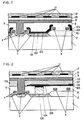
- Fig. 10 is a sectional view of this memory cell.
- numeral 1 denotes a silicon substrate
- 2 is a field oxide film (LOCOS film)
- 3 is an N + diffusion layer composing the source or the drain of transistor
- 4 is a word line composed of polycide film or polycrystalline silicon film.
- Numeral 5 is a bottom electrode made of polycrystalline silicon film connected to the diffusion layer 3
- 6 is a dielectric film laminating silicon nitride film and silicon dioxide film
- 7 is a top electrode composed of polycrystalline silicon film, and a capacitor is composed of these films.
- 5a, 6a and 7a are bumps of the bottom electrode 5, dielectric film 6, and top electrode 7, respectively.
- Numeral 8 is a first interlayer insulating film
- 9 is a first wiring for bit line made of polycide film or aluminum alloy film
- 10 is a second interlayer insulating film
- 11 is a second wiring made of aluminum alloy film
- 12 is a protector film.
- the memory cell of DRAM is usually composed of one transistor and one capacitor.
- the memory cell of a conventional DRAM is very complicated in structure because the capacitor having a necessary capacity is formed in a fine memory cell region. That is, as shown in Fig. 10, projecting portions 5a, 6a, 7a are formed in order to increase the capacity to cope with widening of the total area of the capacitor.
- Such conventional constitution involved the following problems.
- the dielectric film 6 of the capacitor in the memory cell is formed in a laminate film of silicon nitride film (relative dielectric constant about 7.5) and silicon dioxide film (relative dielectric constant about 3.9), the relative dielectric constant is small. Therefore, to form a capacitor possessing a capacity necessary for memory action, the structure and manufacturing process of the capacitor are very complicated. For example, to realize a DRAM of 64 megabits, a capacity of 30 fF is required in a memory region of about 1,5 ⁇ m 2 .
- the projecting portion 5a of the bottom electrode when the conventional laminate film of silicon nitride film and silicon dioxide film is used as dielectric film 6, if the dielectric film 6 is reduced to a thickness of 5nm as converted to silicon dioxide, the projecting portion 5a of the bottom electrode must be built up to a height of 1.5 ⁇ m. To form such high projecting portion, it requires a complicated manufacturing process comprising many process steps. Besides, leak currents are present in the junction area between P-type well and the N + diffusion layer of transistors for composing memory cell and in the dielectric film for composing the capacitor. Therefore, the refreshing cycle necessary for holding the memory data of the memory cell depend on these leak currents, it is difficult to decrease the total area of the capacitor without shortening the refresh cycle.
- EP-A-415751 shows an integrated circuit and a capacitor comprising a bottom electrode using a part of a diffusing layer, a dielectric film and a top electrode formed on a silicon substrate.
- a similar structure is shown in D.B. Slater et al. IEEE Journal of Solid-State Circuits, Vol. 24, No. 1 (1989), page 165-175 where the bottom electrode is identical with the diffusion layer (see Fig. 1c thereof).
- Fig. 1 is a partly sectional schematic view of a semiconductor device in an embodiment of the invention.
- Fig. 2 is a partly sectional schematic view of a semi-conductor device in a first example.
- Fig. 3 is a partly sectional schematic view of a semi-conductor device in a second example.
- Fig. 4 is a partly sectional schematic view of a semi-conductor device in a third example.
- Fig. 5 is a partly sectional schematic view of a semi-conductor device in a fourth example.
- Fig. 6 is a partly sectional schematic view of a semiconductor device in a fifth example.
- Fig. 7 is a partly sectional schematic view of a semi-conductor device in a sixth example.
- Fig. 8 is a partly sectional schematic view of a semi-conductor device in a seventh example.
- Fig. 9 is a partly sectional schematic view of a semi-conductor device in an eighth example.
- Fig. 10 is a partly sectional schematic view of a conventional semiconductor device.
- Fig. 1 is a sectional view showing the structure of a memory cell region of DRAM.
- numeral 101 denotes a dielectric film of Ba 1-x Sr x Ti y O 3 (0 ⁇ x ⁇ 1, y>1) containing Ti in excess of stoichiometric composition
- 102 is a dielectric film of Ba 1-x Sr x TiO 3 (0 ⁇ x ⁇ 1) in stoichiometric composition
- 103 is a top electrode composed of platinum film.
- the capacitor is formed by holding a laminate film of Ti-excess dielectric film 101 and dielectric film 102 in stoichiometric composition between the diffusion layer 3 serving also as the bottom electrode and the top electrode 103. Titanium contained in excess in the dielectric film 101 reacts, on one hand, with the spontaneous oxide film formed on the diffusion layer 3, and reacts with silicon to form a silicide compound, thereby lowering the contact resistance. On the other hand, it is also effective to improve the fitting of the dielectric film 102. Besides, by lowering the contact resistance and using the material of high dielectric constant, the total area of the capacitor may be reduced. In the capacitor, the conventional projecting portions are not needed, and the manufacturing process may be simplified.
- a dielectric film mainly composed of tantalum such as tantalum oxide (Ta 2 O 5 ) and lithium tantalate (LiTaO 3 ), or a dielectric film mainly composed of tungsten such as tungsten oxide and tungsten-bronze may be preferably used.
- tantalum oxide or tungsten oxide is relatively easy to oxidize, tantalum oxide or tungsten oxide may be easily formed on the interface with the diffusion layer 3.
- These oxides act as diffusion barrier film to prevent diffusion of silicon, the substrate material, into the dielectric film.
- the composition in the dielectric film changes continuously, so that abrupt lowering of dielectric constant may be suppressed.
- the two dielectric films 101, 102 may not be always same dielectric materials, and they may be made of different materials, such as the dielectric film 101 made of Ti-excess barium-strontium titanate and the dielectric film 102 made of lead titanate.
- the dielectric film 101 and dielectric film 102 are formed separately.
- the same object may be achieved by continuous dielectric films formed by controlling the supply titanium content and supplying the titanium excessively in the portion contacting with the diffusion layer 3 when forming the film by CVD method or sputtering method.
- the capacitor is formed on the semiconductor substrate, but the capacitor may be also formed on a semiconductor film formed on an insulating substrate or on a semiconductor thin film formed on the semiconductor substrate through an insulating layer.
- Fig. 2 is a sectional view showing the constitution of a memory cell region of other DRAM.
- numeral 104 denotes a barrier layer composed of titanium nitride (TiN)
- 105 is a bottom electrode made of platinum film
- 106 is a dielectric film of Ba 1-x Sr x TiO 3
- 107 is a top electrode made of platinum film
- 108 is a polycrystalline silicon buried in the contact hole of a first interlayer insulating film 8 made of silicon dioxide film
- 109 is a third interlayer insulating film.
- the polycrystalline silicon 108 is buried in the contact hole of the first interlayer insulating film 8 formed on the semiconductor substrate, and therefore the dielectric film 106 may be formed on the relatively flat bottom electrode 105.
- the dielectric film 106 possesses an excellent film thickness uniformity, and it is possible to reduce the film thickness furthermore in order to raise the capacity per unit area.
- the barrier layer 104 is formed between the bottom electrode 105 and polycrystalline silicon 108, it is possible to suppress the reaction between the polycrystalline silicon 108 and bottom electrode 105 in high temperature process such as heat treatment during formation of the dielectric film 106.
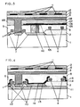
- Fig. 3 is a sectional view showing the constitution of a memory cell region of a DRAM modified from Example 1.
- Example 2 The difference of Example 2 from Example 1 shown in Fig. 2 is that a titanium nitride film 110 buried in the contact hole is directly connected to the diffusion layer 3.
- the dielectric film 106 can be formed on a relatively flat bottom electrode 105, and the dielectric film 106 possesses an excellent film thickness uniformity.
- the bottom electrode 105 and diffusion layer 3 are connected with the titanium nitride film 110, it is possible to suppress the reaction between the bottom electrode 105 and diffusion layer 3 in high temperature process such as heat treatment during formation of the dielectric film 106.
- Fig. 4 is a sectional view showing the constitution of a memory cell region in a different DRAM.
- numeral 111 is a buried silicon dioxide film formed by ion implantation of oxygen at high energy and high dose rate
- 112 is a single crystal silicon thin film formed on the buried silicon dioxide film 111
- 113 is a diffusion layer formed in the single crystal silicon film 112
- 114 is a dielectric film composed of Ba 1-x Sr x TiO 3
- 115 is a top electrode made of platinum film.
- transistors are formed in the single crystal silicon film 112 insulated and separated from the silicon substrate 1 by the buried silicon dioxide film 111, and the well forming process required in the conventional CMOS type semiconductor device is not necessary.
- the dielectric film 114 possessing a high dielectric constant the structure of the capacitor can be formed extremely simply and flatly, and the manufacturing process is notably curtailed, and improvement of yield is expected.
- the junction area of the N + type diffusion layer and P-type well is decreased in the transistor to which the capacitor is connected, and the junction leak current is significantly decreased, and the leak current in the memory cell can be decreased only to the leak current of the dielectric film 114 of the capacitor. Therefore, the cycle of the refreshing action necessary for holding the memory data of the memory cell can be extended, and the refreshing current may be decreased.
- Fig. 5 is a sectional view showing the constitution of a memory cell region of a DRAM modified from Example 3. What differs from Example 3 in Fig. 4 is that a bottom electrode 116 sequentially laminating a titanium film, titanium nitride (TiN) film and platinum film is inserted between the N + type diffusion layer 113 to be used as the source or drain of the transistor and dielectric film 114.
- the titanium film reacts with silicon by heat treatment to form silicide, and adhesion with the N + diffusion layer 113 is enhanced.
- the dielectric film 114 is an oxide
- the surface of the N + type diffusion layer 113 is oxidized by heat treatment at high temperature, but by inserting titanium film, the surface is not oxidized if heated at high temperature.
- the titanium nitride film acts as barrier film to prevent diffusion of platinum film into the diffusion layer 113.
- Example 3 same as in Example 3, it is possible to simplify the device structure, shorten the manufacturing process notably, improve the yield, extend the refreshing action cycle, and decrease the refreshing current.
- Fig. 6 is a sectional view showing the constitution of a memory cell region of a DRAM similar to the DRAM shown in Fig. 2 and Fig. 4.
- the parts same as those shown in Fig. 2 and Fig. 4 are identified with same reference numbers, and their explanations are omitted.
- numerals 117 and 118 are titanium film and titanium nitride film buried in the contact hole provided in the silicon dioxide film 8.
- the dielectric film 106 of Ba 1-x Sr x TiO 3 can be formed on the relatively flat bottom electrode 105, and the capacitor high in capacity in shape can be realized.
- the titanium film 117 reacts with the diffusion layer 113 by heat treatment to form titanium silicide, and the contact resistance is lowered.
- the titanium nitride film 118 acts as barrier film for preventing the platinum from diffusing into the diffusion layer 113 by heat treatment at high temperature in the process after forming the dielectric film 106.
- the third interlayer insulating film 109, second interlayer insulating film 10 and protector film 12 of high reliability can be formed.
- Fig. 7 is a partly sectional schematic view of a semiconductor device having a capacitor.
- numeral 121 denotes an insulating substrate made of quartz
- 122 is a single crystal silicon thin film formed on the insulating substrate 121
- 123 is a diffusion layer formed in the single crystal silicon film 122
- 124 is a dielectric film composed of Ba 1-x Sr x TiO 3
- 125 is a top electrode made of platinum.
- a selective transistor is formed on the single crystal silicon film 122 formed on the insulating substrate 121, and the well forming process required in the conventional CMOS semiconductor device is not necessary. Moreover, by using the dielectric film 124 possessing a high dielectric constant, a capacitor of a large capacity can be formed in a small area, simply and flatly.
- Fig. 8 is a partly sectional schematic view of a semiconductor device modified from Example 6. What differs from Example 6 shown in Fig. 7 is that a bottom electrode 126 sequentially laminating, from the bottom, a titanium film, titanium nitride (TiN) film, and platinum film is inserted between the N + type diffusion layer 123 as the source or drain of the transistor and the dielectric film 124. Therefore, same as in Example 4, high temperature heat treatment in the process after forming the dielectric film 124 is possible, and therefore the first interlayer insulating film 8 and protector film 12 of high reliability may be easily formed.
- TiN titanium nitride
- Fig. 9 is a partly sectional schematic view of a semi-conductor device modified from Example 7. What differs from Example 7 shown in Fig. 8 is that a bottom electrode 127 made of platinum film and diffusion layer 123 are connected through a laminated film of a titanium film 128 and titanium nitride film 129 buried in the contact hole of the second interlayer insulating film 8, and that a third interlayer insulating film 109 is formed thereon.
- the dielectric film 124 can be formed on the relatively flat bottom electrode 127, so that a highly reliable capacitor in shape can be realized.
- the titanium film 128 reacts with the diffusion layer 123 to form titanium silicide, thereby lowering the contact resistance.
- the titanium nitride film 129 acts as barrier film for preventing diffusion of platinum into the diffusion layer 123 due to heat treatment at high temperature in the process after forming the dielectric film 124.
- highly reliable third interlayer insulating film 109, second interlayer insulating film 10 and protector film 12 may be formed.
- the dielectric film possessing a high dielectric constant is a film of Ba 1-x Sr x TiO 3 , but the invention is not limited to this alone.
- Various materials such as lead titanate, PZT, PLZT, bismuth titanate, tantalum oxide, and others are also included in the invention.
- the top electrodes in Embodiment 1 and Examples 1 through 8 and the bottom electrodes in Examples 2, 5 and 8 are made of platinum film, but the invention allows to use other materials, including metal films of high melting point such as palladium, tungsten, tantalum, titanium, nickel and chromium, their alloy films, their oxide conductive films such as silicide film, indium-tin oxide (ITO), and rhenium oxide, nitride conductive films such as titanium nitride, and their laminated films.
- metal films of high melting point such as palladium, tungsten, tantalum, titanium, nickel and chromium
- their alloy films such as silicide film, indium-tin oxide (ITO), and rhenium oxide
- nitride conductive films such as titanium nitride, and their laminated films.
- Examples 3 through 5 relate to examples of a substrate having a single crystal silicon film on the oxide film formed by ion implantation of high energy and high dose rate of oxygen on the silicon substrate, and the same effects are obtained by the substrate forming a silicon single crystal film after oxidizing the silicon substrate.
- DRAM dynamic random access memory
- Examples of DRAM are shown in Embodiment 1 and Examples 2 through 5, but the invention is, needless to say, generally applicable to semiconductor devices such as a nonvolatile RAM making use of the spontaneous polarization and another semiconductor device having capacitor.
Landscapes
- Engineering & Computer Science (AREA)
- Manufacturing & Machinery (AREA)
- Semiconductor Memories (AREA)
- Semiconductor Integrated Circuits (AREA)
Priority Applications (1)
| Application Number | Priority Date | Filing Date | Title |
|---|---|---|---|
| EP97104672A EP0784347A2 (en) | 1992-06-18 | 1993-06-18 | Semiconductor device having capacitor |
Applications Claiming Priority (6)
| Application Number | Priority Date | Filing Date | Title |
|---|---|---|---|
| JP159222/92 | 1992-06-18 | ||
| JP04159222A JP3083407B2 (ja) | 1992-06-18 | 1992-06-18 | 半導体装置の製造方法 |
| JP167309/92 | 1992-06-25 | ||
| JP4167309A JPH0613573A (ja) | 1992-06-25 | 1992-06-25 | 半導体記憶装置及びその製造方法 |
| JP278380/92 | 1992-10-16 | ||
| JP4278380A JPH06132496A (ja) | 1992-10-16 | 1992-10-16 | 半導体記憶装置およびその製造方法 |
Related Child Applications (1)
| Application Number | Title | Priority Date | Filing Date |
|---|---|---|---|
| EP97104672.7 Division-Into | 1997-03-19 |
Publications (2)
| Publication Number | Publication Date |
|---|---|
| EP0575194A1 EP0575194A1 (en) | 1993-12-22 |
| EP0575194B1 true EP0575194B1 (en) | 1997-11-12 |
Family
ID=27321504
Family Applications (2)
| Application Number | Title | Priority Date | Filing Date |
|---|---|---|---|
| EP93304786A Expired - Lifetime EP0575194B1 (en) | 1992-06-18 | 1993-06-18 | Method for semiconductor device having capacitor |
| EP97104672A Withdrawn EP0784347A2 (en) | 1992-06-18 | 1993-06-18 | Semiconductor device having capacitor |
Family Applications After (1)
| Application Number | Title | Priority Date | Filing Date |
|---|---|---|---|
| EP97104672A Withdrawn EP0784347A2 (en) | 1992-06-18 | 1993-06-18 | Semiconductor device having capacitor |
Country Status (3)
| Country | Link |
|---|---|
| US (1) | US5661319A (enExample) |
| EP (2) | EP0575194B1 (enExample) |
| DE (1) | DE69315125T2 (enExample) |
Families Citing this family (23)
| Publication number | Priority date | Publication date | Assignee | Title |
|---|---|---|---|---|
| US5383088A (en) * | 1993-08-09 | 1995-01-17 | International Business Machines Corporation | Storage capacitor with a conducting oxide electrode for metal-oxide dielectrics |
| JP3683972B2 (ja) * | 1995-03-22 | 2005-08-17 | 三菱電機株式会社 | 半導体装置 |
| JP2907322B2 (ja) * | 1995-05-18 | 1999-06-21 | 日本電気株式会社 | 不揮発性半導体記憶装置 |
| JP3246274B2 (ja) * | 1995-06-22 | 2002-01-15 | 松下電器産業株式会社 | 半導体装置 |
| KR0183732B1 (ko) * | 1995-09-01 | 1999-03-20 | 김광호 | 반도체 장치의 캐패시터 제작방법 |
| KR0165484B1 (ko) | 1995-11-28 | 1999-02-01 | 김광호 | 탄탈륨산화막 증착 형성방법 및 그 장치 |
| US6555394B2 (en) | 1995-11-28 | 2003-04-29 | Samsung Electronics Co., Ltd. | Methods of fabricating capacitors including Ta2O5 layers in a chamber including changing a Ta2O5 layer to heater separation or chamber pressure |
| US5910880A (en) | 1997-08-20 | 1999-06-08 | Micron Technology, Inc. | Semiconductor circuit components and capacitors |
| US5903493A (en) * | 1997-09-17 | 1999-05-11 | Lucent Technologies Inc. | Metal to metal capacitor apparatus and method for making |
| GB2326524B (en) * | 1997-12-23 | 1999-11-17 | United Microelectronics Corp | Method of fabricating a dynamic random access memory device |
| US6191443B1 (en) | 1998-02-28 | 2001-02-20 | Micron Technology, Inc. | Capacitors, methods of forming capacitors, and DRAM memory cells |
| US6066525A (en) * | 1998-04-07 | 2000-05-23 | Lsi Logic Corporation | Method of forming DRAM capacitor by forming separate dielectric layers in a CMOS process |
| US6156638A (en) | 1998-04-10 | 2000-12-05 | Micron Technology, Inc. | Integrated circuitry and method of restricting diffusion from one material to another |
| US6730559B2 (en) * | 1998-04-10 | 2004-05-04 | Micron Technology, Inc. | Capacitors and methods of forming capacitors |
| JP2000012804A (ja) * | 1998-06-24 | 2000-01-14 | Matsushita Electron Corp | 半導体記憶装置 |
| WO2000026955A1 (en) * | 1998-10-30 | 2000-05-11 | Advanced Micro Devices, Inc. | Fabrication of a transistor having an ultra-thin gate dielectric |
| US6177305B1 (en) | 1998-12-17 | 2001-01-23 | Lsi Logic Corporation | Fabrication of metal-insulator-metal capacitive structures |
| US6391801B1 (en) | 1999-09-01 | 2002-05-21 | Micron Technology, Inc. | Method of forming a layer comprising tungsten oxide |
| US7005695B1 (en) * | 2000-02-23 | 2006-02-28 | Micron Technology, Inc. | Integrated circuitry including a capacitor with an amorphous and a crystalline high K capacitor dielectric region |
| US6303456B1 (en) | 2000-02-25 | 2001-10-16 | International Business Machines Corporation | Method for making a finger capacitor with tuneable dielectric constant |
| FR2845522A1 (fr) * | 2002-10-03 | 2004-04-09 | St Microelectronics Sa | Circuit integre a couche enterree fortement conductrice |
| JP5451011B2 (ja) * | 2008-08-29 | 2014-03-26 | ピーエスフォー ルクスコ エスエイアールエル | 半導体記憶装置及び情報処理システム |
| US10614868B2 (en) | 2018-04-16 | 2020-04-07 | Samsung Electronics Co., Ltd. | Memory device with strong polarization coupling |
Citations (2)
| Publication number | Priority date | Publication date | Assignee | Title |
|---|---|---|---|---|
| EP0380326A2 (en) * | 1989-01-26 | 1990-08-01 | Seiko Epson Corporation | Method of manufacturing a semi-conductor device |
| JPH0480959A (ja) * | 1990-07-24 | 1992-03-13 | Seiko Epson Corp | 半導体装置 |
Family Cites Families (13)
| Publication number | Priority date | Publication date | Assignee | Title |
|---|---|---|---|---|
| JPS5745968A (en) * | 1980-08-29 | 1982-03-16 | Ibm | Capacitor with double dielectric unit |
| US5519234A (en) * | 1991-02-25 | 1996-05-21 | Symetrix Corporation | Ferroelectric dielectric memory cell can switch at least giga cycles and has low fatigue - has high dielectric constant and low leakage current |
| US5053917A (en) * | 1989-08-30 | 1991-10-01 | Nec Corporation | Thin film capacitor and manufacturing method thereof |
| US5241211A (en) * | 1989-12-20 | 1993-08-31 | Nec Corporation | Semiconductor device |
| JP2898686B2 (ja) * | 1990-03-06 | 1999-06-02 | 株式会社日立製作所 | 半導体記憶装置およびその製造方法 |
| JPH0775247B2 (ja) * | 1990-05-28 | 1995-08-09 | 株式会社東芝 | 半導体記憶装置 |
| JP3092140B2 (ja) * | 1990-06-01 | 2000-09-25 | セイコーエプソン株式会社 | 半導体装置の製造方法 |
| JPH0472778A (ja) * | 1990-07-13 | 1992-03-06 | Seiko Epson Corp | 強誘電体記憶装置 |
| JP3144799B2 (ja) * | 1990-11-30 | 2001-03-12 | 松下電器産業株式会社 | 半導体装置およびその製造方法 |
| JPH0563205A (ja) * | 1991-09-03 | 1993-03-12 | Sharp Corp | 半導体装置 |
| US5206788A (en) * | 1991-12-12 | 1993-04-27 | Ramtron Corporation | Series ferroelectric capacitor structure for monolithic integrated circuits and method |
| US5313089A (en) * | 1992-05-26 | 1994-05-17 | Motorola, Inc. | Capacitor and a memory cell formed therefrom |
| US5187638A (en) * | 1992-07-27 | 1993-02-16 | Micron Technology, Inc. | Barrier layers for ferroelectric and pzt dielectric on silicon |
-
1993
- 1993-06-18 DE DE69315125T patent/DE69315125T2/de not_active Expired - Fee Related
- 1993-06-18 EP EP93304786A patent/EP0575194B1/en not_active Expired - Lifetime
- 1993-06-18 EP EP97104672A patent/EP0784347A2/en not_active Withdrawn
-
1996
- 1996-07-22 US US08/681,093 patent/US5661319A/en not_active Expired - Fee Related
Patent Citations (3)
| Publication number | Priority date | Publication date | Assignee | Title |
|---|---|---|---|---|
| EP0380326A2 (en) * | 1989-01-26 | 1990-08-01 | Seiko Epson Corporation | Method of manufacturing a semi-conductor device |
| JPH0480959A (ja) * | 1990-07-24 | 1992-03-13 | Seiko Epson Corp | 半導体装置 |
| EP0493621A1 (en) * | 1990-07-24 | 1992-07-08 | Seiko Epson Corporation | Semiconductor device |
Also Published As
| Publication number | Publication date |
|---|---|
| EP0784347A3 (enExample) | 1997-08-20 |
| DE69315125T2 (de) | 1998-06-10 |
| DE69315125D1 (de) | 1997-12-18 |
| EP0784347A2 (en) | 1997-07-16 |
| EP0575194A1 (en) | 1993-12-22 |
| US5661319A (en) | 1997-08-26 |
Similar Documents
| Publication | Publication Date | Title |
|---|---|---|
| EP0575194B1 (en) | Method for semiconductor device having capacitor | |
| US7005695B1 (en) | Integrated circuitry including a capacitor with an amorphous and a crystalline high K capacitor dielectric region | |
| US7206215B2 (en) | Antifuse having tantalum oxynitride film and method for making same | |
| US6908802B2 (en) | Ferroelectric circuit element that can be fabricated at low temperatures and method for making the same | |
| KR20000026155A (ko) | 고유전 다층막을 이용한 셀 캐패시터 및 그 제조 방법 | |
| US5506748A (en) | Capacitor for semiconductor integrated circuit | |
| JPH10275897A (ja) | 半導体装置の製造方法および半導体装置 | |
| US6740901B2 (en) | Production of semiconductor integrated circuit | |
| JP4011813B2 (ja) | 半導体装置及び半導体装置の製造方法 | |
| US6107105A (en) | Amorphous tin films for an integrated capacitor dielectric/bottom plate using high dielectric constant material | |
| KR0144921B1 (ko) | 반도체 메모리소자의 커패시터 구조 및 그 제조방법 | |
| US6403441B1 (en) | Method for fabricating storage capacitor using high dielectric constant material | |
| EP0917204B1 (en) | Interconnection between MOS transistor and capacitor | |
| US6146963A (en) | Methods for forming ferroelectric capacitors having a bottom electrode with decreased leakage current | |
| KR100293713B1 (ko) | 메모리소자의 커패시터 제조방법 | |
| US6297526B1 (en) | Process for producing barrier-free semiconductor memory configurations | |
| JP2000156473A (ja) | 半導体装置およびその製造方法、キャパシタの製造方法 | |
| KR20000036160A (ko) | 매립형 플레이트 전극을 가진 집적 반도체 메모리 장치 | |
| JPH0493067A (ja) | 半導体メモリ装置 | |
| JP3303479B2 (ja) | 薄膜トランジスタ | |
| US6770924B1 (en) | Amorphous TiN films for an integrated capacitor dielectric/bottom plate using high dielectric constant materials | |
| JP3588609B2 (ja) | 半導体装置の製造方法 | |
| KR100442709B1 (ko) | 이종 질화물의 이중 방지막을 갖는 커패시터 및 그의 전극형성 방법 | |
| JP2001085640A (ja) | 半導体装置およびその製造方法 | |
| KR100195262B1 (ko) | 강유전체 메모리 장치 및 그 제조 방법 |
Legal Events
| Date | Code | Title | Description |
|---|---|---|---|
| PUAI | Public reference made under article 153(3) epc to a published international application that has entered the european phase |
Free format text: ORIGINAL CODE: 0009012 |
|
| AK | Designated contracting states |
Kind code of ref document: A1 Designated state(s): DE FR GB NL |
|
| 17P | Request for examination filed |
Effective date: 19940527 |
|
| 17Q | First examination report despatched |
Effective date: 19950428 |
|
| GRAG | Despatch of communication of intention to grant |
Free format text: ORIGINAL CODE: EPIDOS AGRA |
|
| RHK1 | Main classification (correction) |
Ipc: H01L 29/92 |
|
| GRAH | Despatch of communication of intention to grant a patent |
Free format text: ORIGINAL CODE: EPIDOS IGRA |
|
| GRAH | Despatch of communication of intention to grant a patent |
Free format text: ORIGINAL CODE: EPIDOS IGRA |
|
| GRAA | (expected) grant |
Free format text: ORIGINAL CODE: 0009210 |
|
| AK | Designated contracting states |
Kind code of ref document: B1 Designated state(s): DE FR GB NL |
|
| XX | Miscellaneous (additional remarks) |
Free format text: TEILANMELDUNG 97104672.7 EINGEREICHT AM 19/03/97. |
|
| REF | Corresponds to: |
Ref document number: 69315125 Country of ref document: DE Date of ref document: 19971218 |
|
| ET | Fr: translation filed | ||
| PLBE | No opposition filed within time limit |
Free format text: ORIGINAL CODE: 0009261 |
|
| STAA | Information on the status of an ep patent application or granted ep patent |
Free format text: STATUS: NO OPPOSITION FILED WITHIN TIME LIMIT |
|
| 26N | No opposition filed | ||
| REG | Reference to a national code |
Ref country code: GB Ref legal event code: IF02 |
|
| NLS | Nl: assignments of ep-patents |
Owner name: MATSUSHITA ELECTRIC INDUSTRIAL CO., LTD. |
|
| REG | Reference to a national code |
Ref country code: GB Ref legal event code: 732E |
|
| REG | Reference to a national code |
Ref country code: FR Ref legal event code: TP |
|
| PGFP | Annual fee paid to national office [announced via postgrant information from national office to epo] |
Ref country code: NL Payment date: 20040603 Year of fee payment: 12 |
|
| PG25 | Lapsed in a contracting state [announced via postgrant information from national office to epo] |
Ref country code: NL Free format text: LAPSE BECAUSE OF NON-PAYMENT OF DUE FEES Effective date: 20060101 |
|
| NLV4 | Nl: lapsed or anulled due to non-payment of the annual fee |
Effective date: 20060101 |
|
| PGFP | Annual fee paid to national office [announced via postgrant information from national office to epo] |
Ref country code: GB Payment date: 20090617 Year of fee payment: 17 Ref country code: DE Payment date: 20090615 Year of fee payment: 17 |
|
| GBPC | Gb: european patent ceased through non-payment of renewal fee |
Effective date: 20100618 |
|
| REG | Reference to a national code |
Ref country code: FR Ref legal event code: ST Effective date: 20110228 |
|
| PG25 | Lapsed in a contracting state [announced via postgrant information from national office to epo] |
Ref country code: DE Free format text: LAPSE BECAUSE OF NON-PAYMENT OF DUE FEES Effective date: 20110101 |
|
| PG25 | Lapsed in a contracting state [announced via postgrant information from national office to epo] |
Ref country code: FR Free format text: LAPSE BECAUSE OF NON-PAYMENT OF DUE FEES Effective date: 20100630 |
|
| PG25 | Lapsed in a contracting state [announced via postgrant information from national office to epo] |
Ref country code: GB Free format text: LAPSE BECAUSE OF NON-PAYMENT OF DUE FEES Effective date: 20100618 |
|
| PGFP | Annual fee paid to national office [announced via postgrant information from national office to epo] |
Ref country code: FR Payment date: 20090611 Year of fee payment: 17 |