US6403441B1 - Method for fabricating storage capacitor using high dielectric constant material - Google Patents
Method for fabricating storage capacitor using high dielectric constant material Download PDFInfo
- Publication number
- US6403441B1 US6403441B1 US09/291,306 US29130699A US6403441B1 US 6403441 B1 US6403441 B1 US 6403441B1 US 29130699 A US29130699 A US 29130699A US 6403441 B1 US6403441 B1 US 6403441B1
- Authority
- US
- United States
- Prior art keywords
- dielectric
- film
- conductive electrode
- dielectric film
- layer
- Prior art date
- Legal status (The legal status is an assumption and is not a legal conclusion. Google has not performed a legal analysis and makes no representation as to the accuracy of the status listed.)
- Expired - Lifetime
Links
Images


Classifications
-
- H—ELECTRICITY
- H01—ELECTRIC ELEMENTS
- H01L—SEMICONDUCTOR DEVICES NOT COVERED BY CLASS H10
- H01L28/00—Passive two-terminal components without a potential-jump or surface barrier for integrated circuits; Details thereof; Multistep manufacturing processes therefor
- H01L28/40—Capacitors
- H01L28/55—Capacitors with a dielectric comprising a perovskite structure material
- H01L28/56—Capacitors with a dielectric comprising a perovskite structure material the dielectric comprising two or more layers, e.g. comprising buffer layers, seed layers, gradient layers
-
- H—ELECTRICITY
- H01—ELECTRIC ELEMENTS
- H01L—SEMICONDUCTOR DEVICES NOT COVERED BY CLASS H10
- H01L28/00—Passive two-terminal components without a potential-jump or surface barrier for integrated circuits; Details thereof; Multistep manufacturing processes therefor
- H01L28/40—Capacitors
- H01L28/60—Electrodes
Definitions
- the present invention relates to a method for manufacturing a semiconductor device, and more specifically, it relates to a method for manufacturing a semiconductor memory element having a capacitor such as a DRAM.
- an insulating film material having a high dielectric constant is used as the capacitor insulating film.
- an insulating film material having a high dielectric constant is used as the capacitor insulating film.
- a perovskite crystal structure such as barium titanate strontium (Ba, Sr) TiO 3 : hereafter abbreviated to BST) which has a higher dielectric constant compared to those of SiO 2 films and Si 3 N 4 films by a factor of several tens as capacitor films in semiconductor memories such as DRAM described above, has been considered.
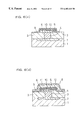
- FIG. 10 illustrates a common method for manufacturing a DRAM using a film with a high dielectric constant such as a BST film. Namely, first, as illustrated in FIG. 10 ( a ), after forming an n-type diffusion layer area 2 on, for instance, a p-type silicon substrate 1 through an ion implantation method, an oxide film is deposited through, for instance, the CVD (chemical vapor-phase epitaxy) method to form a layer insulating film 3 . Next, by employing the photolithography method and dry etching technology, a contact hole passing through to the n-type diffusion layer 2 is formed, and following this step, a polycrystal silicon plug 4 is formed by doping phosphorus within the contact hole.
- CVD chemical vapor-phase epitaxy
- a capacitor upper electrode e.g., Ru 8 is formed through sputtering, thereby completing the production of the memory capacitor portion of the DRAM, as illustrated in FIG. 10 ( c ).
- contact holes which pass through to the n-type diffusion areas are formed at the layer insulating film 36 , and a polycrystal silicon film 37 is formed inside a contact hole and an impurity such as phosphorus is added.
- a tungsten silicide film is deposited and a bit line 38 is formed by adopting the photolithography and etching technologies.
- an oxide film is deposited through the CVD method to form a layer insulating film 39 , and then a polycrystal silicon film 40 containing arsenic is formed inside a contact hole and on the layer insulating film 39 and the polycrystal silicon film 40 is made to fill inside the contact hole.
- the lattice constant of the oxide having such a perovskite crystal structure is very close to the lattice constant of the BST film which also has a perovskite crystal structure, their crystal lattices can achieve a better match when the BST film is formed on the perovskite oxide electrode, which makes it possible to maintain a good state for the interface between the BST film and the electrode.
- An even better interface condition can be achieved by improving the matching of the crystal lattices through the use of a single crystal BST film without any torsion in the lattice.
- Japanese Unexamined Patent Publication No. 1997-82915 presents a problem in that since the elements constituting the BST film and the ruthenium electrode are made to solid dissolve only through a mutual diffusion achieved by the heat treatment, the heat treatment must be implemented at a high temperature of approximately 700 centigrade in an oxygen atmosphere, which results in the ruthenium electrode and the barrier metal (e.g., TiN) formed under the ruthenium electrode becoming oxidized to an excessive degree. This causes the conductivity of the electrode to become degraded, to reduce the apparent dielectric constant of the dielectric substance.
- the barrier metal e.g., TiN
- a transitional layer with an inconsistent composition is formed if the elements are caused to dissolve only through a mutual diffusion effected by the heat treatment.
- titanium oxide (TiO 2 ) with a low dielectric constant will be formed in the transitional layer area having a composition with high Ti content, to reduce the apparent dielectric constant of the dielectric substance.
- BaCl 2 and SrCl 2 produced as a result of etching conductive materials such as BaRuO 3 and SrRuO 3 have extremely high melting points of 963 centigrade and 875 centigrade respectively, to present great difficulty in processing through the dry etching technology.
- An object of the present invention which has been completed by addressing the problems of the prior art discussed above, is to provide a new and improved method for manufacturing a semiconductor device through which a capacitor structure using a very thin dielectric film with a high dielectric constant can be manufactured with ease and at low cost by forming a transitional layer with a consistent composition at an interface of a ruthenium-type electrode and a dielectric substance having a perovskite structure with a high degree of efficiency.
- a method for manufacturing a semiconductor device achieved by laminating a plurality of conductive electrodes constituted of at least one type of material selected from a group of high melting point noble metals comprising platinum, iridium and ruthenium, and a dielectric film constituted of a film with a high dielectric constant, e.g., a dielectric film having a perovskite structure, that comprises a step in which a first conductive electrode is formed, a step in which a first area where elements constituting the first conductive electrode and elements constituting a first dielectric film are melded is formed, a step in which a transitional layer is formed by performing a heat treatment on the first area where the elements are melded and a step in which the first dielectric film is formed on the first conductive electrode, is provided.
- a good transitional layer constituted of an oxide layer (Ba X Sr Y Ru Z Ti W O 3 layer) can be achieved simply through the mutual diffusion effected by a heat treatment performed at a relatively low temperature.
- this transitional layer is formed on the lower electrode while aligning itself on the lower electrode, the lower electrode, which corresponds to the SrRuO 3 layer in the prior art can be formed easily.
- the dry etching step which is required in the method in the prior art, can be omitted to achieve simplification in the manufacturing process which, in turn, will reduce the production costs and improve the yield.
- the sputtering quantities for the individual elements constituting the dielectric film, which is driven into the lower electrode can be varied in correspondence to the power of the high-frequency voltage applied to the semiconductor substrate by, for instance, forming the meld area while applying a high-frequency voltage to the semiconductor substrate where the conductive electrode is formed and forming a dielectric layer on the conductive electrode, control over the composition of the meld area is achieved.
- a fully oxidized transitional layer can be formed by, for instance, forming the meld area within an oxidizing atmosphere in which the oxygen concentration within the gas composition is increased so that the oxygen content in the meld area can be increased.
- a conductive oxide film which is an oxide of the lower electrode (e.g., Ru) can be formed at the front surface of the lower electrode and, as a result, the oxygen content in the meld area can be increased by achieving a fully oxidized transitional layer.
- the elements constituting the dielectric film can be melded into the surface of the lower electrode in great quantities with better control compared to the method in which a high-frequency voltage is applied to the semiconductor substrate.
- transitional layer through a heat treatment performed in a non-oxidizing atmosphere, excessive oxidation does not occur at the lower electrode and the barrier metal so that a good transitional layer constituted of an oxide layer (Ba X Sr Y Ru Z Ti W O 3 layer) is achieved. Furthermore, if the heat treatment is performed at a low temperature of 500 centigrade or lower, a good transitional layer is formed since the lower electrode will not be oxidized even within the oxidizing atmosphere.
- a good interface is formed between the upper electrode and the dielectric film in addition to the interface between the lower electrode and the dielectric film.
- the sputtering quantities for the individual elements constituting the electrode that is driven into the second dielectric film can be varied in correspondence to the power of the high-frequency voltage applied to the semiconductor substrate, to achieve control over the composition of the meld area.
- this step in an oxidizing atmosphere with a higher oxygen concentration within the gas composition, the oxygen content in a specific meld area corresponding to the electrode film initial layer can be increased by achieving a more oxidized transitional layer.
- the elements constituting the upper electrode can be melded into the surface of the dielectric film through the ion implantation technology and, as a result, compared to the method in which a high-frequency voltage is applied to the semiconductor substrate, the elements constituting the upper electrode can be melded into the surface of the dielectric substance in great quantities with better control.
- FIG. 1 is a cross section illustrating the structure of a sputtering apparatus employed in the method for manufacturing a semiconductor device in an embodiment of the present invention
- FIGS. 2 ( a )- 2 ( d ) present schematic cross sections illustrating the process for manufacturing a DRAM in a first embodiment of the present invention
- FIG. 3 illustrates the relationship between the high-frequency voltage applied during the formation of the dielectric film and the reverse sputtering quantities of the individual elements in the first embodiment of the present invention
- FIGS. 8 ( a )- 8 ( c ) present schematic cross sections illustrating the process for manufacturing a DRAM in a fifth embodiment of the present invention
- an n-type diffusion area 2 is formed on, for instance, a p-type silicon substrate 1 through ion implantation, and then, a layer insulating film 3 having a film thickness of 100 nm ⁇ 1000 nm is formed through, for instance, the CVD method.
- a contact hole passing through to the n-type diffusion area 2 is formed and a polycrystal silicon plug 4 is formed by doping phosphorus inside the contact hole.
- a barrier metal film 5 e.g., TiN
- a ruthenium-type lower electrode film e.g, Ru
- a structure in which the lower electrode 6 and the barrier metal 5 are connected with the diffusion layer 2 formed on the silicon substrate 1 via the silicon plug 4 is completed. It is to be noted that this is similar to the manufacturing methods in the prior art.
- a high-frequency voltage is applied by the high frequency source 20 to the silicon substrate 1 on which the treatment described above has been performed to form a dielectric initial layer (e.g., BST layer) 9 having a film thickness of 10 nm and a perovskite structure on the lower electrode 6 and the layer insulating film 3 exposed at the surface of the silicon substrate 1 by adopting film formation technologies such as sputtering and the CVD method.
- a dielectric initial layer e.g., BST layer
- the dielectric initial layer 9 When the dielectric initial layer 9 is formed by applying a high-frequency voltage to the silicon substrate in this manner, a voltage that is negative relative to the plasma potential is applied to the silicon substrate 1 . As a result, Ar ions and O ions enter the silicon substrate 1 , and further, Ba ions, Sr ions and Ti ions which are the elements constituting the dielectric initial layer 9 enter the silicon substrate 1 . This, in turn, causes the dielectric initial layer 9 and the lower electrode 6 deposited on the silicon substrate 1 to become reverse sputtered, the Ba ions, the Sr ions and the Ti ions of the elements constituting the dielectric initial layer 9 are driven into the lower electrode 6 . Thus, a state in which the elements constituting the dielectric initial layer 9 are melded is achieved at the surface of the lower electrode 6 .
- FIG. 5 presents the relative dielectric constants of the dielectric initial layer (BST layer) 9 formed by adopting the method in this embodiment, of a BST layer formed through a common film formation method and of a BST layer formed by adopting the method in which a transitional layer is formed through a heat treatment (Japanese Unexamined Patent Publication No. 1997-82915).
- the BST layer formed through the method in this embodiment of the present invention achieves the highest dielectric constant.
- a heat treatment is performed on the dielectric initial layer (BST layer) 9 at a temperature within the range of 300 ⁇ 700 centigrade in a non-oxidizing atmosphere (e.g. N 2 ).
- a non-oxidizing atmosphere e.g. N 2
- a transitional layer 10 is formed between the dielectric initial layer 9 and the lower electrode 6 even through the heat treatment has been performed at low temperature, to achieve a good interface state.
- the heat treatment may be implemented either in a heat treatment furnace or through rapid heating, it is more desirable to perform the heat treatment through rapid heating considering its advantage of preventing oxygen from becoming diffused to an excessive degree.
- a second dielectric film e.g., a BST film 11 having a film thickness of 40 nm and a perovskite structure is formed through the film formation technologies such as sputtering and the CVD method.
- a ruthenium-type upper electrode e.g., Ru
- wiring, a passivation film and the like are formed through normal LSI processes to complete the DRAM product.
- a second dielectric film e.g., a BST film 11 having a film thickness of 40 nm and a perovskite structure is formed by adopting the film formation technologies such as sputtering and the CVD method.
- a ruthenium-type upper electrode (e.g. Ru) 8 having a film thickness of 50 nm ⁇ 300 nm is formed through sputtering to complete the DRAM capacitor structure.
- wiring, a passivation film and the like are formed through normal LSI processes to complete the DRAM product.
- the manufacturing method in the prior art is adopted up to the step in which a capacitor ruthenium-type lower electrode 6 and a barrier metal 5 are formed after forming a contact hole in the n-type diffusion area 2 and a polycrystal silicon plug 4 within the contact hole by doping with phosphorus, as in the first embodiment.
- a high-frequency voltage is applied to the silicon substrate 1 while forming the upper electrode initial layer 13 to cause Ar ions and O ions to enter the silicon substrate 1 and cause the elements constituting the dielectric film (Ba, Sr, Ti) to become melded into the upper electrode initial layer 13 .
- the transitional layer 14 is formed between the second dielectric film 11 and the second upper electrode 15 even though the heat treatment is performed at a low temperature and in a non-oxidizing atmosphere, resulting in an improved state of the interface of the second dielectric film 13 and the second upper electrode 15 . Consequently, in addition to the improvement in the state of the interface of the dielectric initial layer 9 and the lower electrode 6 , an improvement is achieved in the state of the interface between the second dielectric film 11 and the second upper electrode 15 , to further improve the dielectric film characteristics.
- a heat treatment is performed at a temperature within the range of 300 ⁇ 700 centigrade in a non-oxidizing atmosphere (e.g., N 2 ).
- the elements constituting the second upper electrode film 15 can be melded into the surface of the second dielectric film 11 by melding the element constituting the second upper electrode film 15 at the surface of the second dielectric film 11 through the ion implantation technology.
- the elements constituting the second upper electrode film 15 can be melded into the surface of the second dielectric film 11 in great quantities with better control compared to the method in which a high-frequency voltage is applied to the silicon substrate 1 , as in the fifth embodiment.
- the present invention is not restricted to this example, and depending upon the characteristics of the interface of the electrode and the highly dielectric film and factors such as the film thickness of the oxide film formed on the electrode and the like, the heat treatment temperature, the atmosphere, the length of time and the like can be set as appropriate.
- the present invention is not restricted to this example, and as long as the lower electrode and the barrier metal are not oxidized, the present invention can be implemented by using another inert gas such as Ar, He, Ne or the like. Consequently, the present invention can be carried out even within an oxidizing atmosphere when performing the heat treatment on the meld area as long as the heat treatment is implemented at a low temperature of, for instance, 500 centigrade or lower.
- the present invention is not restricted to this example, and it may be implemented by performing a batch heat treatment after forming the meld area and the capacitor structure.
- the present invention is not restricted to this example, and the present invention can be implemented by using a dielectric film material with a high dielectric constant which contains an alkaline earth metal such as SrTiO 3 , BaTiO 3 , Pb(Zr, Ti)O 3 , SrBi 2 TiO 3 or the like as a main constituent.
- the present invention may be implemented by using a dielectric film constituted of Ta 2 O 5 or the like instead of a dielectric material having a perovskite structure.
- the present invention is not restricted to this example and the present invention may be implemented by employing the deposition method, the MBE method, the sol-gel method, the laser ablation method or the like.
- ruthenium is used as an electrode material
- the present invention is not restricted to this example, and it may be implemented by using a conductive material containing a precious metal having a high melting point such as iridium (Ir), platinum (Pt) or the like as an electrode material or by using a compound such as titanium nitride (TiN), tungsten nitride (WN) or the like as an electrode material.
- a conductive material containing a precious metal having a high melting point such as iridium (Ir), platinum (Pt) or the like
- TiN titanium nitride
- WN tungsten nitride
- the present invention is not restricted to this example and it may be implemented by varying conditions such as the high-frequency voltage to be applied to the substrate and the conditions of the heat treatment in correspondence to the film thicknesses of the individual dielectric substances and the film thicknesses of the individual electrodes.
- the present invention is not restricted to this example, and it may be carried out in any semiconductor device as long as it has a capacitor structure that employs a highly dielectric film as an insulating film, such as an FRAM.
- a transitional layer (Ba X Sr Y Ru Z Ti W O 3 layer) can be formed between the dielectric film having a perovskite structure and the ruthenium-type electrode through heat treatment performed within a non-oxidizing atmosphere at a low temperature, the lower electrode and the barrier metal do not become oxidized to an excessive degree, so that a good interface is achieved between the dielectric film and the electrode. As a result, even when an extremely thin, highly dielectric film is used, the leak current flowing from the dielectric film is reduced to achieve good dielectric film characteristics.
- the transitional layer can be formed on the lower electrode through self alignment by performing a heat treatment on the meld area formed in the lower electrode, the lower electrode can be formed easily without having to dry etch the transitional layer. As a result, the step for dry etching the transitional layer can be omitted to simplify the manufacturing process which, in turn, will reduce the production costs and improve the yield.
Abstract
Description
Claims (13)
Applications Claiming Priority (2)
| Application Number | Priority Date | Filing Date | Title |
|---|---|---|---|
| JP10183692A JP2000022105A (en) | 1998-06-30 | 1998-06-30 | Manufacture of semiconductor device |
| JP10-183692 | 1998-06-30 |
Publications (1)
| Publication Number | Publication Date |
|---|---|
| US6403441B1 true US6403441B1 (en) | 2002-06-11 |
Family
ID=16140279
Family Applications (1)
| Application Number | Title | Priority Date | Filing Date |
|---|---|---|---|
| US09/291,306 Expired - Lifetime US6403441B1 (en) | 1998-06-30 | 1999-04-15 | Method for fabricating storage capacitor using high dielectric constant material |
Country Status (2)
| Country | Link |
|---|---|
| US (1) | US6403441B1 (en) |
| JP (1) | JP2000022105A (en) |
Cited By (8)
| Publication number | Priority date | Publication date | Assignee | Title |
|---|---|---|---|---|
| US20020017723A1 (en) * | 1999-06-03 | 2002-02-14 | Oki Electric Industry Co., Ltd. | Semiconductor memory device and method for the manufacture thereof |
| US20020021544A1 (en) * | 2000-08-11 | 2002-02-21 | Hag-Ju Cho | Integrated circuit devices having dielectric regions protected with multi-layer insulation structures and methods of fabricating same |
| US6472319B2 (en) * | 2000-12-19 | 2002-10-29 | Samsung Electronics Co., Ltd. | Method for manufacturing capacitor of semiconductor memory device by two-step thermal treatment |
| US20030045022A1 (en) * | 2001-08-30 | 2003-03-06 | Eldridge Jerome Michael | Perovskite-type material forming methods, capacitor dielectric forming methods, and capacitor constructions |
| US20040036571A1 (en) * | 2002-03-15 | 2004-02-26 | I-Wei Chen | Magnetically-and electrically-induced variable resistance materials and method for preparing same |
| US20040097034A1 (en) * | 2000-06-07 | 2004-05-20 | Sandhu Gurtej S. | Capacitor structure |
| US20040175492A1 (en) * | 1999-12-23 | 2004-09-09 | Won Seok-Jun | Methods of forming ruthenium film by changing process conditions during chemical vapor deposition and ruthenium films formed thereby |
| US11424316B2 (en) | 2019-12-13 | 2022-08-23 | Samsung Electronics Co., Ltd. | Capacitor structure and semiconductor device including the same |
Families Citing this family (3)
| Publication number | Priority date | Publication date | Assignee | Title |
|---|---|---|---|---|
| US6562678B1 (en) * | 2000-03-07 | 2003-05-13 | Symetrix Corporation | Chemical vapor deposition process for fabricating layered superlattice materials |
| US6762090B2 (en) | 2001-09-13 | 2004-07-13 | Hynix Semiconductor Inc. | Method for fabricating a capacitor |
| JP4882457B2 (en) * | 2006-03-31 | 2012-02-22 | 富士通株式会社 | Thin film capacitor and semiconductor device having the same |
Citations (9)
| Publication number | Priority date | Publication date | Assignee | Title |
|---|---|---|---|---|
| US3972059A (en) * | 1973-12-28 | 1976-07-27 | International Business Machines Corporation | Dielectric diode, fabrication thereof, and charge store memory therewith |
| JPH0786514A (en) | 1993-09-13 | 1995-03-31 | Nec Corp | Thin film capacitor |
| JPH0982915A (en) | 1995-09-18 | 1997-03-28 | Toshiba Corp | Manufacture of semiconductor device |
| JPH09246490A (en) | 1996-03-11 | 1997-09-19 | Toshiba Corp | Semiconductor device and manufacture thereof |
| US5789268A (en) * | 1995-10-31 | 1998-08-04 | Northern Telecom Limited | Method of forming a electrode structure for ferroelectric capacitors for integrated circuits |
| US5807774A (en) | 1996-12-06 | 1998-09-15 | Sharp Kabushiki Kaisha | Simple method of fabricating ferroelectric capacitors |
| US6010744A (en) * | 1997-12-23 | 2000-01-04 | Advanced Technology Materials, Inc. | Method for nucleation controlled chemical vapor deposition of metal oxide ferroelectric thin films |
| US6025257A (en) * | 1996-03-13 | 2000-02-15 | Lg Semicon Co., Ltd. | Method for preparing dielectric thin film and semiconductor device using same |
| US6078072A (en) * | 1997-10-01 | 2000-06-20 | Mitsubishi Denki Kabushiki Kaisha | Semiconductor device having a capacitor |
-
1998
- 1998-06-30 JP JP10183692A patent/JP2000022105A/en active Pending
-
1999
- 1999-04-15 US US09/291,306 patent/US6403441B1/en not_active Expired - Lifetime
Patent Citations (9)
| Publication number | Priority date | Publication date | Assignee | Title |
|---|---|---|---|---|
| US3972059A (en) * | 1973-12-28 | 1976-07-27 | International Business Machines Corporation | Dielectric diode, fabrication thereof, and charge store memory therewith |
| JPH0786514A (en) | 1993-09-13 | 1995-03-31 | Nec Corp | Thin film capacitor |
| JPH0982915A (en) | 1995-09-18 | 1997-03-28 | Toshiba Corp | Manufacture of semiconductor device |
| US5789268A (en) * | 1995-10-31 | 1998-08-04 | Northern Telecom Limited | Method of forming a electrode structure for ferroelectric capacitors for integrated circuits |
| JPH09246490A (en) | 1996-03-11 | 1997-09-19 | Toshiba Corp | Semiconductor device and manufacture thereof |
| US6025257A (en) * | 1996-03-13 | 2000-02-15 | Lg Semicon Co., Ltd. | Method for preparing dielectric thin film and semiconductor device using same |
| US5807774A (en) | 1996-12-06 | 1998-09-15 | Sharp Kabushiki Kaisha | Simple method of fabricating ferroelectric capacitors |
| US6078072A (en) * | 1997-10-01 | 2000-06-20 | Mitsubishi Denki Kabushiki Kaisha | Semiconductor device having a capacitor |
| US6010744A (en) * | 1997-12-23 | 2000-01-04 | Advanced Technology Materials, Inc. | Method for nucleation controlled chemical vapor deposition of metal oxide ferroelectric thin films |
Non-Patent Citations (2)
| Title |
|---|
| Mitsuaki Izuha et al., "Electrical Properties of All-Perovskite Oxide (SrRuO3/BaxSr1-xTiO3/SrRuO3)," Jpn. J. Appl. Phys. vol. 36 (1997) pp. 5866-5869, Part 1, No. 9B, Sep. 1997. |
| Wolf et al. Silicon Processing for the VLSI Era, vol. 1, Lattice Press: Sunset Beach, CA, 1986, pp. 357-361.* * |
Cited By (23)
| Publication number | Priority date | Publication date | Assignee | Title |
|---|---|---|---|---|
| US6710384B2 (en) * | 1999-06-03 | 2004-03-23 | Oki Electric Industry Co., Ltd. | Semiconductor memory device |
| US20020017723A1 (en) * | 1999-06-03 | 2002-02-14 | Oki Electric Industry Co., Ltd. | Semiconductor memory device and method for the manufacture thereof |
| US20040175492A1 (en) * | 1999-12-23 | 2004-09-09 | Won Seok-Jun | Methods of forming ruthenium film by changing process conditions during chemical vapor deposition and ruthenium films formed thereby |
| US7271038B2 (en) * | 1999-12-23 | 2007-09-18 | Samsung Electronics Co., Ltd. | Methods of forming ruthenium film by changing process conditions during chemical vapor deposition and ruthenium films formed thereby |
| US20080017950A1 (en) * | 1999-12-23 | 2008-01-24 | Samsung Electronics, Co., Ltd. | Methods of forming ruthenium film by changing process conditions during chemical vapor deposition and ruthenium films formed thereby |
| US20040097034A1 (en) * | 2000-06-07 | 2004-05-20 | Sandhu Gurtej S. | Capacitor structure |
| US20060258113A1 (en) * | 2000-06-07 | 2006-11-16 | Micron Technology, Inc. | Capacitor structure |
| US8421140B2 (en) * | 2000-06-07 | 2013-04-16 | Micron Technology, Inc. | Dielectric structures |
| US7023037B2 (en) | 2000-08-11 | 2006-04-04 | Samsung Electronics Co., Ltd. | Integrated circuit devices having dielectric regions protected with multi-layer insulation structures |
| US6740531B2 (en) * | 2000-08-11 | 2004-05-25 | Samsung Electronics Co., Ltd. | Method of fabricating integrated circuit devices having dielectric regions protected with multi-layer insulation structures |
| US20020021544A1 (en) * | 2000-08-11 | 2002-02-21 | Hag-Ju Cho | Integrated circuit devices having dielectric regions protected with multi-layer insulation structures and methods of fabricating same |
| US20040183116A1 (en) * | 2000-08-11 | 2004-09-23 | Hag-Ju Cho | Integrated circuit devices having dielectric regions protected with multi-layer insulation structures and methods of fabricating same |
| US6472319B2 (en) * | 2000-12-19 | 2002-10-29 | Samsung Electronics Co., Ltd. | Method for manufacturing capacitor of semiconductor memory device by two-step thermal treatment |
| US20030045022A1 (en) * | 2001-08-30 | 2003-03-06 | Eldridge Jerome Michael | Perovskite-type material forming methods, capacitor dielectric forming methods, and capacitor constructions |
| US6730575B2 (en) * | 2001-08-30 | 2004-05-04 | Micron Technology, Inc. | Methods of forming perovskite-type material and capacitor dielectric having perovskite-type crystalline structure |
| US6908827B2 (en) | 2001-08-30 | 2005-06-21 | Micron Technology, Inc. | Perovskite-type material forming methods, capacitor dielectric forming methods, and capacitor constructions |
| US6897513B2 (en) | 2001-08-30 | 2005-05-24 | Micron Technology, Inc. | Perovskite-type material forming methods, capacitor dielectric forming methods, and capacitor constructions |
| US20040092107A1 (en) * | 2001-08-30 | 2004-05-13 | Eldridge Jerome M. | Perovskite-type material forming methods, capacitor dielectric forming methods, and capacitor constructions |
| US7211199B2 (en) * | 2002-03-15 | 2007-05-01 | The Trustees Of The University Of Pennsylvania | Magnetically-and electrically-induced variable resistance materials and method for preparing same |
| US20040036571A1 (en) * | 2002-03-15 | 2004-02-26 | I-Wei Chen | Magnetically-and electrically-induced variable resistance materials and method for preparing same |
| US20080174400A1 (en) * | 2003-03-17 | 2008-07-24 | The Trustees Of The University Of Pennsylvania | Magnetically-and electrically-induced variable resistance materials and method for preparing same |
| US8652347B2 (en) * | 2003-03-17 | 2014-02-18 | The Trustees Of The University Of Pennsylvania | Magnetically-and electrically-induced variable resistance materials and method for preparing same |
| US11424316B2 (en) | 2019-12-13 | 2022-08-23 | Samsung Electronics Co., Ltd. | Capacitor structure and semiconductor device including the same |
Also Published As
| Publication number | Publication date |
|---|---|
| JP2000022105A (en) | 2000-01-21 |
Similar Documents
| Publication | Publication Date | Title |
|---|---|---|
| US5736449A (en) | Semiconductor memory device having improved isolation between electrodes, and process for fabricating the same | |
| JP3319994B2 (en) | Semiconductor storage element | |
| US6180974B1 (en) | Semiconductor storage device having a capacitor electrode formed of at least a platinum-rhodium oxide | |
| US6483143B2 (en) | Semiconductor device having a capacitor structure including a self-alignment deposition preventing film | |
| US6335551B2 (en) | Thin film capacitor having an improved bottom electrode and method of forming the same | |
| US20060199311A1 (en) | Antifuse having tantalum oxynitride film and method for making same | |
| US20060258113A1 (en) | Capacitor structure | |
| JPH09116115A (en) | Manufacture of capacitor for semiconductor element | |
| KR19990013720A (en) | Ferroelectric Capacitor, Manufacturing Method Thereof and Memory Cell Using the Capacitor | |
| US6403441B1 (en) | Method for fabricating storage capacitor using high dielectric constant material | |
| US20060154382A1 (en) | Capacitor with high dielectric constant materials and method of making | |
| KR101084408B1 (en) | Semiconductor device and process for producing the semiconductor device | |
| US6828190B2 (en) | Method for manufacturing capacitor of semiconductor device having dielectric layer of high dielectric constant | |
| JPH1056145A (en) | Method for manufacturing semiconductor integrated circuit device | |
| KR100382719B1 (en) | Semiconductor device comprising ferroelectric capacitor and method of manufacturing the same | |
| JP3931113B2 (en) | Semiconductor device and manufacturing method thereof | |
| JPH08335682A (en) | Electron device manufacture | |
| US6297085B1 (en) | Method for manufacturing ferroelectric capacitor and method for manufacturing ferroelectric memory | |
| US20020125524A1 (en) | Semiconductor device and method of manufacturing same | |
| JP3638518B2 (en) | Structured metal oxide-containing layer and method for producing semiconductor structure element | |
| US6670668B2 (en) | Microelectronic structure, method for fabricating it and its use in a memory cell | |
| US20030175425A1 (en) | Vapor phase deposition method for metal oxide dielectric film | |
| US6504228B1 (en) | Semiconductor device and method for manufacturing the same | |
| JP2000195956A (en) | Method of forming lower electrode of capacitor | |
| JP2000503725A (en) | Method for producing dielectric layer or ferroelectric layer having high dielectric constant ε |
Legal Events
| Date | Code | Title | Description |
|---|---|---|---|
| AS | Assignment |
Owner name: OKI ELECTRIC INDUSTRY CO., LTD., JAPAN Free format text: ASSIGNMENT OF ASSIGNORS INTEREST;ASSIGNORS:TAKEHIRO, SHINOBU;YOSHIMARU, MASAKI;REEL/FRAME:009903/0179 Effective date: 19990406 |
|
| STCF | Information on status: patent grant |
Free format text: PATENTED CASE |
|
| FPAY | Fee payment |
Year of fee payment: 4 |
|
| AS | Assignment |
Owner name: OKI SEMICONDUCTOR CO., LTD., JAPAN Free format text: CHANGE OF NAME;ASSIGNOR:OKI ELECTRIC INDUSTRY CO., LTD.;REEL/FRAME:022343/0290 Effective date: 20081001 |
|
| FPAY | Fee payment |
Year of fee payment: 8 |
|
| FPAY | Fee payment |
Year of fee payment: 12 |
|
| AS | Assignment |
Owner name: LAPIS SEMICONDUCTOR CO., LTD., JAPAN Free format text: CHANGE OF NAME;ASSIGNOR:OKI SEMICONDUCTOR CO., LTD;REEL/FRAME:032495/0483 Effective date: 20111003 |