EP0566187B1 - Verfahren zur Herstellung einer nichtflüchtigen grabenförmigen Speicheranordnung - Google Patents
Verfahren zur Herstellung einer nichtflüchtigen grabenförmigen Speicheranordnung Download PDFInfo
- Publication number
- EP0566187B1 EP0566187B1 EP93201004A EP93201004A EP0566187B1 EP 0566187 B1 EP0566187 B1 EP 0566187B1 EP 93201004 A EP93201004 A EP 93201004A EP 93201004 A EP93201004 A EP 93201004A EP 0566187 B1 EP0566187 B1 EP 0566187B1
- Authority
- EP
- European Patent Office
- Prior art keywords
- mesas
- oxide
- layer
- forming
- memory device
- Prior art date
- Legal status (The legal status is an assumption and is not a legal conclusion. Google has not performed a legal analysis and makes no representation as to the accuracy of the status listed.)
- Expired - Lifetime
Links
Images
Classifications
-
- H—ELECTRICITY
- H10—SEMICONDUCTOR DEVICES; ELECTRIC SOLID-STATE DEVICES NOT OTHERWISE PROVIDED FOR
- H10B—ELECTRONIC MEMORY DEVICES
- H10B41/00—Electrically erasable-and-programmable ROM [EEPROM] devices comprising floating gates
- H10B41/20—Electrically erasable-and-programmable ROM [EEPROM] devices comprising floating gates characterised by three-dimensional arrangements, e.g. with cells on different height levels
- H10B41/23—Electrically erasable-and-programmable ROM [EEPROM] devices comprising floating gates characterised by three-dimensional arrangements, e.g. with cells on different height levels with source and drain on different levels, e.g. with sloping channels
- H10B41/27—Electrically erasable-and-programmable ROM [EEPROM] devices comprising floating gates characterised by three-dimensional arrangements, e.g. with cells on different height levels with source and drain on different levels, e.g. with sloping channels the channels comprising vertical portions, e.g. U-shaped channels
-
- H—ELECTRICITY
- H10—SEMICONDUCTOR DEVICES; ELECTRIC SOLID-STATE DEVICES NOT OTHERWISE PROVIDED FOR
- H10B—ELECTRONIC MEMORY DEVICES
- H10B69/00—Erasable-and-programmable ROM [EPROM] devices not provided for in groups H10B41/00 - H10B63/00, e.g. ultraviolet erasable-and-programmable ROM [UVEPROM] devices
Definitions
- the invention is in the field of methods of making nonvolatile trench memories, and relates specifically to memory devices such as Electrically Erasable and Programmable Read Only Memory (EEPROM) Devices.
- EEPROM Electrically Erasable and Programmable Read Only Memory
- EEPROM devices in general, and methods for making such devices are well known in the art. Some typical prior-art memory devices and methods are shown and discussed in Patent Abstracts of Japan: Vol. 13, No. 548 (E-856) (3896)JP-A1-227.477; Vol. 13 No. 198 (E-756) (3546), JP-A1-20.668; Vol. 12 No. 153 (E-607) (3000), JP-A 62-269363; Vol. 11 No. 108 (E-495) (2555), JP-A 61-256673; Vol. 15 No. 108 (E-1045) (4636), JP-A 3-1574.
- Patent Abstracts of Japanese Kokai No. 1-20668 is directed to improved density and size reduction in PROM devices. Nevertheless, in that reference, a complex structure is employed in which the word line clearly overlaps the trench, and in which the drain contact metallization must be laterally isolated from surrounding parts of the device by separate insulation regions. Both of these features increase the size and complexity of the resuiting device.
- the smallest known EEPROM cell has a cell area of 3.6 microns 2 .
- the trench memory cell configuration lends itself to further size reduction because the channel can be stretched in the vertical direction to avoid operational problems without increasing device area, the potential advantages of this device configuration have not heretofore been fully realized due to conventional lithography alignment tolerances and space-consuming draincontact metallization configurations.
- Yet another object of the invention is to provide a simple, efficient and economical method for manufacturing highly-compact nonvolatile trench memory devices as EEPROMs.
- a nonvolatile trench memory device in accordance with the invention is fabricated using a unique self-aligned method which permits an extremely compact and simple device configuration.
- a method according to the invention of making a nonvolatile trench memory device comprises:
- the advantageous features of the present invention are achieved by a process in which polysilicon mesas are formed integrally with the control gates, with the mesas extending above the surface of the body region and extending between trenches in which the memory devices are formed so as to form the word lines of the memory device.
- the top and sides of these mesas are then oxidized to create a capping insulating layer that isolates the word lines without taking up any additional space in the lateral direction.
- Bit lines can then be formed in a direction perpendicular to that of the word lines, and can contact drain regions of the device and extend directly over the oxide-capped word lines without the necessity for any addition bit-line isolation regions in the lateral direction. Due to the extensive use of self-aligned process techniques, extremely tight tolerances can be maintained without regard for lithographic tolerances, and the end result is an extremely compact, simple and easy to manufacture device.
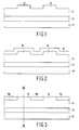
- Figs. 1-9 show a nonvolatile trench memory device in successive stages of manufacture, in accordance with the invention.
- Figs. 1-3 of the drawing show three early stages of the manufacture a nonvolatile trench memory device in accordance with the invention.
- the starting material may typically be an n++ substrate 10 having a doping level of about 10 21 atom/cm 3 .
- the substrate will ultimately form a low-resistance common source of the memory.
- n-type epitaxial layer 12 having a thickness of about 3.0 microns and a doping concentration of about 10 16 atoms/cm 3 is formed on the substrate, and a p-type body region 14 having a thickness of about 1.7 microns and a surface concentration of about 10 17 atoms/cm 3 is formed on the epitaxial layer 12 by doping into the epitaxial layer.
- spaced-apart mesas 16 are formed which extent parallel to each other in a direction perpendicular to the view shown in Fig. 1.
- the thickness of these mesas is about 0.5 micron, so that the thickness of portions of the body region 14 located between the mesas 16 is about 1.2 microns.
- the oxidized surface of the body region 14 is then planarized down to the level of the mesas 16 to achieve a substantially flat surface 20 having alternating oxide stripes (18a, 18b, 18c) and mesas (16) which extent parallel to each other in a direction perpendicular to the view shown in Fig. 3.
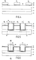
- a thin pad oxide 22, of about 0.03 microns thickness is formed on surface 20.
- a silicon nitride layer 24 which is about 0.1 microns thick is formed on pad oxide 22 and a thick LTO (low temperature oxide) layer 26 which is about 1 micron thick is deposited on the nitride layer 24.
- this triple layer 22, 24, 26 is then formed into a plurality of spaced-apart second mesas 28 on the surface 20 which extent parallel to each other in a direction perpendicular to that of the oxide stripes 18a, 18b, and 18c.
- the device viewed from above, has a series of first mesas 16 extending as stripes in a first direction between oxide stripes 18a, 18b, and 18c, as shown in Fig. 3, with a series of spaced-apart second mesas 28 extending parallel to each other in a direction perpendicular to that of the first mesas, as shown in Fig. 4.
- This structure forms a lattice configuration, when viewed from above, with square or rectangular portions of first mesas 16 being defined on a first pair of sides by oxide stripes 18a, 18b, 18c, and on a second pair of sides by the second mesas 28.
- the exposed rectangular or square portions of the first mesas 16 are then etched, using the oxide lattice as a mask, until trenches 30 which extend down through body region 14 and into epitaxial layer 12 are formed. These trenches, viewed from above, will have a square or rectangular shape, as defined by the oxide lattice.
- a thin gate dielectric layer 34 typically an oxide layer having a thickness of about 0.01-0.02 microns, on the side walls and bottom of the trenches 30.
- a polysilicon floating gate electrode 36 typically 0.1 microns thick, is then formed on the gate oxide 34, and is covered with an inter-gate dielectric 38, which may typically be an ONO (oxide, nitride, oxide) layer of about 0.03 microns thickness.
- the remaining open portion of the trench is then filled with a polysilicon control gate electrode 40, with the polysilicon gate electrodes being planarized at the level of the upper surface of the second mesas 28 to create a flat upper surface at this stage of the process, as shown in Fig. 5.
- the polysilicon which forms the gate electrodes extends not only into the trenches 30, as shown in Fig. 5, but also extends between memory cells 32 in a direction perpendicular to the view of Fig. 5, as shown by polysilicon portions 40a in Fig. 7 extending between the control gate electrodes 40.
- the top oxide layer 26 of the second mesas 28 is then selectively etched away down to the nitride layer 24, thus leaving the upper polysilicon portions of the gate electrodes above the level of the nitride layer 24 exposed.
- the exposed portions of the polysilicon gate electrodes above the level of nitride layer 24 are then thermally oxidized, using the nitride layer 24 as an oxidation mask, to form insulating oxide caps 42 on the top and sides of the exposed portions of polysilicon.
- the sidewall oxidation is self-limited because of the ONO between the floating gate polysilicon and the control gate polysilicon. This ensures that sufficient control gate polysilicon remains to permit conduction of word line signals.
- the resulting structure at this stage of the manufacturing process is shown in Fig. 6.
- Fig. 7 shows a cross-sectional view of the device along the section line VII-VII in Fig. 6.
- the polysilicon of the control gate electrodes 40 also has portions 40a which extend in the lateral direction between memory cells 32 to form word lines of the memory device. It can also be seen that the word lines are insulated from above by the insulating oxide cap 42, and from below by the oxide stripes 18a, 18b and 18c.
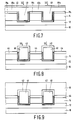
- These drain regions may typically be 0.4 microns thick and have a doping level of about 10 20 atoms/cm 3 .
- the drain regions may be formed by a number of different conventional techniques, such as ion implantation through the layers 22 and 24 (see Fig. 6), or by first removing the nitride layer 24 and then implanting through oxide layer 22.
- the drain regions part, or all (as shown), of the remaining portions of layers 22 and 24 are removed, by self-aligned contact formation, in which the nitride 24 is selectively removed by wet chemical etching, leaving the thin oxide layer 22. Since the thickness of oxide layer 22 is much less than that of the polysilicon oxide cap, oxide layer 22 can easily be removed, without exposing the polysilicon, to form a self-aligned contact to each drain. At least part of the drain regions 44 are exposed, as shown in Fig. 8.
- drain metallization lines 46 are then formed on the drain regions 44 and the insulating oxide caps 42, as shown in Fig. 9, in a third masking operation using conventional masking and etching techniques. These drain metallization lines extend in a direction perpendicular to the polysilicon word lines and thus form the bit lines of the memory device.
- the previously-described method yields an extremely compact, simple and easy to manufacture device. Whereas about 15 masks are typically needed to fabricate such a device using prior-art techniques, the method of the present invention permits the fabrication of a more compact device while requiring the use of only 3 masks, as described, plus an additional contact mask, thus resulting in substantially simplification while at the same time achieving superior results.
Claims (7)
- Verfahren zur Herstellung einer nichtflüchtigen, grabenförmigen Speicheranordnung, wonachein Halbleitersubstrat (10) eines ersten Leitfähigkeitstyps vorgesehen wird, welches eine gemeinsame Sourcezone der Anordnung bildet;eine epitaktische Schicht (12) des ersten Leitfähigkeitstyps auf dem Substrat ausgebildet wird;eine Körperzone (14) eines, mit diesem des ersten ungleichnamigen, zweiten Leitfähigkeitstyps auf der epitaktischen Schicht vorgesehen wird;mehrere, voneinander beabstandete, erste Mesas (16) auf einer Oberfläche der Körperzone ausgebildet werden, welche sich in einer ersten Richtung parallel zueinander erstrecken;eine Oxidschicht (18) auf der Oberfläche der Körperzone mit den ersten Mesas aufgebracht wird;die Oberfläche planarisiert wird, um eine im wesentlichen ebene Oberfläche mit Oxidstreifen (18a, 18b, 18c) vorzusehen, welche sich parallel zueinander und zwischen den ersten Mesas in der ersten Richtung erstrecken;mehrere, voneinander beabstandete, zweite Mesas (28) auf der ebenen Oberfläche ausgebildet werden, welche sich parallel zueinander in einer, im wesentlichen orthogonal zu der ersten Richtung verlaufenden, zweiten Richtung erstrecken, wobei die zweiten Mesas jeweils aus einer ersten, an die Oberfläche angrenzenden Schicht (22) aus Oxid, einer zweiten Schicht (24) aus Nitrid und einer dritten Schicht (26) aus Oxid vorgesehen werden;mehrere Gräben (30) in voneinander beabstandeten Abschnitten der Körperzone zwischen den ersten und den zweiten Mesas ausgebildet werden, wobei sich die Gräben zumindest durch die Körperzone zu der epitaktischen Schicht erstrecken;mehrere Speicherzellen (32) in den Gräben ausgebildet werden, wobei jede Speicherzelle durch konsekutive Ausbildung eines dünnen Gatedielektrikums (34) auf den Seitenwänden und dem Boden der Gräben, einer Floating-Gate-Elektrode (36) aus Polysilicium auf dem Gatedielektrikum vorgesehen und mit einer Zwischengate-Isolierschicht (38) abgedeckt, der verbleibende, freie Abschnitt sodann mit einer Steuergateelektrode (40) aus Polysilicium ausgefüllt wird, die Gateelektroden aus Polysilicium in Höhe der Oberfläche der zweiten Mesas planarisiert werden und sich das Polysilicium, zumindest der Steuergateelektroden, ebenfalls zwischen Speicherzellen in der zweiten Richtung erstreckt;die dritte Schicht (26) der zweiten Mesas so abgetragen wird, daß die oberen Polysiliciumabschnitte, zumindest der Steuergateelektroden, mehrere, voneinander beabstandete, dritte Mesas bilden, welche sich parallel zueinander in der zweiten Richtung erstrecken;die oberen Bereiche und Seiten der oberen Abschnitte aus Polysilicium einer Oxidation unterworfen werden, um eine Isolationsschicht (42) über den dritten Mesas und um diese herum vorzusehen, wobei die dritten Mesas isolierte Polysilicium-Wortleitungen der Speicheranordnung bilden;Drainzonen (44) des ersten Leitfähigkeitstyps in oberflächenangrenzenden Abschnitten der Körperzone zwischen den Oxidstreifen und den Speicherzellen ausgebildet werden;die erste und zweite Schicht (22, 24) der zweiten Mesas über den Drainzonen zumindest teilweise abgetragen werden; sowieDrainmetallisierungsleitungen (46) auf den Drainzonen und den oxidierten, oberen Abschnitte aus Polysilicium ausgebildet werden, wobei sich die Drainmetallisierungsleitungen zur Ausbildung von Bitleitungen der Speicheranordnung in der ersten Richtung erstrecken.
- Verfahren zur Herstellung einer nichtflüchtigen, grabenförmigen Speicheranordnung nach Anspruch 1, wobei die Oxidschicht auf der Oberfläche der Körperzone durch Oxidation der Oberfläche gebildet wird.
- Verfahren zur Herstellung einer nichtflüchtigen, grabenförmigen Speicheranordnung nach Anspruch 1, wobei die Oxidschicht auf der Oberfläche der Körperzone durch Aufbringen eines Niedertemperaturoxids auf der Oberfläche gebildet wird.
- Verfahren zur Herstellung einer nichtflüchtigen, grabenförmigen Speicheranordnung nach Anspruch 1, wobei die dritte Oxidschicht durch Aufbringen eines Niedertemperaturoxids gebildet wird.
- Verfahren zur Herstellung einer nichtflüchtigen, grabenförmigen Speicheranordnung nach Anspruch 1, wobei die Gräben durch rechteckige Gräben dargestellt sind.
- Verfahren zur Herstellung einer nichtflüchtigen, grabenförmigen Speicheranordnung nach Anspruch 1, wobei die Gräben durch quadratische Gräben dargestellt sind.
- Verfahren zur Herstellung einer nichtflüchtigen, grabenförmigen Speicheranordnung nach Anspruch 1, wobei das Zwischengate-Dielektrikum aus einer Oxid-Nitrid-Oxid-Schicht gebildet wird.
Applications Claiming Priority (2)
| Application Number | Priority Date | Filing Date | Title |
|---|---|---|---|
| US07/867,595 US5229312A (en) | 1992-04-13 | 1992-04-13 | Nonvolatile trench memory device and self-aligned method for making such a device |
| US867595 | 1992-04-13 |
Publications (3)
| Publication Number | Publication Date |
|---|---|
| EP0566187A2 EP0566187A2 (de) | 1993-10-20 |
| EP0566187A3 EP0566187A3 (de) | 1994-08-31 |
| EP0566187B1 true EP0566187B1 (de) | 1998-08-26 |
Family
ID=25350101
Family Applications (1)
| Application Number | Title | Priority Date | Filing Date |
|---|---|---|---|
| EP93201004A Expired - Lifetime EP0566187B1 (de) | 1992-04-13 | 1993-04-06 | Verfahren zur Herstellung einer nichtflüchtigen grabenförmigen Speicheranordnung |
Country Status (5)
| Country | Link |
|---|---|
| US (1) | US5229312A (de) |
| EP (1) | EP0566187B1 (de) |
| JP (1) | JP2545193B2 (de) |
| KR (1) | KR100281375B1 (de) |
| DE (1) | DE69320522T2 (de) |
Families Citing this family (21)
| Publication number | Priority date | Publication date | Assignee | Title |
|---|---|---|---|---|
| CN1040962C (zh) * | 1993-06-16 | 1998-12-02 | 日本写真印刷株式会社 | 印刷辊和印刷辊用弹性印版 |
| US20070004134A1 (en) * | 1996-05-29 | 2007-01-04 | Vora Madhukar B | Vertically integrated flash EPROM for greater density and lower cost |
| JPH1117034A (ja) * | 1997-06-24 | 1999-01-22 | Matsushita Electron Corp | 半導体記憶装置およびその製造方法 |
| US6013551A (en) * | 1997-09-26 | 2000-01-11 | Taiwan Semiconductor Manufacturing Company, Ltd. | Method of manufacture of self-aligned floating gate, flash memory cell and device manufactured thereby |
| US5854114A (en) * | 1997-10-09 | 1998-12-29 | Advanced Micro Devices, Inc. | Data retention of EEPROM cell with shallow trench isolation using thicker liner oxide |
| US6127226A (en) * | 1997-12-22 | 2000-10-03 | Taiwan Semiconductor Manufacturing Company | Method for forming vertical channel flash memory cell using P/N junction isolation |
| US6204123B1 (en) | 1998-10-30 | 2001-03-20 | Sony Corporation | Vertical floating gate transistor with epitaxial channel |
| US6870220B2 (en) * | 2002-08-23 | 2005-03-22 | Fairchild Semiconductor Corporation | Method and apparatus for improved MOS gating to reduce miller capacitance and switching losses |
| US6417048B1 (en) * | 2001-11-19 | 2002-07-09 | Vanguard International Semiconductor Corporation | Method for fabricating flash memory with recessed floating gates |
| US6661053B2 (en) | 2001-12-18 | 2003-12-09 | Infineon Technologies Ag | Memory cell with trench transistor |
| DE10162261B4 (de) * | 2001-12-18 | 2005-09-15 | Infineon Technologies Ag | Speicherzelle mit Grabentransistor |
| DE10229065A1 (de) * | 2002-06-28 | 2004-01-29 | Infineon Technologies Ag | Verfahren zur Herstellung eines NROM-Speicherzellenfeldes |
| DE10321742A1 (de) * | 2003-05-14 | 2004-12-09 | Infineon Technologies Ag | Integrierte Schaltungsanordnung mit Isoliergraben und Feldeffekttransistor sowie Herstellungsverfahren |
| JP2008171872A (ja) * | 2007-01-09 | 2008-07-24 | Elpida Memory Inc | 半導体装置及びその製造方法 |
| JP2009004510A (ja) * | 2007-06-20 | 2009-01-08 | Toshiba Corp | 不揮発性半導体記憶装置 |
| US8081515B2 (en) | 2008-04-04 | 2011-12-20 | Trom | Trench monos memory cell and array |
| US7915124B2 (en) * | 2008-07-09 | 2011-03-29 | Sandisk Corporation | Method of forming dielectric layer above floating gate for reducing leakage current |
| US7919809B2 (en) * | 2008-07-09 | 2011-04-05 | Sandisk Corporation | Dielectric layer above floating gate for reducing leakage current |
| US8207036B2 (en) * | 2008-09-30 | 2012-06-26 | Sandisk Technologies Inc. | Method for forming self-aligned dielectric cap above floating gate |
| JP5364128B2 (ja) * | 2011-05-30 | 2013-12-11 | 日油技研工業株式会社 | 滅菌インジケータの退色及び転写の抑制材、及びそれを用いた滅菌バッグ |
| TWI470790B (zh) * | 2012-07-13 | 2015-01-21 | Ubiq Semiconductor Corp | 溝渠式閘極金氧半場效電晶體 |
Family Cites Families (11)
| Publication number | Priority date | Publication date | Assignee | Title |
|---|---|---|---|---|
| US4774556A (en) * | 1985-07-25 | 1988-09-27 | Nippondenso Co., Ltd. | Non-volatile semiconductor memory device |
| JPH07120717B2 (ja) * | 1986-05-19 | 1995-12-20 | 日本電気株式会社 | 半導体記憶装置の製造方法 |
| JPS63168053A (ja) * | 1986-12-27 | 1988-07-12 | Toshiba Corp | 不揮発性半導体記憶装置およびその製造方法 |
| JPH0640588B2 (ja) * | 1987-03-13 | 1994-05-25 | 株式会社東芝 | 半導体記憶装置 |
| EP0333426B1 (de) * | 1988-03-15 | 1996-07-10 | Kabushiki Kaisha Toshiba | Dynamischer RAM |
| JPH01245539A (ja) * | 1988-03-28 | 1989-09-29 | Seiko Epson Corp | 半導体装置の製造方法 |
| JPH07105477B2 (ja) * | 1988-05-28 | 1995-11-13 | 富士通株式会社 | 半導体装置及びその製造方法 |
| JPH0748553B2 (ja) * | 1989-03-14 | 1995-05-24 | シャープ株式会社 | 半導体装置 |
| KR950006483B1 (ko) * | 1990-06-13 | 1995-06-15 | 가부시끼가이샤 도시바 | 종형 mos트랜지스터와 그 제조방법 |
| US5071782A (en) * | 1990-06-28 | 1991-12-10 | Texas Instruments Incorporated | Vertical memory cell array and method of fabrication |
| US5146426A (en) * | 1990-11-08 | 1992-09-08 | North American Philips Corp. | Electrically erasable and programmable read only memory with trench structure |
-
1992
- 1992-04-13 US US07/867,595 patent/US5229312A/en not_active Expired - Fee Related
-
1993
- 1993-04-06 EP EP93201004A patent/EP0566187B1/de not_active Expired - Lifetime
- 1993-04-06 DE DE69320522T patent/DE69320522T2/de not_active Expired - Fee Related
- 1993-04-09 KR KR1019930005929A patent/KR100281375B1/ko not_active IP Right Cessation
- 1993-04-13 JP JP5086271A patent/JP2545193B2/ja not_active Expired - Fee Related
Also Published As
| Publication number | Publication date |
|---|---|
| EP0566187A2 (de) | 1993-10-20 |
| JPH0629546A (ja) | 1994-02-04 |
| KR100281375B1 (ko) | 2001-02-01 |
| EP0566187A3 (de) | 1994-08-31 |
| KR930022566A (ko) | 1993-11-24 |
| JP2545193B2 (ja) | 1996-10-16 |
| US5229312A (en) | 1993-07-20 |
| DE69320522D1 (de) | 1998-10-01 |
| DE69320522T2 (de) | 1999-03-25 |
Similar Documents
| Publication | Publication Date | Title |
|---|---|---|
| EP0566187B1 (de) | Verfahren zur Herstellung einer nichtflüchtigen grabenförmigen Speicheranordnung | |
| KR0167467B1 (ko) | 이중 채널을 갖는 soi 상의 트렌치 eeprom 구조와 이의 제조방법 | |
| US6858497B2 (en) | Non-volatile semiconductor memory device and a method of producing the same | |
| KR100391985B1 (ko) | 축소가능한 2개의 트랜지스터로 구성된 기억소자의 제조방법 | |
| US5786612A (en) | Semiconductor device comprising trench EEPROM | |
| KR100429954B1 (ko) | 불휘발성 반도체 기억 장치를 포함하는 반도체 집적 회로장치의 제조 방법 | |
| US5495441A (en) | Split-gate flash memory cell | |
| US6570215B2 (en) | Nonvolatile memories with floating gate spacers, and methods of fabrication | |
| US6962851B2 (en) | Nonvolatile memories and methods of fabrication | |
| JPH04229654A (ja) | 無接点フローティングゲートメモリアレイを製造する方法 | |
| US6147378A (en) | Fully recessed semiconductor device and method for low power applications with single wrap around buried drain region | |
| US20070132005A1 (en) | Electrically Erasable and Programmable Read Only Memories Including Variable Width Overlap Regions and Methods of Fabricating the Same | |
| US5990515A (en) | Trenched gate non-volatile semiconductor device and method with corner doping and sidewall doping | |
| JP2000114404A (ja) | フラッシュメモリおよびその製造方法 | |
| US20040201059A1 (en) | Nonvolatile memories with a floating gate having an upward protrusion | |
| JP4080485B2 (ja) | ビット線構造およびその製造方法 | |
| KR100308591B1 (ko) | 무접점불휘발성반도체메모리장치및그제조방법 | |
| US6359305B1 (en) | Trench-isolated EEPROM flash in segmented bit line page architecture | |
| EP1076916A1 (de) | Flash-speicherzelle mit selbst-justierten toren und herstellungsverfahren | |
| US5576232A (en) | Fabrication process for flash memory in which channel lengths are controlled | |
| KR100351051B1 (ko) | 이층 구조의 플로팅 게이트를 갖는 불휘발성 메모리 셀의 제조 방법 | |
| WO2022071979A1 (en) | Split-gate, 2-bit non-volatile memory cell with erase gate disposed over word line gate, and method of making same | |
| KR0172271B1 (ko) | 플래쉬 이이피롬 셀의 제조방법 | |
| KR0161808B1 (ko) | 낸드형 불휘발성 반도체 메모리장치 및 그 제조방법 | |
| KR100456256B1 (ko) | 반도체장치및그제조방법 |
Legal Events
| Date | Code | Title | Description |
|---|---|---|---|
| PUAI | Public reference made under article 153(3) epc to a published international application that has entered the european phase |
Free format text: ORIGINAL CODE: 0009012 |
|
| AK | Designated contracting states |
Kind code of ref document: A2 Designated state(s): DE FR GB IT NL |
|
| PUAL | Search report despatched |
Free format text: ORIGINAL CODE: 0009013 |
|
| RAP1 | Party data changed (applicant data changed or rights of an application transferred) |
Owner name: N.V. PHILIPS' GLOEILAMPENFABRIEKEN |
|
| AK | Designated contracting states |
Kind code of ref document: A3 Designated state(s): DE FR GB IT NL |
|
| 17P | Request for examination filed |
Effective date: 19950228 |
|
| 17Q | First examination report despatched |
Effective date: 19960926 |
|
| GRAG | Despatch of communication of intention to grant |
Free format text: ORIGINAL CODE: EPIDOS AGRA |
|
| GRAG | Despatch of communication of intention to grant |
Free format text: ORIGINAL CODE: EPIDOS AGRA |
|
| GRAH | Despatch of communication of intention to grant a patent |
Free format text: ORIGINAL CODE: EPIDOS IGRA |
|
| GRAH | Despatch of communication of intention to grant a patent |
Free format text: ORIGINAL CODE: EPIDOS IGRA |
|
| GRAA | (expected) grant |
Free format text: ORIGINAL CODE: 0009210 |
|
| AK | Designated contracting states |
Kind code of ref document: B1 Designated state(s): DE FR GB IT NL |
|
| PG25 | Lapsed in a contracting state [announced via postgrant information from national office to epo] |
Ref country code: NL Free format text: LAPSE BECAUSE OF FAILURE TO SUBMIT A TRANSLATION OF THE DESCRIPTION OR TO PAY THE FEE WITHIN THE PRESCRIBED TIME-LIMIT Effective date: 19980826 Ref country code: IT Free format text: LAPSE BECAUSE OF FAILURE TO SUBMIT A TRANSLATION OF THE DESCRIPTION OR TO PAY THE FEE WITHIN THE PRE;WARNING: LAPSES OF ITALIAN PATENTS WITH EFFECTIVE DATE BEFORE 2007 MAY HAVE OCCURRED AT ANY TIME BEFORE 2007. THE CORRECT EFFECTIVE DATE MAY BE DIFFERENT FROM THE ONE RECORDED.SCRIBED TIME-LIMIT Effective date: 19980826 |
|
| RAP3 | Party data changed (applicant data changed or rights of an application transferred) |
Owner name: KONINKLIJKE PHILIPS ELECTRONICS N.V. |
|
| REF | Corresponds to: |
Ref document number: 69320522 Country of ref document: DE Date of ref document: 19981001 |
|
| ET | Fr: translation filed | ||
| NLV1 | Nl: lapsed or annulled due to failure to fulfill the requirements of art. 29p and 29m of the patents act | ||
| PLBE | No opposition filed within time limit |
Free format text: ORIGINAL CODE: 0009261 |
|
| STAA | Information on the status of an ep patent application or granted ep patent |
Free format text: STATUS: NO OPPOSITION FILED WITHIN TIME LIMIT |
|
| 26N | No opposition filed | ||
| REG | Reference to a national code |
Ref country code: GB Ref legal event code: IF02 |
|
| PGFP | Annual fee paid to national office [announced via postgrant information from national office to epo] |
Ref country code: FR Payment date: 20020426 Year of fee payment: 10 |
|
| PGFP | Annual fee paid to national office [announced via postgrant information from national office to epo] |
Ref country code: GB Payment date: 20020430 Year of fee payment: 10 |
|
| PGFP | Annual fee paid to national office [announced via postgrant information from national office to epo] |
Ref country code: DE Payment date: 20020625 Year of fee payment: 10 |
|
| REG | Reference to a national code |
Ref country code: GB Ref legal event code: 746 Effective date: 20021025 |
|
| REG | Reference to a national code |
Ref country code: FR Ref legal event code: D6 |
|
| PG25 | Lapsed in a contracting state [announced via postgrant information from national office to epo] |
Ref country code: GB Free format text: LAPSE BECAUSE OF NON-PAYMENT OF DUE FEES Effective date: 20030406 |
|
| PG25 | Lapsed in a contracting state [announced via postgrant information from national office to epo] |
Ref country code: DE Free format text: LAPSE BECAUSE OF NON-PAYMENT OF DUE FEES Effective date: 20031101 |
|
| GBPC | Gb: european patent ceased through non-payment of renewal fee |
Effective date: 20030406 |
|
| PG25 | Lapsed in a contracting state [announced via postgrant information from national office to epo] |
Ref country code: FR Free format text: LAPSE BECAUSE OF NON-PAYMENT OF DUE FEES Effective date: 20031231 |
|
| REG | Reference to a national code |
Ref country code: FR Ref legal event code: ST |