EP0539964A2 - Modemvorrichtung - Google Patents
Modemvorrichtung Download PDFInfo
- Publication number
- EP0539964A2 EP0539964A2 EP92118457A EP92118457A EP0539964A2 EP 0539964 A2 EP0539964 A2 EP 0539964A2 EP 92118457 A EP92118457 A EP 92118457A EP 92118457 A EP92118457 A EP 92118457A EP 0539964 A2 EP0539964 A2 EP 0539964A2
- Authority
- EP
- European Patent Office
- Prior art keywords
- channel
- signal
- selecting signal
- selecting
- modem device
- Prior art date
- Legal status (The legal status is an assumption and is not a legal conclusion. Google has not performed a legal analysis and makes no representation as to the accuracy of the status listed.)
- Granted
Links
Images


Classifications
-
- H—ELECTRICITY
- H04—ELECTRIC COMMUNICATION TECHNIQUE
- H04M—TELEPHONIC COMMUNICATION
- H04M11/00—Telephonic communication systems specially adapted for combination with other electrical systems
- H04M11/06—Simultaneous speech and data transmission, e.g. telegraphic transmission over the same conductors
Definitions
- This invention relates to a communication device, and more particularly to a modem device for enabling a single communication line to be shared by a plurality of terminal units.
- a modem acronym derived from modulator-demodulator, is used to convert signals output from one type of equipment into a form suitable for input to another type.
- the modem is composed of a modulator for superimposing a data signal on a carrier wave according to a predetermined method, and a demodulator for receiving a modulated carrier wave and recreating the signal originally transmitted by removing the carrier wave.
- Such a modem is usually connected between a respective terminal unit of a personal computer or the like and a communication line. Therefore, a plurality of modems corresponding to the number as of the terminal units are required when a plurality of terminal units are used in a single office or home, thereby increasing the installation cost.
- a method for solving this problem is to share a single modem between a plurality of terminal units.
- the terminal units are connected to the single modem through a manual switch device, and the modem can be commonly accessed by switching the connection by manually operating the switch device.
- a first modem device comprises a modulator/demodulator for modulating/demodulating transmission/reception signals, a selecting signal output means for monitoring input from said plurality of channels, and outputting a channel selecting signal for selecting a channel through which a communication-start requesting signal which has been input first, and a switch means for switching the connection between a terminal coupled to a corresponding channel and said modulator/demodulator in response to the channel selecting signal supplied from said selecting signal output means.
- a second modem device comprises a modulator/demodulator means for modulating/demodulating transmission/reception signals, a memory means for storing priority channel data for determining which of said plurality of channels should be a priority calling channel, a selecting signal output means for reading out the priority channel data stored in said memory means when a calling indication from a communication line is supplied, and outputting a channel selecting signal for selecting a corresponding channel, and a switch means for switching the connection between a terminal coupled to a corresponding channel and said modulator/demodulator in response to the channel selecting signal supplied from said selecting signal output means.
- the terminal which initially requests the communication-start from among the terminals connected to the plural input channels is preferentially selected to be coupled to the modulator/demodulator, thereby setting up a communication stand-by condition.
- the priority calling channel is selected in accordance with the data stored in the memory means when calling is supplied via the communication line from the opposite station, and the terminal coupled to the selected channel is connected to the modulator/demodulator, thereby setting up a communication stand-by condition.
- FIG. 1 shows essential parts of a modem device according to the present invention and its periphery devices.
- a modem device 11 includes a modem section 13 connected to a switch circuit 15 through an RS232C signal line group for performing modulation/demodulation of the signals supplied/received to/from the communication line 12.
- the switch circuit 15 has two input channels which are coupled to a first terminal unit 13 and a second terminal unit 19 via RS232C signal line groups 16 and 17 respectively.
- the RS232C signal line group 16 is composed to be capable of transmitting 25 signals, among which three lines consisting of an ER (Equipment Ready) signal 21, an RS (Request to Send) signal 22, and a SD (Send Data) signal 23 are respectively branched therefrom to be input to the priority controlling circuit 28. Likewise, three lines consisting of an ER signal 24, an RS signal 25, and a SD signal 26 of the RS232C signal line group 17 are respectively branched therefrom to be input to the priority controlling circuit 28.
- the ER signal is to indicate whether or not the terminal unit is ready to receive signals.
- the RS signal is to request transmission from the terminal unit to the modem, and the modem supplies a carrier wave to the opposite station when the RS signal is in an ON-state.
- the SD signal is the actual serial data to be supplied from the terminal unit to the modem.
- RD Receiveive Data
- CD Carrier Detect
- CS Carrier to Send
- the priority controlling circuit 28 comprises a mode register 29 for storing priority channel data representing the channel to be preferentially selected when called, as will be mentioned later.
- the priority controlling circuit 28 outputs a selecting signal 31 for selecting a "channel 1" (hereinafter referred to as CH1 selecting signal), and a selecting signal 32 for selecting a "channel 2" (hereinafter referred to as CH2 selecting signal), which are input to the switch circuit 15.
- the switch circuit 15 operates to connect whichever one of the two channel selecting signals 31, 32 is at the "H" level to the modem section 13.
- CI Calling Indicator
- the priority controlling circuit 28 monitors the ER signals 21, 22 from the first and the second terminal units 18, 19 (Step S101), and when it detects that either one of the ER signals is turned on (Step S101; Y, Step S102; Y), checks the on-off state of the CH1 selecting signal 31 and the CH2 selecting signal 32. If either one of these selecting signals is in on-state (Step S103; Y, or Step S104; Y), it judges that the terminal unit of that channel side is under communication so as to continue to monitor the ER signals 21, 24 (Step S101).
- Step S103 If both the CH1 selecting signal 31 and the CH2 selecting signal 32 are in the off-state (Step S103; N, Step S104; N), it checks again the ER signals 21, 24 of both channels. If the ER signal 21 is in the on-state (Step S105; Y), the priority controlling circuit 28 turns the CH1 selecting signal 31 to the on-state (Step S106). As a result, the RS232C signal line groups 16 and 14 are mutually coupled in the switch circuit 15, and the first terminal unit 18 is connected to the modem section 13 (Step S107). Subsequently, in accordance with a predetermined sequence, the first terminal 18 becomes able to communicate with the opposite station via the communication line 12.
- Step S105 if the ER signal 24 is in the on-state (Step S105; N, Step S108; Y), the priority controlling circuit 28 turns the CH2 selecting signal 32 to the on-state (Step S109).
- both RS232C signal line groups 17 and 14 are mutually coupled in the switch circuit 15, and the second terminal 19 is connected to the modem section 13 (Step S110).
- the second terminal 19 becomes able to communicate with the opposite station via the communication line 12.
- Step S102 if both ER signals 21, 24 are in the off-state (Step S102; N), the priority controlling circuit 28 checks the state of the CH1 selecting signal 31 and the CH2 selecting signal 32 (Step S111, S112). As a result, if the CH2 selecting signal 32 is in the on-state (Step S111; Y), the CH2 selecting signal 32 is turned off (Step S113) and the CH1 selecting signal 31 (Step S114) is turned off if the CH1 selecting signal 31 is in the on-state (Step S111; N, Step S112; Y).
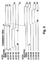
- the CH1 selecting signal 31 turns on (FIG. 3 (a)), and the first terminal 18 of the "channel 1" is connected to the modem section 13 as mentioned earlier.
- the modem section 13 turns on the DR signal and supplies this to the first terminal unit 18 (FIG. 3 (c)).
- the first terminal 18 turns on the RS signal and supplies this to the modem section 13 (FIG. 3 (d)).
- the modem section 13, upon receiving the RS signal 22, turns the CS signal on (FIG.
- the first terminal unit 18 informs the first terminal unit 18 of the data transmission-ready state. Then the first terminal unit 18 supplies the SD signal 23 i.e. transmission data (FIG. 3 (f)). The transmission data undergoes a predetermined modulation in the modem section 13, and is output to the communication line 12.
- the first terminal unit 18 Upon terminating the transmission of the SD signal 23, the first terminal unit 18 turns the RS signal off. As a result, the modem section 13 turns the CS signal off, and further turns the DR signal off. In response to this, the first terminal unit 18 turns the ER signal 21 off at t2.
- the priority controlling circuit 28 detects the off-state of the ER signal 21 and turns the CH1 selecting signal off.
- the CH1 selecting signal 31 When the CH1 selecting signal 31 is in the on-state, if the second terminal unit 19 at the "channel 2" side turns the ER signal 24 on at e.g. t3 (FIG. 3 (h)), the CH2 selecting signal does not immediately turn on since the CH1 selecting signal is already in the on-state, as mentioned earlier. In such a case, there is a wait until the time t2 (FIG. 3 (a)) when the CH1 selecting signal turns off, and then the CH2 se lecting signal 32 turns on.
- the operations after the turning on of the CH2 selecting signal 32 are the same as those of 0aforementioned "channel 1" case, so the communication is car ried out in a sequence as shown in FIG. 3 (g) - (l).
- the priority controlling circuit 28 recognizes this state as a request for setting a priority channel so as to set the CH1 mode setting data 35 supplied from the first terminal unit 18 in the form of the SD signal 23 (FIG. 5 (c)) in the mode register 29 (FIG. 4, Step S103, FIG.5 (g)).
- These data are priority channel data indicating that the "channel 1" will be automatically and preferentially selected hen a call is received.
- the priority controlling circuit 28 will set the CH2 mode setting data 36 supplied from the second terminal unit 19 in the form of the SD signal 26 (FIG. 5 (f)) in the mode register 29 (FIG. 5 (g)).
- the priority controlling circuit 28 reads out the contents of the mode register 29 (Step S104), and discriminates the priority calling channel. If the priority calling channel is "channel 1" (Step S105; Y), the priority controlling circuit 28 turns the CH1 selecting signal 31 on (Step S106), while the CH2 selecting signal 32 is turned on (Step S107) if it is "channel 2" (Step S105; N). Thus, the terminal unit of the channel at the selecting signal on-side is coupled to the modem section 13, and the communication with the opposite station will start in accordance with a predetermined sequence.
- the priority controlling circuit 28 reads out the contents of the mode register 29 (FIG. 6 (f)) and turns the CH1 selecting signal 31 (FIG. 6 (g)) on as mentioned earlier. In consequence, the "channel 1" is selected, and the first terminal unit 18 turns the ER signal 21 (FIG. 6 (b)) on.
- the modem section 13 turns the DR signal (FIG. 6 (c)) on to inform that the communication line 12 is coupled to the modem section 13, and turns the CD signal (FIG. 6 (d)) on.
- the RD signal (FIG. 6 (e)) from the opposite station is received, and thereafter the ER signal 21 as well as the CH1 selecting signal 31 are turned off.
- the earliest call-requested terminal unit among a plurality of terminal units is preferentially selected, while on receiving the call the terminal unit at the side of the priority calling channel previously set in the mode register becomes available.
- the earliest terminal to request the communication-start among a plurality of terminal units coupled to a plurality of input channels is preferentially selected to be the modulator/demodulator, there will be no need for any particular manual operation for starting the communication. Accordingly, the operator can perform the communication without feeling that a single modem device is shared by a plurality of terminal units.
- a single modem device is also advantageously shared in the case of receiving the call by a plurality of terminal units.
Landscapes
- Engineering & Computer Science (AREA)
- Computer Networks & Wireless Communication (AREA)
- Signal Processing (AREA)
- Communication Control (AREA)
Applications Claiming Priority (3)
| Application Number | Priority Date | Filing Date | Title |
|---|---|---|---|
| JP3286541A JPH05130168A (ja) | 1991-10-31 | 1991-10-31 | モデム装置 |
| JP28654191 | 1991-10-31 | ||
| JP286541/91 | 1991-10-31 |
Publications (3)
| Publication Number | Publication Date |
|---|---|
| EP0539964A2 true EP0539964A2 (de) | 1993-05-05 |
| EP0539964A3 EP0539964A3 (en) | 1994-08-10 |
| EP0539964B1 EP0539964B1 (de) | 1999-08-11 |
Family
ID=17705753
Family Applications (1)
| Application Number | Title | Priority Date | Filing Date |
|---|---|---|---|
| EP92118457A Expired - Lifetime EP0539964B1 (de) | 1991-10-31 | 1992-10-28 | Modemvorrichtung |
Country Status (4)
| Country | Link |
|---|---|
| US (1) | US5452329A (de) |
| EP (1) | EP0539964B1 (de) |
| JP (1) | JPH05130168A (de) |
| DE (1) | DE69229769T2 (de) |
Families Citing this family (1)
| Publication number | Priority date | Publication date | Assignee | Title |
|---|---|---|---|---|
| US5628030A (en) * | 1994-03-24 | 1997-05-06 | Multi-Tech Systems, Inc. | Virtual modem driver apparatus and method |
Citations (4)
| Publication number | Priority date | Publication date | Assignee | Title |
|---|---|---|---|---|
| EP0111114A2 (de) * | 1982-11-06 | 1984-06-20 | Telefonbau und Normalzeit GmbH | Schaltungsanordnung für eine Fernsprechvermittlungsanlage, insbesondere Fernsprechnebenstellenanlage mit zusätzlichem Datenverkehr |
| EP0167351A2 (de) * | 1984-06-29 | 1986-01-08 | Northern Telecom Limited | Signalmultiplexschaltung |
| GB2187609A (en) * | 1985-12-16 | 1987-09-09 | British Telecomm | Interfacing data units to a telephone line |
| JPH01149666A (ja) * | 1987-12-07 | 1989-06-12 | Nippon Telegr & Teleph Corp <Ntt> | セレクタブルマルチポートモデム |
Family Cites Families (11)
| Publication number | Priority date | Publication date | Assignee | Title |
|---|---|---|---|---|
| US3633168A (en) * | 1971-03-09 | 1972-01-04 | Ibm | Line control adapter for a synchronous digital-formatted message-communications system |
| JPS5061961A (de) * | 1973-10-01 | 1975-05-27 | ||
| US4040014A (en) * | 1976-09-13 | 1977-08-02 | Sperry Rand Corporation | Modem sharing device |
| US4045774A (en) * | 1976-09-20 | 1977-08-30 | Skei Corporation | Modem sharer |
| US4782498A (en) * | 1986-08-28 | 1988-11-01 | Hayes Microcomputer Products, Inc. | Modem with improved handshaking capability |
| DE3780307T2 (de) * | 1987-04-28 | 1993-02-11 | Ibm | Protokoll und anordnung zur verbindung zwischen einer steuereinheit und mehreren peripheren elementen. |
| US4775983A (en) * | 1987-09-28 | 1988-10-04 | Ncr Corporation | High speed logic analyzer |
| JPH01298854A (ja) * | 1988-05-27 | 1989-12-01 | Oki Electric Ind Co Ltd | データ伝送装置の自動認識方式 |
| JPH02134042A (ja) * | 1988-11-14 | 1990-05-23 | Nec Corp | 回線終端装置 |
| JPH03190340A (ja) * | 1989-12-20 | 1991-08-20 | Nec Corp | 信号分岐装置 |
| JPH0732411B2 (ja) * | 1989-12-27 | 1995-04-10 | 富士通電装株式会社 | 端末切換装置 |
-
1991
- 1991-10-31 JP JP3286541A patent/JPH05130168A/ja active Pending
-
1992
- 1992-10-28 EP EP92118457A patent/EP0539964B1/de not_active Expired - Lifetime
- 1992-10-28 DE DE69229769T patent/DE69229769T2/de not_active Expired - Fee Related
-
1994
- 1994-08-16 US US08/291,140 patent/US5452329A/en not_active Expired - Lifetime
Patent Citations (4)
| Publication number | Priority date | Publication date | Assignee | Title |
|---|---|---|---|---|
| EP0111114A2 (de) * | 1982-11-06 | 1984-06-20 | Telefonbau und Normalzeit GmbH | Schaltungsanordnung für eine Fernsprechvermittlungsanlage, insbesondere Fernsprechnebenstellenanlage mit zusätzlichem Datenverkehr |
| EP0167351A2 (de) * | 1984-06-29 | 1986-01-08 | Northern Telecom Limited | Signalmultiplexschaltung |
| GB2187609A (en) * | 1985-12-16 | 1987-09-09 | British Telecomm | Interfacing data units to a telephone line |
| JPH01149666A (ja) * | 1987-12-07 | 1989-06-12 | Nippon Telegr & Teleph Corp <Ntt> | セレクタブルマルチポートモデム |
Non-Patent Citations (2)
| Title |
|---|
| IBM TECHNICAL DISCLOSURE BULLETIN, vol.27, no.9, February 1985, NEW YORK US pages 5270 - 5271 M.CUKIER ET AL. 'Serial interface between a modem and a data multiplexing box.' * |
| PATENT ABSTRACTS OF JAPAN vol. 13, no. 410 (E-819) (3758) 11 September 1989 & JP-A-01 149 666 (NTT) 12 June 1989 * |
Also Published As
| Publication number | Publication date |
|---|---|
| EP0539964B1 (de) | 1999-08-11 |
| JPH05130168A (ja) | 1993-05-25 |
| EP0539964A3 (en) | 1994-08-10 |
| DE69229769D1 (de) | 1999-09-16 |
| DE69229769T2 (de) | 2000-03-02 |
| US5452329A (en) | 1995-09-19 |
Similar Documents
| Publication | Publication Date | Title |
|---|---|---|
| US5519763A (en) | Communication apparatus with wireless intercommunication | |
| US4746986A (en) | Manifold analog/digital facsimile apparatus | |
| EP0390931A1 (de) | Verfahren zur betriebsartanpassung eines modems | |
| JPS5946143B2 (ja) | 双方向catvシステムにおける伝送確認方法および装置 | |
| CA1286410C (en) | Remote monitoring system receiver with dual baud rate selector | |
| US4405951A (en) | Facsimile control system | |
| US5452329A (en) | Modem device | |
| EP0683588A2 (de) | Schnurlose Reihenanlage | |
| EP0033821A2 (de) | Intelligente Schnittstelle zur automatischen Steuerung einer geschalteten oder Standübertragungsleitung | |
| KR960002844B1 (ko) | 전력선 통신용 신호 변환장치 | |
| JPS5999846A (ja) | フアクシミリ通信装置 | |
| JP2619652B2 (ja) | データ伝送装置 | |
| JPS62178066A (ja) | フアクシミリシステム | |
| JP2545618Y2 (ja) | モデム装置 | |
| JPS588184B2 (ja) | 切分試験方法 | |
| JP3452376B2 (ja) | 2線/4線変換用アダプタ装置 | |
| JPH054368Y2 (de) | ||
| JPS6117428B2 (de) | ||
| JP2911714B2 (ja) | 着信機能切替装置 | |
| KR920011066B1 (ko) | 데이타 변복조기와 다이얼-업 모뎀의 다이얼 신호 인터페이스회로 | |
| JPH02270444A (ja) | 2線全二重/半二重切替装置 | |
| CS259790B1 (cs) | Zapojení pro přenos dat po duplexním datovém spoji | |
| JPH06177874A (ja) | Isdnデータ伝送装置 | |
| JP2575514B2 (ja) | データ通信装置 | |
| JPH04360350A (ja) | 変復調器接続方式 |
Legal Events
| Date | Code | Title | Description |
|---|---|---|---|
| PUAI | Public reference made under article 153(3) epc to a published international application that has entered the european phase |
Free format text: ORIGINAL CODE: 0009012 |
|
| AK | Designated contracting states |
Kind code of ref document: A2 Designated state(s): DE FR GB |
|
| PUAL | Search report despatched |
Free format text: ORIGINAL CODE: 0009013 |
|
| AK | Designated contracting states |
Kind code of ref document: A3 Designated state(s): DE FR GB |
|
| 17P | Request for examination filed |
Effective date: 19941025 |
|
| 17Q | First examination report despatched |
Effective date: 19971006 |
|
| GRAG | Despatch of communication of intention to grant |
Free format text: ORIGINAL CODE: EPIDOS AGRA |
|
| RAP1 | Party data changed (applicant data changed or rights of an application transferred) |
Owner name: SANYO ELECTRIC CO., LTD. |
|
| GRAG | Despatch of communication of intention to grant |
Free format text: ORIGINAL CODE: EPIDOS AGRA |
|
| GRAH | Despatch of communication of intention to grant a patent |
Free format text: ORIGINAL CODE: EPIDOS IGRA |
|
| GRAH | Despatch of communication of intention to grant a patent |
Free format text: ORIGINAL CODE: EPIDOS IGRA |
|
| GRAA | (expected) grant |
Free format text: ORIGINAL CODE: 0009210 |
|
| AK | Designated contracting states |
Kind code of ref document: B1 Designated state(s): DE FR GB |
|
| REF | Corresponds to: |
Ref document number: 69229769 Country of ref document: DE Date of ref document: 19990916 |
|
| ET | Fr: translation filed | ||
| PLBE | No opposition filed within time limit |
Free format text: ORIGINAL CODE: 0009261 |
|
| STAA | Information on the status of an ep patent application or granted ep patent |
Free format text: STATUS: NO OPPOSITION FILED WITHIN TIME LIMIT |
|
| 26N | No opposition filed | ||
| REG | Reference to a national code |
Ref country code: GB Ref legal event code: IF02 |
|
| PGFP | Annual fee paid to national office [announced via postgrant information from national office to epo] |
Ref country code: FR Payment date: 20031003 Year of fee payment: 12 |
|
| PGFP | Annual fee paid to national office [announced via postgrant information from national office to epo] |
Ref country code: GB Payment date: 20031022 Year of fee payment: 12 |
|
| PGFP | Annual fee paid to national office [announced via postgrant information from national office to epo] |
Ref country code: DE Payment date: 20031103 Year of fee payment: 12 |
|
| PG25 | Lapsed in a contracting state [announced via postgrant information from national office to epo] |
Ref country code: GB Free format text: LAPSE BECAUSE OF NON-PAYMENT OF DUE FEES Effective date: 20041028 |
|
| PG25 | Lapsed in a contracting state [announced via postgrant information from national office to epo] |
Ref country code: DE Free format text: LAPSE BECAUSE OF NON-PAYMENT OF DUE FEES Effective date: 20050503 |
|
| GBPC | Gb: european patent ceased through non-payment of renewal fee |
Effective date: 20041028 |
|
| PG25 | Lapsed in a contracting state [announced via postgrant information from national office to epo] |
Ref country code: FR Free format text: LAPSE BECAUSE OF NON-PAYMENT OF DUE FEES Effective date: 20050630 |
|
| REG | Reference to a national code |
Ref country code: FR Ref legal event code: ST |