EP0510349B1 - Verfahren zur Herstellung eines MOS-Transistors - Google Patents
Verfahren zur Herstellung eines MOS-Transistors Download PDFInfo
- Publication number
- EP0510349B1 EP0510349B1 EP92104520A EP92104520A EP0510349B1 EP 0510349 B1 EP0510349 B1 EP 0510349B1 EP 92104520 A EP92104520 A EP 92104520A EP 92104520 A EP92104520 A EP 92104520A EP 0510349 B1 EP0510349 B1 EP 0510349B1
- Authority
- EP
- European Patent Office
- Prior art keywords
- layer
- insulation
- substrate
- gate electrode
- doped
- Prior art date
- Legal status (The legal status is an assumption and is not a legal conclusion. Google has not performed a legal analysis and makes no representation as to the accuracy of the status listed.)
- Expired - Lifetime
Links
Images

Classifications
-
- H—ELECTRICITY
- H10—SEMICONDUCTOR DEVICES; ELECTRIC SOLID-STATE DEVICES NOT OTHERWISE PROVIDED FOR
- H10D—INORGANIC ELECTRIC SEMICONDUCTOR DEVICES
- H10D62/00—Semiconductor bodies, or regions thereof, of devices having potential barriers
- H10D62/10—Shapes, relative sizes or dispositions of the regions of the semiconductor bodies; Shapes of the semiconductor bodies
- H10D62/17—Semiconductor regions connected to electrodes not carrying current to be rectified, amplified or switched, e.g. channel regions
- H10D62/213—Channel regions of field-effect devices
- H10D62/221—Channel regions of field-effect devices of FETs
- H10D62/228—Channel regions of field-effect devices of FETs having delta-doped channels
-
- H—ELECTRICITY
- H10—SEMICONDUCTOR DEVICES; ELECTRIC SOLID-STATE DEVICES NOT OTHERWISE PROVIDED FOR
- H10D—INORGANIC ELECTRIC SEMICONDUCTOR DEVICES
- H10D30/00—Field-effect transistors [FET]
- H10D30/60—Insulated-gate field-effect transistors [IGFET]
-
- H—ELECTRICITY
- H10—SEMICONDUCTOR DEVICES; ELECTRIC SOLID-STATE DEVICES NOT OTHERWISE PROVIDED FOR
- H10D—INORGANIC ELECTRIC SEMICONDUCTOR DEVICES
- H10D62/00—Semiconductor bodies, or regions thereof, of devices having potential barriers
- H10D62/01—Manufacture or treatment
- H10D62/021—Forming source or drain recesses by etching e.g. recessing by etching and then refilling
-
- H—ELECTRICITY
- H10—SEMICONDUCTOR DEVICES; ELECTRIC SOLID-STATE DEVICES NOT OTHERWISE PROVIDED FOR
- H10D—INORGANIC ELECTRIC SEMICONDUCTOR DEVICES
- H10D62/00—Semiconductor bodies, or regions thereof, of devices having potential barriers
- H10D62/10—Shapes, relative sizes or dispositions of the regions of the semiconductor bodies; Shapes of the semiconductor bodies
- H10D62/17—Semiconductor regions connected to electrodes not carrying current to be rectified, amplified or switched, e.g. channel regions
- H10D62/213—Channel regions of field-effect devices
- H10D62/221—Channel regions of field-effect devices of FETs
- H10D62/235—Channel regions of field-effect devices of FETs of IGFETs
- H10D62/314—Channel regions of field-effect devices of FETs of IGFETs having vertical doping variations
Definitions
- MOS transistors With the general development towards larger packing densities in integrated circuits, MOS transistors with reduced space requirements are also required. When the structure of a MOS transistor is reduced, the gate length is also shortened.
- a delta-doped layer has a thickness of approximately 20 nm. It is doped with the opposite conductivity type as the source and drain region. It has a dopant concentration of more than 10 19 cm -3 . In comparison to the conventional anti-punch implantation, which forms a smeared distribution in the substrate, the dopant concentration in delta-doped layers is localized sharply.
- the invention is therefore based on the problem of specifying a method for producing a MOS transistor with a delta-shaped doped layer which is suitable for integration into the manufacturing process of a ULSI integrated circuit.
- the layer growth during epitaxial growth can be controlled very precisely. Furthermore, use is made of the fact that in epitaxial growth from the gas phase by adding dopant-containing gases, doped layers can be produced. The doping of these can be adjusted very precisely via the gas concentration and the thickness via the layer growth.
- the process according to the invention therefore has the advantage that the second layer, which acts as a delta-shaped layer, can be easily controlled in a thickness of, for. B. 20 nm can be produced.
- the thickness of the third layer arranged above it, in which the channel forms in the finished transistor, can also be adjusted in a controllable manner via the layer growth.
- the MOS transistor is self-aligned surrounded by an isolation structure.
- the insulation layer and the insulation structure are made of one material to which the first layer, the second layer and the third layer can be selectively etched.
- recesses reaching into the first layer are produced selectively with respect to the insulation layer and the insulation structure on both sides of the gate electrode.
- a glass layer is then applied over the entire surface, which is provided with dopant of the second conductivity type.
- the source and drain regions are formed by driving the dopant into the exposed surfaces of the first layer, the second layer and the third layer.
- the tempering step must be carried out in such a way that the dopant distribution in the second layer, which acts as a delta-shaped layer, and in the third layer remains essentially unchanged. It is within the scope of the invention to carry out the tempering step in a short-term healing process.
- the insulation structure is particularly advantageous to produce the insulation structure by forming a first insulation layer on the gate electrode.
- the first insulation layer has flanks that are common to the gate electrode and perpendicular to the surface of the substrate.
- Flank insulation also called spacer, is generated on the flanks by conformal deposition over the entire surface and subsequent anisotropic etching back of a second insulation layer.
- the arrangement of the source and drain regions to the gate electrode and to the insulation layer is self-aligned.
- the distance between the gate electrode and the source or drain region is determined by the width of the edge insulation. This width of the edge insulation is only dependent on the thickness in which the second insulation layer is deposited. This eliminates the need for a mask step to define the source and drain regions.
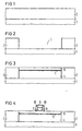
- An insulation layer 2 is applied to a substrate 1 (see FIG. 1).
- a substrate 1 z. B. uses a p-doped substrate made of monocrystalline silicon with 100 surface orientation.
- the insulation layer 2 is after known input cleaning steps in a thickness of z. B. 400 nm grown from SiO 2 . This is done e.g. B. thermally or via a separator.
- the insulation layer 2 is structured so that it has an opening 3.
- the surface of the substrate 1 is exposed within the opening 3 (see FIG. 2).
- the opening 3 defines an area for a MOS transistor.
- a first layer 4, a second layer 5 and a third layer 6 are then produced in the opening 3 in such a way that the opening 3 is essentially filled (see FIG. 3).
- the first layer 4 is deposited undoped in a thickness of e.g. B. 300 nm.
- the second layer 5 is z. B. p-doped deposited in a thickness of z. B. 20 nm. The doping takes place z. B. by adding boron in a concentration of at least 10 19 cm -3 .
- the third layer 6 is deposited n-doped. It has a thickness of approximately 100 nm.
- the gate dielectric 7 consists, for. B. from SiO 2 or from a nitride / SiO 2 compound.
- a gate electrode 8 is generated above the gate dielectric 7. This is done e.g. B. by full-surface deposition of a polysilicon layer that is doped via ion implantation or occupancy.
- An oxide layer is deposited on the polysilicon layer using a CVD process. This double layer consisting of the polysilicon layer and the oxide layer is structured phototechnically. This results in the gate electrode 8 and a first oxide layer 9.
- first oxide layer 9 and the gate electrode 8 have common flanks that are perpendicular to the surface of the substrate 1.
- a second oxide layer is then deposited conformally.
- the second oxide layer is anisotropically etched back with the aid of dry etching, so that flank insulation 10 made of SiO 2 is formed on both sides of the gate electrode 9 and the first oxide layer 9.
- the term spacer is also used for the edge insulation 10.
- the width of the edge insulation 10 on the surface of the third layer 6 is given by the thickness of the second oxide layer.
- edge insulation 10 care must be taken that the SiO 2 etching is coated to such an extent that the surface of the third layer 6 outside the gate electrode 9 and the edge insulation 10 is completely exposed, so that the bare silicon crystal is revealed.
- depressions 11 are produced on the side of the gate electrode 8 within the insulation layer 2 (see FIG. 5).
- the depressions 11 extend into the first layer 4, so that the second layer 5 and the third layer 6 are completely removed to the side of the flank insulation 10.
- a z. B. arsenic-doped glass layer 12 conformally deposited. Through easy Expulsion of the dopant at z. B. 1000 - 1050 ° C during z. B. 10 seconds.
- a source region 13 and a drain region 14 are formed on the surfaces of the first layer 4, the second layer 5 and the third layer 6, which are in contact with the glass layer 12.
- the temperature step must be carried out in such a way that the second layer 5, which acts as a delta-doped layer, diverges only insignificantly (see FIG. 6).
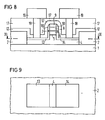
- the MOS transistor is then completed by planarization, contact hole etching and metallization. This is done e.g. B. (see FIG. 7) by full-surface deposition of a dielectric 15. In the dielectric 15 and the glass layer 12, contact holes are opened above the source region 13 and drain region 14, which are filled with metallizations 16.
- the MOS transistor is completed in that a planarizing layer 17 of z. B. BPSG is deposited.
- a planarizing layer 17 of z. B. BPSG is deposited.
- contact holes are opened onto the source region 13 and the drain region 14.
- the contact holes are filled with tungsten 18.
- Tungsten fillings 18 covering aluminum contacts 19 are applied to the surface of planarizing layer 17 (see FIG. 8).
- the section indicated by IX-IX in FIGS. 7 and 8 can be seen in FIG. 9.
- the MOS transistor is completely surrounded by the insulation layer 2.
- the method was described using the example of an NMOS transistor. It can be transferred completely analog to a PMOS transistor.
Landscapes
- Insulated Gate Type Field-Effect Transistor (AREA)
- Metal-Oxide And Bipolar Metal-Oxide Semiconductor Integrated Circuits (AREA)
- Thin Film Transistor (AREA)
Applications Claiming Priority (2)
| Application Number | Priority Date | Filing Date | Title |
|---|---|---|---|
| DE4113755 | 1991-04-26 | ||
| DE4113755 | 1991-04-26 |
Publications (2)
| Publication Number | Publication Date |
|---|---|
| EP0510349A1 EP0510349A1 (de) | 1992-10-28 |
| EP0510349B1 true EP0510349B1 (de) | 1996-06-05 |
Family
ID=6430471
Family Applications (1)
| Application Number | Title | Priority Date | Filing Date |
|---|---|---|---|
| EP92104520A Expired - Lifetime EP0510349B1 (de) | 1991-04-26 | 1992-03-16 | Verfahren zur Herstellung eines MOS-Transistors |
Country Status (7)
| Country | Link |
|---|---|
| US (1) | US5212104A (enExample) |
| EP (1) | EP0510349B1 (enExample) |
| JP (1) | JPH05145070A (enExample) |
| KR (1) | KR100313469B1 (enExample) |
| AT (1) | ATE139060T1 (enExample) |
| DE (1) | DE59206456D1 (enExample) |
| TW (1) | TW211081B (enExample) |
Families Citing this family (6)
| Publication number | Priority date | Publication date | Assignee | Title |
|---|---|---|---|---|
| JPH04299569A (ja) * | 1991-03-27 | 1992-10-22 | Nec Corp | Soisの製造方法及びトランジスタとその製造方法 |
| US5559368A (en) * | 1994-08-30 | 1996-09-24 | The Regents Of The University Of California | Dynamic threshold voltage mosfet having gate to body connection for ultra-low voltage operation |
| WO2001093339A1 (en) * | 2000-05-31 | 2001-12-06 | Matsushita Electric Industrial Co. Ltd. | Misfet |
| US6580137B2 (en) | 2000-08-29 | 2003-06-17 | Boise State University | Damascene double gated transistors and related manufacturing methods |
| DE102006009226B9 (de) * | 2006-02-28 | 2011-03-10 | Advanced Micro Devices, Inc., Sunnyvale | Verfahren zum Herstellen eines Transistors mit einer erhöhten Schwellwertstabilität ohne Durchlass-Strombeeinträchtigung und Transistor |
| KR20230032984A (ko) * | 2021-08-31 | 2023-03-07 | 인벤션 앤드 콜라보레이션 라보라토리 피티이. 엘티디. | 표준 셀 구조 |
Family Cites Families (8)
| Publication number | Priority date | Publication date | Assignee | Title |
|---|---|---|---|---|
| DE2911726C2 (de) * | 1978-03-27 | 1985-08-01 | Ncr Corp., Dayton, Ohio | Verfahren zur Herstellung eines Feldeffekttransistors |
| JPS5750452A (en) * | 1980-09-12 | 1982-03-24 | Fujitsu Ltd | Semiconductor device |
| JPS58157169A (ja) * | 1982-03-15 | 1983-09-19 | Sharp Corp | 半導体装置 |
| JPS5910278A (ja) * | 1983-06-24 | 1984-01-19 | Hitachi Ltd | 半導体装置 |
| JPS59188175A (ja) * | 1984-02-01 | 1984-10-25 | Hitachi Ltd | 半導体装置 |
| JPS61116875A (ja) * | 1985-11-13 | 1986-06-04 | Hitachi Ltd | 半導体装置 |
| US4908678A (en) * | 1986-10-08 | 1990-03-13 | Semiconductor Energy Laboratory Co., Ltd. | FET with a super lattice channel |
| JPH01204411A (ja) * | 1988-02-09 | 1989-08-17 | Nec Corp | 半導体装置の製造方法 |
-
1992
- 1992-03-09 US US07/848,238 patent/US5212104A/en not_active Expired - Fee Related
- 1992-03-16 EP EP92104520A patent/EP0510349B1/de not_active Expired - Lifetime
- 1992-03-16 AT AT92104520T patent/ATE139060T1/de not_active IP Right Cessation
- 1992-03-16 DE DE59206456T patent/DE59206456D1/de not_active Expired - Fee Related
- 1992-04-21 TW TW081103106A patent/TW211081B/zh active
- 1992-04-22 JP JP4130120A patent/JPH05145070A/ja not_active Withdrawn
- 1992-04-27 KR KR1019920007106A patent/KR100313469B1/ko not_active Expired - Fee Related
Also Published As
| Publication number | Publication date |
|---|---|
| DE59206456D1 (de) | 1996-07-11 |
| KR100313469B1 (ko) | 2001-12-28 |
| KR920020758A (ko) | 1992-11-21 |
| JPH05145070A (ja) | 1993-06-11 |
| ATE139060T1 (de) | 1996-06-15 |
| TW211081B (enExample) | 1993-08-11 |
| EP0510349A1 (de) | 1992-10-28 |
| US5212104A (en) | 1993-05-18 |
Similar Documents
| Publication | Publication Date | Title |
|---|---|---|
| DE69217682T2 (de) | Verfahren zur Herstellung von Halbleiteranordnungen und integrierten Schaltkreisen mit Verwendung von Seitenwand-Abstandsstücken | |
| DE69521579T2 (de) | Herstellungsverfahren für MOS-Halbleiterbauelement | |
| DE69901657T2 (de) | Herstellungsverfahren für selbstjustierende lokale Zwischenverbindung | |
| DE69209678T2 (de) | Halbleiteranordnung für Hochspannungsverwendung und Verfahren zur Herstellung | |
| DE112005002302B4 (de) | Verfahren zur Herstellung von Metallgate-Transistoren mit epitaktischen Source- und Drainregionen und MOS-Transistor | |
| DE3587231T2 (de) | Verfahren zum herstellen einer dmos-halbleiteranordnung. | |
| DE112005000704B4 (de) | Nicht-planarer Bulk-Transistor mit verspanntem Kanal mit erhöhter Mobilität und Verfahren zur Herstellung | |
| DE3886074T2 (de) | Herstellung einer Halbleiterstruktur. | |
| EP0809860B1 (de) | Verfahren zur Herstellung einer SCHICHTSTRUKTUR MIT EINER SILICID-SCHICHT | |
| EP0118709A2 (de) | Verfahren zum Herstellen von MOS-Transistoren mit flachen Source/Drain-Gebieten, kurzen Kanallängen und einer selbstjustierten, aus einem Metallsilizid bestehenden Kontaktierungsebene | |
| DE4332074A1 (de) | Halbleiterspeichereinrichtung und Verfahren zu ihrer Herstellung | |
| DE19525069C1 (de) | Verfahren zur Herstellung einer integrierten CMOS-Schaltung | |
| EP0482232A1 (de) | Verfahren zur Herstellung einer dotierten Polyzidschicht auf einem Halbleitersubstrat | |
| DE4101130C2 (de) | MOS-Feldeffekttransistor und Verfahren zu dessen Herstellung | |
| DE102012223653A1 (de) | Mosfet mit V-Nut-Source/Drain-Zone und Verfahren zur Herstellung desselben | |
| DE19535629C1 (de) | Verfahren zur Herstellung einer integrierten CMOS-Schaltung | |
| DE19720193C2 (de) | Integrierte Schaltungsanordnung mit mindestens zwei vertikalen MOS-Transistoren und Verfahren zu deren Herstellung | |
| EP0159617B1 (de) | Verfahren zum Herstellen von hochintegrierten MOS-Feldeffekttransistoren | |
| DE19933564C1 (de) | Verfahren zur Herstellung eines Vertikal-Halbleitertransistorbauelements und Vertikal-Halbleitertransistorbauelement | |
| EP0510349B1 (de) | Verfahren zur Herstellung eines MOS-Transistors | |
| EP1181723B1 (de) | Doppel-gate-mosfet-transistor und verfahren zu seiner herstellung | |
| DE102006029701B4 (de) | Halbleiterbauteil sowie Verfahren zur Herstellung eines Halbleiterbauteils | |
| DE102006029229A1 (de) | Herstellungsverfahren für eine integrierte Halbleiterstruktur und entsprechende integrierte Halbleiterstruktur | |
| EP0864172B1 (de) | Verfahren zur herstellung einer integrierten schaltungsanordnung mit mindestens einem mos-transistor | |
| DE69322024T2 (de) | Verfahren zur Herstellung eines leitenden Kontakts auf einem Halbleiterkörper |
Legal Events
| Date | Code | Title | Description |
|---|---|---|---|
| PUAI | Public reference made under article 153(3) epc to a published international application that has entered the european phase |
Free format text: ORIGINAL CODE: 0009012 |
|
| AK | Designated contracting states |
Kind code of ref document: A1 Designated state(s): AT DE FR GB IT NL |
|
| 17P | Request for examination filed |
Effective date: 19921124 |
|
| 17Q | First examination report despatched |
Effective date: 19950111 |
|
| GRAA | (expected) grant |
Free format text: ORIGINAL CODE: 0009210 |
|
| AK | Designated contracting states |
Kind code of ref document: B1 Designated state(s): AT DE FR GB IT NL |
|
| REF | Corresponds to: |
Ref document number: 139060 Country of ref document: AT Date of ref document: 19960615 Kind code of ref document: T |
|
| REF | Corresponds to: |
Ref document number: 59206456 Country of ref document: DE Date of ref document: 19960711 |
|
| ET | Fr: translation filed | ||
| ITF | It: translation for a ep patent filed | ||
| GBT | Gb: translation of ep patent filed (gb section 77(6)(a)/1977) |
Effective date: 19960813 |
|
| PLBE | No opposition filed within time limit |
Free format text: ORIGINAL CODE: 0009261 |
|
| STAA | Information on the status of an ep patent application or granted ep patent |
Free format text: STATUS: NO OPPOSITION FILED WITHIN TIME LIMIT |
|
| 26N | No opposition filed | ||
| PGFP | Annual fee paid to national office [announced via postgrant information from national office to epo] |
Ref country code: NL Payment date: 19980320 Year of fee payment: 7 |
|
| PGFP | Annual fee paid to national office [announced via postgrant information from national office to epo] |
Ref country code: AT Payment date: 19990303 Year of fee payment: 8 |
|
| PG25 | Lapsed in a contracting state [announced via postgrant information from national office to epo] |
Ref country code: NL Free format text: LAPSE BECAUSE OF NON-PAYMENT OF DUE FEES Effective date: 19991001 |
|
| NLV4 | Nl: lapsed or anulled due to non-payment of the annual fee |
Effective date: 19991001 |
|
| PG25 | Lapsed in a contracting state [announced via postgrant information from national office to epo] |
Ref country code: AT Free format text: LAPSE BECAUSE OF NON-PAYMENT OF DUE FEES Effective date: 20000316 |
|
| PGFP | Annual fee paid to national office [announced via postgrant information from national office to epo] |
Ref country code: DE Payment date: 20010530 Year of fee payment: 10 |
|
| REG | Reference to a national code |
Ref country code: GB Ref legal event code: IF02 |
|
| PGFP | Annual fee paid to national office [announced via postgrant information from national office to epo] |
Ref country code: GB Payment date: 20020305 Year of fee payment: 11 |
|
| PGFP | Annual fee paid to national office [announced via postgrant information from national office to epo] |
Ref country code: FR Payment date: 20020326 Year of fee payment: 11 |
|
| PG25 | Lapsed in a contracting state [announced via postgrant information from national office to epo] |
Ref country code: DE Free format text: LAPSE BECAUSE OF NON-PAYMENT OF DUE FEES Effective date: 20021001 |
|
| PG25 | Lapsed in a contracting state [announced via postgrant information from national office to epo] |
Ref country code: GB Free format text: LAPSE BECAUSE OF NON-PAYMENT OF DUE FEES Effective date: 20030316 |
|
| GBPC | Gb: european patent ceased through non-payment of renewal fee |
Effective date: 20030316 |
|
| PG25 | Lapsed in a contracting state [announced via postgrant information from national office to epo] |
Ref country code: FR Free format text: LAPSE BECAUSE OF NON-PAYMENT OF DUE FEES Effective date: 20031127 |
|
| REG | Reference to a national code |
Ref country code: FR Ref legal event code: ST |
|
| PG25 | Lapsed in a contracting state [announced via postgrant information from national office to epo] |
Ref country code: IT Free format text: LAPSE BECAUSE OF NON-PAYMENT OF DUE FEES;WARNING: LAPSES OF ITALIAN PATENTS WITH EFFECTIVE DATE BEFORE 2007 MAY HAVE OCCURRED AT ANY TIME BEFORE 2007. THE CORRECT EFFECTIVE DATE MAY BE DIFFERENT FROM THE ONE RECORDED. Effective date: 20050316 |