EP0509490A2 - Flüssigkristallgerät - Google Patents
Flüssigkristallgerät Download PDFInfo
- Publication number
- EP0509490A2 EP0509490A2 EP92106552A EP92106552A EP0509490A2 EP 0509490 A2 EP0509490 A2 EP 0509490A2 EP 92106552 A EP92106552 A EP 92106552A EP 92106552 A EP92106552 A EP 92106552A EP 0509490 A2 EP0509490 A2 EP 0509490A2
- Authority
- EP
- European Patent Office
- Prior art keywords
- liquid crystal
- substrates
- crystal apparatus
- stripe
- pair
- Prior art date
- Legal status (The legal status is an assumption and is not a legal conclusion. Google has not performed a legal analysis and makes no representation as to the accuracy of the status listed.)
- Ceased
Links
Images


Classifications
-
- G—PHYSICS
- G02—OPTICS
- G02F—OPTICAL DEVICES OR ARRANGEMENTS FOR THE CONTROL OF LIGHT BY MODIFICATION OF THE OPTICAL PROPERTIES OF THE MEDIA OF THE ELEMENTS INVOLVED THEREIN; NON-LINEAR OPTICS; FREQUENCY-CHANGING OF LIGHT; OPTICAL LOGIC ELEMENTS; OPTICAL ANALOGUE/DIGITAL CONVERTERS
- G02F1/00—Devices or arrangements for the control of the intensity, colour, phase, polarisation or direction of light arriving from an independent light source, e.g. switching, gating or modulating; Non-linear optics
- G02F1/01—Devices or arrangements for the control of the intensity, colour, phase, polarisation or direction of light arriving from an independent light source, e.g. switching, gating or modulating; Non-linear optics for the control of the intensity, phase, polarisation or colour
- G02F1/13—Devices or arrangements for the control of the intensity, colour, phase, polarisation or direction of light arriving from an independent light source, e.g. switching, gating or modulating; Non-linear optics for the control of the intensity, phase, polarisation or colour based on liquid crystals, e.g. single liquid crystal display cells
- G02F1/133—Constructional arrangements; Operation of liquid crystal cells; Circuit arrangements
- G02F1/1333—Constructional arrangements; Manufacturing methods
- G02F1/133371—Cells with varying thickness of the liquid crystal layer
-
- G—PHYSICS
- G02—OPTICS
- G02F—OPTICAL DEVICES OR ARRANGEMENTS FOR THE CONTROL OF LIGHT BY MODIFICATION OF THE OPTICAL PROPERTIES OF THE MEDIA OF THE ELEMENTS INVOLVED THEREIN; NON-LINEAR OPTICS; FREQUENCY-CHANGING OF LIGHT; OPTICAL LOGIC ELEMENTS; OPTICAL ANALOGUE/DIGITAL CONVERTERS
- G02F1/00—Devices or arrangements for the control of the intensity, colour, phase, polarisation or direction of light arriving from an independent light source, e.g. switching, gating or modulating; Non-linear optics
- G02F1/01—Devices or arrangements for the control of the intensity, colour, phase, polarisation or direction of light arriving from an independent light source, e.g. switching, gating or modulating; Non-linear optics for the control of the intensity, phase, polarisation or colour
- G02F1/13—Devices or arrangements for the control of the intensity, colour, phase, polarisation or direction of light arriving from an independent light source, e.g. switching, gating or modulating; Non-linear optics for the control of the intensity, phase, polarisation or colour based on liquid crystals, e.g. single liquid crystal display cells
- G02F1/137—Devices or arrangements for the control of the intensity, colour, phase, polarisation or direction of light arriving from an independent light source, e.g. switching, gating or modulating; Non-linear optics for the control of the intensity, phase, polarisation or colour based on liquid crystals, e.g. single liquid crystal display cells characterised by the electro-optical or magneto-optical effect, e.g. field-induced phase transition, orientation effect, guest-host interaction or dynamic scattering
- G02F1/139—Devices or arrangements for the control of the intensity, colour, phase, polarisation or direction of light arriving from an independent light source, e.g. switching, gating or modulating; Non-linear optics for the control of the intensity, phase, polarisation or colour based on liquid crystals, e.g. single liquid crystal display cells characterised by the electro-optical or magneto-optical effect, e.g. field-induced phase transition, orientation effect, guest-host interaction or dynamic scattering based on orientation effects in which the liquid crystal remains transparent
- G02F1/141—Devices or arrangements for the control of the intensity, colour, phase, polarisation or direction of light arriving from an independent light source, e.g. switching, gating or modulating; Non-linear optics for the control of the intensity, phase, polarisation or colour based on liquid crystals, e.g. single liquid crystal display cells characterised by the electro-optical or magneto-optical effect, e.g. field-induced phase transition, orientation effect, guest-host interaction or dynamic scattering based on orientation effects in which the liquid crystal remains transparent using ferroelectric liquid crystals
Definitions
- the present invention relates to a liquid crystal apparatus such as a display apparatus using a chiral smectic liquid crystal which shows ferroelectricity.
- Display apparatus using a ferroelectric chiral smectic liquid crystal have been known as disclosed in, e.g., U.S. Patents Nos. 4,639,089, 4,681,404, 4,682,858, 4,712,873, 4,712,874, 4,712,875, 4,712,877, 4,714,323, 4,718,276, 4,738,515, 4,740,060, 4,765,720, 4,778,259, 4,796,979, 4,796,980, 4,859,036, 4,932,757, 4,932,758, 5,000,545 and 5,007,716.
- Such a display apparatus includes a liquid crystal device comprising a cell structure formed by disposing a pair of glass plates each provided with transparent electrodes and an aligning treatment on their inner sides opposite to each other with a cell gap on the order of 1 to 3 ⁇ m and a ferroelectric chiral smectic liquid crystal (hereinafter sometimes abbreviated as "FLC”) filling the cell gap.
- a liquid crystal device comprising a cell structure formed by disposing a pair of glass plates each provided with transparent electrodes and an aligning treatment on their inner sides opposite to each other with a cell gap on the order of 1 to 3 ⁇ m and a ferroelectric chiral smectic liquid crystal (hereinafter sometimes abbreviated as "FLC”) filling the cell gap.
- FLC ferroelectric chiral smectic liquid crystal
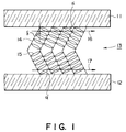
- Figure 1 is a sectional view showing an alignment state of FLC 13 disposed between substrates 11 and 12.
- the FLC 13 forms a plurality of layers 14 each comprising plural liquid crystal molecules 15.
- the layers 14 are aligned substantially in a direction and each layer 15 is bent between the substrates.
- the long axis of each liquid crystal molecule 15 may preferably be inclined to form a pretilt angle ⁇ of at least 5 degrees with respect to the substrates 11 and 12.
- the above-mentioned alignment state may preferably be formed by providing unidirectional alignment axes 16 and 17, which are parallel and in the same direction, to the substrates 11 and 12, e.g., by rubbing.
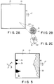
- Figure 2 (including Figures 2A - 2C) is a plan view of a device in which FLC 13 assumes a chevron structure as described with reference to Figure 1.
- the device in Figure 2 is constituted by fixing the substrates 11 and 12 having unidirectional rubbing axes 16 and 17, respectively, to each other by means of a sealant 21 to leave a space which is filled with FLC 13.
- the substrate 11 is provided with a first group of plural stripe electrodes for voltage application (not shown), and the substrate 12 is provided with a second group of plural stripe electrodes (not shown) intersecting the first group of stripe electrodes, thus forming an electrode matrix.
- the normal 22 with a vector n s to the layers 14 of FLC 13 is substantially parallel to the rubbing directions 16 and 17 as shown in Figure 2B.
- the liquid crystal molecules 15 in the device shown in Figure 2 are uniformly oriented leftwards at a tilt angle + ⁇ with their spontaneous polarization directing from the front face to the back face of the drawing.
- liquid crystal molecules 15 in Figure 2B were uniformly oriented rightwards at a tilt angle - ⁇ with their spontaneous polarization directing from the back face to the front face of the drawing, the liquid crystal molecules 15 were found to move leftwards in contrast to the above.
- An object of the present invention is to provide a liquid crystal apparatus having solved the above-mentioned problem.
- a liquid crystal apparatus comprising:
- a liquid crystal apparatus comprising:
- Figure 1 is a sectional view showing an alignment state of liquid crystal used in the present invention.
- Figure 2A shows a plan view corresponding to Figure 1
- Figure 2B is a partially enlarged view of Figure 2A
- Figure 2C is a partially enlarged view of Figure 2B.
- Figure 3 is a plan view showing an alignment state in a conventional device.
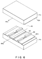
- Figure 4 is a perspective view showing a structure of a liquid crystal panel according to the present invention.
- Figure 5 is a sectional view of such a liquid crystal panel according to the present invention.
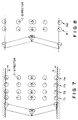
- Figure 6 is a perspective view showing a structure of another liquid crystal panel according to the present invention.
- Figures 7 and 8 are explanatory views for illustrating changes in director orientation according to various positions between substrates in C1 alignment and C2 alignment, respectively.
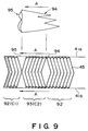
- Figure 9 is an explanatory view for illustrating an alignment state occurring in a chiral smectic liquid crystal used in the present invention.
- Figures 10 and 11 are respectively a sectional view of stripe transparent electrodes provided with stripe conductor films.
- Figure 12 is a graph showing a relationship between the velocity of liquid crystal molecular movement and the thickness and pitch of stripe conductor films on the stripe transparent electrodes.
- Figure 13 is a block diagram of a liquid crystal apparatus of the present invention.
- Figures 14 and 15 are waveform diagrams showing drive voltage waveforms supplied from a drive apparatus used in the present invention.
- Figure 4 is a perspective view schematically illustrating a liquid crystal cell for constituting an embodiment of the present invention
- Figure 5 is a sectional view taken along a line B-B in Figure 4.
- the liquid crystal cell comprises a pair of an upper substrate 41a and a lower substrate 41b disposed in parallel with each other and transparent electrodes 42a and 42b of about 400 - 2000 ⁇ in thickness disposed on the respective substrates.
- a ferroelectric liquid crystal 45 preferably a ferroelectric smectic liquid crystal in a non-helical structure providing at least two stable states.
- the transparent electrodes 42a and 42b are covered with alignment control films 44a and 44b, respectively, of e.g., a 40 to 1000 ⁇ -thick film of a polymer, such as polyimide resin.
- the alignment control films 44a and 44b have respectively been rubbed to be provided with alignment axes (49a and 49b in Figure 4, and a direction perpendicular to the drawing face in Figure 5) which are in parallel with each other and in the same direction.
- the spacing between the substrates may be held by, e.g., silica beads 46 with an average diameter of, e.g., about 1.5 ⁇ m (generally 0.1 - 3.5 ⁇ m).
- the entire cell structure is disposed between a pair of cross nicol polarizers 47a and 47b.
- a plurality of projecting ridges 48 are disposed e.g., at positions between the transparent electrodes 42 so as to extend in parallel with the uniaxial alignment axis 49b provided, e.g., by rubbing.
- the ridges may be composed of, e.g., an insulating material such as polyimide, a metal such as Mo or Al, or a laminate of a metal and an insulating material and formed by, e.g., photolithography.
- the height h of the ridges may be set to at least 1/3 of the cell spacing d (more accurately the distance between the alignment control films 44a and 44b) so as to effectively suppress the above-mentioned liquid crystal movement.
- the increase in cell thickness may be suppressed to at most 10 %. If the increase in thickness is suppressed to be at most 10 %, noticeable color irregularity is not readily developed and thus the display quality is not impaired remarkably.
- the height h can be almost equal to the spacing d . However, too large a height can result in a difficulty of a slower injection rate at the time of liquid crystal injection. For alleviating the difficulty, it is possible to dispose a spacing 60 between the ridges 48 as shown in Figure 6.
- the alignment axes 49a and 49b may be disposed in parallel with each other and in the same direction as described above or may be deviated from this so as to form an intersection angle of 2 - 15 degrees with each other.
- the smectic layers 14 may be inclined at an angle ⁇ from a normal to the substrate 11 or 12, and the liquid crystal molecules 15 may be tilted at a pretilt angle ⁇ of at least 5 degrees so as to provide a maximum tilt angle H (a half of an angle formed between director orientations given under application of writing voltages ⁇ Vwr exceeding the threshold).
- a uniform alignment state as shown in Figure 7 or 8 may be formed by satisfying a relationship of H ⁇ ⁇ ⁇ + ⁇ .
- FIG. 7 is a schematic view illustrating director positions between the substrates in the respective states in C1 alignment. More specifically, at 71 - 74 are respectively shown changes in director positions between the substrates in the form of projections of directors onto cone bottoms as viewed from each bottom. At 71 and 72 is shown a splay state, and at 73 and 74 is shown a director arrangement which is believed to represent a uniform alignment state. As is understood from Figure 7, at 73 and 74 representing a uniform state, the molecule position (director) is different from that in the splay state either at the upper substrate or lower substrate.
- Figure 8 shows two states 81 and 82 in C2 alignment between which no switching is observed at the boundaries but an internal switching is observed.
- the uniform state in C1 alignment provides a larger tilt angle ⁇ a (a tilt angle formed under application of AC voltages below the threshold as observed at pixels on non-selected scanning electrodes) and thus provides a higher contrast than the conventionally used bistable state in C2 alignment.
- a smectic liquid crystal generally has a layer structure and causes a shrinkage of layer pitch when it is transformed from SmA (smectic A) phase into SmC (smectic C) phase or SmC* (chiral smectic C) phase, to result in a structure accompanied with a bending of layers between the substrates (chevron structure) as shown in Figure 9.
- the bending of the layers can be caused in two ways corresponding to the C1 and C2 alignment as shown.
- liquid crystal molecules at the substrate surfaces are aligned to form a certain angle (pre-tilt) ⁇ as a result of rubbing in such a manner that their heads (leading ends) in the rubbing directions are up or away from the substrate surfaces.
- pre-tilt the pre-tilt
- the C1 and C2 alignment states are not equivalent to each other with respect to their elastic energy, and a transition between these states can be caused at a certain temperature or when supplied with a mechanical stress.
- a boundary 94 of transition from C1 alignment (92) to C2 alignment (93) in the rubbing direction A looks like a zigzag lightning and is called a lightning defect
- a boundary 95 of transition from C2 alignment (93) to C1 alignment (92) forms a broad and moderate curve and is called a hairpin defect.
- angles H and ⁇ a may be set to satisfy a relationship of H ⁇ > ⁇ a > H ⁇ /2 .
- the liquid crystal was uniformly oriented to assume an average molecular axis 21 providing an angle + ⁇ a as shown in Figure 2C over the entire cell region and then supplied with rectangular AC pulses with a pulse width of 25 ⁇ s, a voltage amplitude of 40 volts and a duty factor of 1/2 for 7 hours. Thereafter, the cell thickness in the region 32 in Figure 3 was measured and formed to have caused an increase of about 10 % compared with the original value.
- the cell thickness increase was about 13 % compared with the original value.
- FIG 10 is a partial sectional view of a liquid crystal cell structure used in another embodiment of the present invention.
- the cell comprises a glass substrate 113 on which are disposed stripe transparent electrodes 111 constituting data electrodes or scanning electrodes and further thereon stripe conductor films 112 extending in the longitudinal direction of the stripe transparent electrodes 111.
- the transparent electrodes 111 are formed of 1500 ⁇ -thick stripes of ITO having a width of 200 ⁇ m with a spacing of 10 ⁇ m from an adjacent one.
- the stripe conductor films 112 are formed of 500 ⁇ -thick Mo films disposed in a width of 20 ⁇ m at a pitch of 50 ⁇ m.
- a data electrode plate and a scanning electrode plate each having transparent electrodes 111 and stripe conductor films 112 as shown in Figure 10 were provided and respectively coated with an insulating film and an alignment film and were superposed with each other to form a blank cell, which was filled with a liquid crystal to form a liquid crystal cell.
- a voltage application test in the same manner as in the previous example, whereby the cell thickness increase was only about 10 % or less after 500 hours whereas the increase reached about 50 % in a conventional cell using no stripe conductor films as described above.
- a liquid crystal cell was prepared by using a pair of electrode plates each having a structure shown in Figure 11.
- 500 ⁇ -thick stripe ITO films 112 were formed in a width of 20 ⁇ m and a pitch of 50 ⁇ m at parts of drive electrodes on each glass substrate 113 and then covered with 1500 ⁇ -thick ITO transparent electrodes 111 in a width of 200 ⁇ m extending in the same direction as the ITO stripes 112.
- the thus prepared data electrode plates and scanning electrode plates were then respectively covered with an insulating film and an alignment film and were superposed with each other to form a blank cell, which was then filled with a ferroelectric liquid crystal to form a ferroelectric liquid crystal cell in the same manner as in the above example.
- the FLC may comprise a liquid crystal in a chiral smectic phase, more specifically, in chiral smectic C phase (SmC*), H phase (SmH*), I phase (SmI*), K phase (SmK*) or G phase (SmG*).
- a particularly preferred class of FLC may include those showing cholesteric phase on a higher temperature side, which may for example include a pyrimidine-based mixture liquid crystal showing the following phase transition series and characteristic values.
- tilt angle H 14 degrees
- the above FLC was used in combination with rubbed polyimide alignment films to provide a pretilt angle ⁇ of 17 degrees, whereby the above-mentioned C1 uniform alignment state was realized.
- FIG 13 is a block diagram illustrating a structural arrangement of an embodiment of the display apparatus according to the present invention.
- a display panel 131 is composed of scanning electrodes 132, data electrodes 133 and an FLC having a chevron structure as shown in Figure 1 disposed therebetween.
- the orientation of the ferroelectric liquid crystal is controlled by an electric field at each intersection of the scanning electrodes and data electrodes formed due to voltages applied across the electrodes.
- the display apparatus includes a data electrode driver circuit 134, which in turn comprises an image data shift register 1341 for storing image data serially supplied from a data signal line 136, a line memory 1342 for storing image data supplied in parallel from the image data shift register 1341, a data electrode driver 1343 for supplying voltages to data electrodes 130 according to the image data stored in the line memory 1342, and a data side power supply changeover unit 1344 for changing over among voltages V D , O and -V D supplied to the data electrodes 133 based on a signal from a changeover control line 1311.
- a data electrode driver circuit 134 which in turn comprises an image data shift register 1341 for storing image data serially supplied from a data signal line 136, a line memory 1342 for storing image data supplied in parallel from the image data shift register 1341, a data electrode driver 1343 for supplying voltages to data electrodes 130 according to the image data stored in the line memory 1342, and a data side power supply changeover unit 1344 for changing over among voltages
- the display apparatus further includes a scanning electrode driver circuit 135 which in turn comprises a decoder 1315 for designating a scanning electrode among all the scanning electrodes based on a signal received from a scanning address data line 137, a scanning electrode driver 1316 for applying voltages to the scanning electrodes 132 based on a signal from the decoder 1315, and a scanning side power supply changeover unit 1317 for changing over among voltages V S , O and -V S supplied to the scanning electrodes 132 based on a signal from a changeover control line 1311.
- a scanning electrode driver circuit 135 which in turn comprises a decoder 1315 for designating a scanning electrode among all the scanning electrodes based on a signal received from a scanning address data line 137, a scanning electrode driver 1316 for applying voltages to the scanning electrodes 132 based on a signal from the decoder 1315, and a scanning side power supply changeover unit 1317 for changing over among voltages V S , O and -V S supplied to the scanning electrodes
- the display apparatus further includes a CPU 138, which receives clock pulses from an oscillator 139 controls the image memory 1310, and controls the signal transfer over the data signal line 136, scanning address data line 137 and changeover control line 1311.
- a CPU 138 which receives clock pulses from an oscillator 139 controls the image memory 1310, and controls the signal transfer over the data signal line 136, scanning address data line 137 and changeover control line 1311.
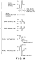
- Figure 14 shows a set of drive voltage signal waveforms used in the present invention.
- a scanning selection signal having alternating voltages ⁇ V S and a voltage O is applied to a scanning electrode, wherein the voltages ⁇ V S and the voltage O are values defined with reference to the voltage level of a scanning non-selection signal.
- the data electrodes are supplied with a black or white data signal depending on given data.
- the pixels on a scanning electrode supplied with a scanning selection signal are simultaneously erased into a black state in a period T1 during one scanning selection period, and then in a subsequent period T2, a pixel supplied with a data signal (B) is set to a black state and a pixel supplied with a data signal (W) is set to a white state.
- temperature compensation may be effected by modulating (changing) the length of one scanning selection period (1H) and the magnitude of a drive voltage peak value V OP (capable of writing in black or white) which is V OP1 or V OP2 giving a maximum value during the period T2.
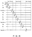
- FIG 15 is a waveform diagram showing an example of a sequence of applying a scanning selection signal shown in Figure 14 to the scanning electrodes.
- a scanning selection signal is sequentially applied to the scanning electrodes S1, S2, ... S F8+8(s-1) every 8th electrode (7 electrodes apart) in one vertical scanning (field scanning) and one picture is formed through 8 times of field scanning to complete one frame scanning.
- the scanning selection signal is also applied to the scanning electrodes S A and S B in the non-display region.
- the symbols F1, F2, ..., F8 each represent an ordinal number of field scanning in one frame scanning and the symbol s represents an ordinal number of scanning in one field scanning.
- a large-area liquid crystal cell particularly a ferroelectric liquid crystal cell realizing a high-contrast alignment state, while alleviating liquid crystal molecular movement or a local cell thickness change liable to occur in continual display of a fixed pattern and leading to inferior display quality, by disposing ridges or stripe conductor films in contact with transparent electrodes, respectively extending in ia certain direction.
- a liquid crystal cell is constituted by a pair of substrates respectively provided with scanning electrodes or data electrodes and uniaxial alignment axes which are substantially parallel with each other and substantially in the same direction, and a ferroelectric liquid crystal disposed between the substrates. At least one of the substrates is provided with ridges having a height at least one third of the spacing between the substrates or stripe transparent electrodes having thereon a stripe conductor film extending in the longitudinal direction of an associated one of the stripe transparent electrodes.
Landscapes
- Physics & Mathematics (AREA)
- Nonlinear Science (AREA)
- Chemical & Material Sciences (AREA)
- Crystallography & Structural Chemistry (AREA)
- General Physics & Mathematics (AREA)
- Optics & Photonics (AREA)
- Mathematical Physics (AREA)
- Liquid Crystal (AREA)
Applications Claiming Priority (4)
| Application Number | Priority Date | Filing Date | Title |
|---|---|---|---|
| JP10957691A JPH04317026A (ja) | 1991-04-16 | 1991-04-16 | 液晶セル |
| JP109576/91 | 1991-04-16 | ||
| JP261353/91 | 1991-09-13 | ||
| JP26135391A JPH0572536A (ja) | 1991-09-13 | 1991-09-13 | 強誘電性液晶表示素子 |
Publications (2)
| Publication Number | Publication Date |
|---|---|
| EP0509490A2 true EP0509490A2 (de) | 1992-10-21 |
| EP0509490A3 EP0509490A3 (en) | 1993-05-26 |
Family
ID=26449310
Family Applications (1)
| Application Number | Title | Priority Date | Filing Date |
|---|---|---|---|
| EP19920106552 Ceased EP0509490A3 (en) | 1991-04-16 | 1992-04-15 | Liquid crystal apparatus |
Country Status (2)
| Country | Link |
|---|---|
| US (1) | US5541752A (de) |
| EP (1) | EP0509490A3 (de) |
Cited By (3)
| Publication number | Priority date | Publication date | Assignee | Title |
|---|---|---|---|---|
| EP0571955A1 (de) * | 1992-05-26 | 1993-12-01 | Canon Kabushiki Kaisha | Flüssigkristallzusammensetzung und -vorrichtung |
| EP0795774A3 (de) * | 1996-03-11 | 1998-03-25 | Canon Kabushiki Kaisha | Flüssigkristallvorrichtung und deren Herstellungsverfahren |
| EP0584963B1 (de) * | 1992-07-30 | 2001-10-04 | Canon Kabushiki Kaisha | Flüssigkristall-Anzeigevorrichtung |
Families Citing this family (7)
| Publication number | Priority date | Publication date | Assignee | Title |
|---|---|---|---|---|
| JP3093627B2 (ja) * | 1996-02-09 | 2000-10-03 | キヤノン株式会社 | 液晶表示装置の製造方法 |
| JPH11100577A (ja) * | 1997-07-31 | 1999-04-13 | Canon Inc | 液晶の配向方法、液晶素子の製造方法、該製造方法により得られる液晶素子、液晶装置 |
| US6195147B1 (en) | 1997-08-01 | 2001-02-27 | Canon Kabushiki Kaisha | Liquid crystal substrate with optical modulation region having different alignment control forces |
| JP3957430B2 (ja) * | 1998-09-18 | 2007-08-15 | シャープ株式会社 | 液晶表示装置 |
| JP3323847B2 (ja) * | 1999-02-22 | 2002-09-09 | キヤノン株式会社 | 電子放出素子、電子源および画像形成装置の製造方法 |
| US7416010B2 (en) * | 2002-03-08 | 2008-08-26 | Lg Display Co., Ltd. | Bonding apparatus and system for fabricating liquid crystal display device |
| JP6900279B2 (ja) | 2016-09-13 | 2021-07-07 | キヤノン株式会社 | トナー及びトナーの製造方法 |
Family Cites Families (32)
| Publication number | Priority date | Publication date | Assignee | Title |
|---|---|---|---|---|
| US4763995A (en) * | 1983-04-28 | 1988-08-16 | Canon Kabushiki Kaisha | Spacers with alignment effect and substrates having a weak alignment effect |
| US4715688A (en) * | 1984-07-04 | 1987-12-29 | Seiko Instruments Inc. | Ferroelectric liquid crystal display device having an A.C. holding voltage |
| JPS60156043A (ja) * | 1984-01-23 | 1985-08-16 | Canon Inc | カイラルスメクティック液晶素子 |
| JPS60188925A (ja) * | 1984-03-09 | 1985-09-26 | Canon Inc | 光学変調素子の製造法 |
| JPS60220316A (ja) * | 1984-04-16 | 1985-11-05 | Canon Inc | 液晶光学素子 |
| US4682858A (en) * | 1984-08-20 | 1987-07-28 | Canon Kabushiki Kaisha | Liquid crystal device having reduced-pressure region in communication with ferroelectric liquid crystal |
| JPS6167829A (ja) * | 1984-09-11 | 1986-04-08 | Canon Inc | カイラルスメクティック液晶素子 |
| JPS6186732A (ja) * | 1984-10-04 | 1986-05-02 | Canon Inc | 液晶装置 |
| US4712877A (en) * | 1985-01-18 | 1987-12-15 | Canon Kabushiki Kaisha | Ferroelectric display panel of varying thickness and driving method therefor |
| US4707078A (en) * | 1985-04-26 | 1987-11-17 | American Telephone And Telegraph Company, At&T Bell Laboratories | Ferroelectric liquid crystal devices using field-stabilized states |
| JPS61260222A (ja) * | 1985-05-15 | 1986-11-18 | Canon Inc | 液晶素子 |
| US4775225A (en) * | 1985-05-16 | 1988-10-04 | Canon Kabushiki Kaisha | Liquid crystal device having pillar spacers with small base periphery width in direction perpendicular to orientation treatment |
| US4778259A (en) * | 1985-07-17 | 1988-10-18 | Canon Kabushiki Kaisha | Ferroelectric liquid crystal devices having reverse twist angle and stable states resulting from A.C. excitation |
| JPS6232424A (ja) * | 1985-08-05 | 1987-02-12 | Canon Inc | 液晶装置 |
| DE3630012A1 (de) * | 1985-09-04 | 1987-04-23 | Canon Kk | Ferroelektrische fluessigkristallvorrichtung |
| JPH0685032B2 (ja) * | 1985-10-17 | 1994-10-26 | キヤノン株式会社 | カイラルスメクティック液晶素子 |
| JPS62119521A (ja) * | 1985-11-19 | 1987-05-30 | Canon Inc | 光学変調装置 |
| JP2654940B2 (ja) * | 1985-12-24 | 1997-09-17 | キヤノン株式会社 | 電気光学素子の製造方法 |
| US4712874A (en) * | 1985-12-25 | 1987-12-15 | Canon Kabushiki Kaisha | Ferroelectric liquid crystal device having color filters on row or column electrodes |
| US4820026A (en) * | 1986-03-20 | 1989-04-11 | Canon Kabushiki Kaisha | Ferroelectric liquid crystal device with modified polyvinyl alcohol alignment film |
| US4796980A (en) * | 1986-04-02 | 1989-01-10 | Canon Kabushiki Kaisha | Ferroelectric liquid crystal optical modulation device with regions within pixels to initiate nucleation and inversion |
| US4796979A (en) * | 1986-04-07 | 1989-01-10 | Canon Kabushiki Kaisha | Ferroelectric liquid crystal device having dual laminated alignment films |
| US4824218A (en) * | 1986-04-09 | 1989-04-25 | Canon Kabushiki Kaisha | Optical modulation apparatus using ferroelectric liquid crystal and low-resistance portions of column electrodes |
| JPS62280721A (ja) * | 1986-05-29 | 1987-12-05 | Matsushita Electric Ind Co Ltd | 強誘電性液晶表示パネル |
| JP2505756B2 (ja) * | 1986-07-22 | 1996-06-12 | キヤノン株式会社 | 光学変調素子の駆動法 |
| US4900132A (en) * | 1987-04-13 | 1990-02-13 | Tektronix, Inc. | Chiral liquid crystal cell |
| US4859036A (en) * | 1987-05-15 | 1989-08-22 | Canon Kabushiki Kaisha | Device plate having conductive films selected to prevent pin-holes |
| US5000545A (en) * | 1987-05-28 | 1991-03-19 | Canon Kabushiki Kaisha | Liquid crystal device with metal electrode partially overlying transparent electrode |
| JP2770944B2 (ja) * | 1987-08-19 | 1998-07-02 | キヤノン株式会社 | 液晶素子 |
| US4932758A (en) * | 1987-09-17 | 1990-06-12 | Canon Kabushiki Kaisha | Ferroelectric smectic liquid crystal device having a bistable alignment state providing two stable orientation states |
| JPH01179915A (ja) * | 1988-01-11 | 1989-07-18 | Canon Inc | 液晶素子 |
| EP0444705B1 (de) * | 1990-03-02 | 1999-05-26 | Canon Kabushiki Kaisha | Flüssigkristallelement und Flüssigkristallvorrichtung, die dieses Element verwendet |
-
1992
- 1992-04-15 EP EP19920106552 patent/EP0509490A3/en not_active Ceased
-
1994
- 1994-08-01 US US08/284,051 patent/US5541752A/en not_active Expired - Fee Related
Cited By (5)
| Publication number | Priority date | Publication date | Assignee | Title |
|---|---|---|---|---|
| EP0571955A1 (de) * | 1992-05-26 | 1993-12-01 | Canon Kabushiki Kaisha | Flüssigkristallzusammensetzung und -vorrichtung |
| US5458804A (en) * | 1992-05-26 | 1995-10-17 | Canon Kabushiki Kaisha | Liquid crystal composition, liquid crystal device and liquid crystal apparatus |
| EP0584963B1 (de) * | 1992-07-30 | 2001-10-04 | Canon Kabushiki Kaisha | Flüssigkristall-Anzeigevorrichtung |
| EP0795774A3 (de) * | 1996-03-11 | 1998-03-25 | Canon Kabushiki Kaisha | Flüssigkristallvorrichtung und deren Herstellungsverfahren |
| US6320639B1 (en) | 1996-03-11 | 2001-11-20 | Canon Kabushiki Kaisha | Liquid crystal device and process for production thereof |
Also Published As
| Publication number | Publication date |
|---|---|
| US5541752A (en) | 1996-07-30 |
| EP0509490A3 (en) | 1993-05-26 |
Similar Documents
| Publication | Publication Date | Title |
|---|---|---|
| US4941736A (en) | Ferroelectric liquid crystal device and driving method therefor | |
| US4744639A (en) | Ferroelectric liquid crystal device having a flattening layer | |
| US5612802A (en) | Chiral smectic liquid crystal device having alignment film over electrodes being different and having different pretilt from alignment film between electrodes | |
| US6317111B1 (en) | Passive matrix addressed LCD pulse modulated drive method with pixel area and/or time integration method to produce covay scale | |
| US4765720A (en) | Method and apparatus for driving ferroelectric liquid crystal, optical modulation device to achieve gradation | |
| US5092665A (en) | Driving method for ferroelectric liquid crystal optical modulation device using an auxiliary signal to prevent inversion | |
| EP1042702B1 (de) | Bistabile nematische flüssigkristallvorrichtung | |
| EP0240010A1 (de) | Optische Modulationsvorrichtung | |
| KR0125785B1 (ko) | 액정 소자 | |
| US5559616A (en) | Driving method for ferroelectric liquid crystal device with partial erasure and partial writing | |
| US5500749A (en) | Ferroelectric liquid crystal element with an AC holding voltage below the level at which the molecules migrate | |
| US5189535A (en) | Liquid crystal display element and method for driving same | |
| US5541752A (en) | Liquid crystal apparatus | |
| US6320571B1 (en) | Bistable liquid crystal display device | |
| EP0542518B1 (de) | Flüssigkristallelement und Steuerverfahren dafür | |
| US5661532A (en) | Chiral smectic liquid crystal device | |
| US5276542A (en) | Ferroelectric liquid crystal apparatus having temperature compensation control circuit | |
| US5204766A (en) | Ferroelectric liquid crystal cell with particulate adhesive density higher near side | |
| US5452114A (en) | Ferroelectric liquid crystal device with grooves between electrode on one substrate, ridges on the other | |
| EP0500070B1 (de) | Flüssigkristallvorrichtung | |
| EP0782123A1 (de) | Flüssigkristalleinrichtung und Steuerverfahren zur Verhinderung des Vergelbungsphänomens | |
| US6304310B1 (en) | Liquid crystal apparatus | |
| JP2517549B2 (ja) | 光学変調素子 | |
| CA1258327A (en) | Driving method for optical modulation device | |
| JP3219709B2 (ja) | 液晶素子、液晶装置、及び液晶素子の駆動方法 |
Legal Events
| Date | Code | Title | Description |
|---|---|---|---|
| PUAI | Public reference made under article 153(3) epc to a published international application that has entered the european phase |
Free format text: ORIGINAL CODE: 0009012 |
|
| 17P | Request for examination filed |
Effective date: 19920415 |
|
| AK | Designated contracting states |
Kind code of ref document: A2 Designated state(s): AT BE CH DE DK ES FR GB GR IT LI LU NL PT SE |
|
| PUAL | Search report despatched |
Free format text: ORIGINAL CODE: 0009013 |
|
| AK | Designated contracting states |
Kind code of ref document: A3 Designated state(s): AT BE CH DE DK ES FR GB GR IT LI LU NL PT SE |
|
| 17Q | First examination report despatched |
Effective date: 19950227 |
|
| STAA | Information on the status of an ep patent application or granted ep patent |
Free format text: STATUS: THE APPLICATION HAS BEEN REFUSED |
|
| 18R | Application refused |
Effective date: 19980202 |