EP0503961B1 - Méthode pour la fabrication d'un substrat en verre pour disque - Google Patents
Méthode pour la fabrication d'un substrat en verre pour disque Download PDFInfo
- Publication number
- EP0503961B1 EP0503961B1 EP92302183A EP92302183A EP0503961B1 EP 0503961 B1 EP0503961 B1 EP 0503961B1 EP 92302183 A EP92302183 A EP 92302183A EP 92302183 A EP92302183 A EP 92302183A EP 0503961 B1 EP0503961 B1 EP 0503961B1
- Authority
- EP
- European Patent Office
- Prior art keywords
- glass substrate
- fabricating
- substrate
- guide track
- area
- Prior art date
- Legal status (The legal status is an assumption and is not a legal conclusion. Google has not performed a legal analysis and makes no representation as to the accuracy of the status listed.)
- Expired - Lifetime
Links
Images


Classifications
-
- G—PHYSICS
- G11—INFORMATION STORAGE
- G11B—INFORMATION STORAGE BASED ON RELATIVE MOVEMENT BETWEEN RECORD CARRIER AND TRANSDUCER
- G11B7/00—Recording or reproducing by optical means, e.g. recording using a thermal beam of optical radiation by modifying optical properties or the physical structure, reproducing using an optical beam at lower power by sensing optical properties; Record carriers therefor
- G11B7/24—Record carriers characterised by shape, structure or physical properties, or by the selection of the material
- G11B7/26—Apparatus or processes specially adapted for the manufacture of record carriers
- G11B7/261—Preparing a master, e.g. exposing photoresist, electroforming
Definitions
- the present invention relates to a method of fabricating a glass substrate for, or for use in the manufacture of, an optical recording medium.
- the optical memory medium can be classified into a read-only memory, a write-once memory and a rewritable memory according to its working form.
- the optical memory medium to be used as the write-once memory and rewritable memory uses a substrate for a disk.
- the substrate for a disk preliminarily comprises on a glass substrate guide tracks for guiding optical beams for recording, reading and erasing information to predetermined positions on the optical memory element, and track addresses for identifying track numbers.
- the track is divided into a plurality of sectors. In the case where information should be managed, sector addresses and the like are often provided in advance. As shown in Fig.
- the depth of a guide track portion 1b is not equal to that of a sector (or track) address portion 1a, and the address portion 1a is provided between the guide track portions 1b.
- the depth of the guide track portion approximates ⁇ / (8 x n) and the depth of the address portion approximates ⁇ / (4 x n) (where ⁇ is a wavelength of light to be used and n is a refractive index of a substrate).
- ⁇ is a wavelength of light to be used and n is a refractive index of a substrate.
- a photomask is used for forming a glass substrate for a disk by the contact printing method and the dry etching method.
- the photomask has such a shape that a quantity of light radiated onto the guide track portion and sector (or track) address portion on a photoresist film is varied. This technique will be summarized with reference to Figs. 9 to 13.
- a positive type photoresist film 2 is provided on a glass substrate 1, and prebaking is then carried out.
- a photomask 3 having a thin film 4 for a mask is caused to contact the photoresist film 2 through the thin film 4.
- the thin film 4 is not provided in a formation area A1 of a sector (or track) address portion 1a. Consequently, a quantity of transmitted light is not reduced.
- the thin film 4 remains at a thickness of about 10 to 200 ⁇ in a formation area B1 of a guide track portion 1b. Consequently, a quantity of transmitted light in the formation area B1 is smaller than in the formation area A1.
- ultraviolet rays 5 are radiated to expose the photoresist film 2 provided below the photomask 3 (see Fig. 10). Thereafter, the photomasks 3 and 4 are removed.
- the photoresist film 2 thus exposed is developed, and postbaking is then carried out. Exposure is fully carried out by strong light in a formation area A2 of the address portion 1a on the photoresist film 2. Consequently, the photoresist film 2 is completely developed so that the glass substrate 1 appears. In a formation area B2 of the guide track portion 1b on the photoresist film 2, the exposure is carried out by weaker light than in the formation area A2. Consequently, development is stopped halfway. As a result, the photoresist film 2 remains by a thickness according to a quantity of transmitted light in the formation area B1 on the thin film 4, so that the glass substrate 1 does not appear.
- the reference numeral 22a denotes a residual photoresist film.
- the glass substrate 1 is subjected to dry etching using gas such as CF 4 or CHF 3 .
- the photoresist film 2 shown in Fig. 11 is also etched simultaneously. Consequently, when etching is started, the etching of the glass substrate 1 is advanced in the formation area A2 so that a deep pit 11a is formed on the glass substrate 1.
- the residual photoresist film 22a is etched in the formation area B2.
- the etching of the glass substrate 1 is advanced. Consequently, there is formed a groove 11b which is shallower than the pit 11a in the formation area A2.
- the reference numeral 22b denotes a photoresist film which remains when the etching is completed.
- the photoresist film 22b remaining on the glass substrate 1 is removed to form on the glass substrate 1 the address portion 1a as a deep pit 111 and the guide track portion 1b as a shallow groove 112.
- the address portion 1a and guide track portion 1b have different depths.
- the depth of the groove 112 forming the guide track portion 1b is defined by the thickness of the photoresist film 22a remaining on the guide track portion 1b, and the etching speeds of the photoresist film 1 including the residual photoresist film 22a and the glass substrate 1 as shown in Fig. 11.
- the thickness of the photoresist film 22a is defined by a quantity of transmitted light and developing conditions in the guide track portion 1b. Accordingly, it is difficult to uniformly form pits and grooves with good reproducibility.
- EP-A-0 241 028 discloses a process of forming grooves of different depths in a glass substrate in the manufacture of an optical memory disc. The process corresponds to that described above with reference to Figs. 9 to 13.
- the present invention provides a method of fabricating a glass substrate, as defined by claim 1.
- a method of manufacturing an optical recording medium is defined by claim 11 or claim 12.
- a glass substrate fabricated according to the method of the present invention is used as a substrate for an optical memory medium or as a substrate for a master plate for preparing a stamper to be used for injection molding.
- a photoresist film 2 on a glass substrate 1 is exposed (see Fig. 2). Then, development is carried out so that the surface of the glass substrate 1 appears in an address portion formation area A2 and the photoresist film 2 remains as a first residual film 6 on the surface of the glass substrate 1 in a guide track portion formation area B2 as shown in Fig. 3.
- exposure is carried out by radiating ultraviolet rays 5 onto the photoresist film 2 with the use of photomasks 3 and 4, or by a laser cutting method using laser beams.
- the photomasks 3 and 4 can completely remove the photoresist film 2 in the address portion formation area and can stop the removal of the photoresist film 2 halfway in the guide track portion formation area (see Fig. 2)
- the photomasks 3 and 4 are preferably composed of a quartz substrate 3 and a metallic pattern 4 such as tantalum (Ta), chromium (Cr) or titanium (Ti) which is formed on the quartz substrate 3.
- a metallic pattern 4 such as tantalum (Ta), chromium (Cr) or titanium (Ti) which is formed on the quartz substrate 3.
- Ar ion laser beams having a large quantity of light for exposing the address portion formation area and Ar ion laser beams having a small quantity of light for exposing the guide track portion formation area are radiated onto a photoresist plane, and scan the photoresist plane while rotating the glass substrate so that each formation area is exposed like spirals.
- the glass substrate 1 which includes the photoresist film 2 having the first residual film 6 is subjected to first etching. Consequently, the glass substrate 1 in an address portion formation area A3 is sunk by a predetermined thickness. In a guide track portion formation area B3, the first residual film 6 is removed to cause a second residual film 7 to remain (see Fig. 4).
- the first etching is a known method, for example, dry etching carried out at a power of 1500 W and a pressure of 12 mTorr in a plasma atmosphere using gas such as CF 4 or CHF 3 .
- the second residual film 7 is removed by first ashing so as to cause the surface of the glass substrate 1 to appear in a guide track portion formation area B4 (see Fig. 5).
- the first ashing serves to remove an organic material such as a photoresist film.
- the second residual film 7 can be removed without depending on the non-uniformity of thickness distribution of the first and second residual films 6 and 7. Consequently, the surface of the glass substrate 1 can completely appear in the guide track portion formation area B4. More specifically, the glass substrate 1 cannot be removed by the first ashing. Accordingly, pits in an address portion formation area A4 can be defined only by the first etching without depending on the selection ratio of the glass substrate to the photoresist film (for example, 1 : 1 or 1 : 2), and the thicknesses of the first and second residual films 6 and 7.
- the first ashing is a known method, for example, plasma etching carried out at a power of 200 W and a pressure of 10 to 50 mTorr in an oxygen plasma atmosphere.
- second etching is carried out to sink by a predetermined thickness the glass substrate 1 which is caused to appear by the first ashing. Consequently, there is formed a shallow groove as a guide track portion 1b in the guide track portion formation area B4.
- the glass substrate 1 is sunk by a predetermined thickness in the address portion formation area A3 so as to form a deep pit as an address portion 1a (see Fig. 6).
- the glass substrate 1 is sunk by the second etching. More specifically, the guide track portion 1b can be defined only by the second etching without depending on the selection ratio of the glass substrate to the photoresist film, and the thicknesses of the first and second residual films 6 and 7. At this time, the address portion 1a forms a pit having a desired depth by the first and second etching.
- a third residual film 8 (see Fig. 6) provided between the address portion formation area A4 and the guide track portion formation area B4 is removed by second ashing.
- the depths of the address portion 1a and guide track portion 1b are not affected by the second ashing.
- the depths of the guide track portion and address portion can be defined only by the first and second etching without depending on the selection ratio of the glass substrate to the photoresist film, and the thicknesses of the first and second residual films. Consequently, the guide track portion and address portion can have grooves and pits uniformly formed on the glass substrate with good reproducibility.
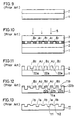
- FIG. 1 to 7 show fabricating steps according to the present invention.
- a positive type photoresist film 2 is provided on a glass substrate 1 as a glass substrate for a disk. Then, prebaking is carried out.
- a photomask 3 is caused to contact the photoresist film 2 through a thin film 4 for a mask.
- Ultraviolet rays 5 are radiated onto the photomask 3 so as to expose the photoresist film 2.
- the thin film 4 is not provided in a formation area A1 of a sector (or track) address portion 1a. Consequently, a quantity of light transmitted to the photoresist film 2 is not reduced.
- the thin film 4 remains at a thickness of about 10 to 200 ⁇ in a formation area B1 of a guide track portion 1b. Consequently, the quantity of light transmitted to the photoresist film 2 is reduced.
- the exposed photoresist film 2 is developed as shown in Fig. 3. Then, postbaking is carried out. A formation area A2 of the address portion 1a on the photoresist film 2 is fully exposed by strong light. Consequently, the photoresist film 2 is completely developed so that the glass substrate 1 appears. A formation area B2 of the guide track portion 1b on the photoresist film 2 is exposed by weaker light than in the formation area A2 of the address portion 1a. Consequently, the development of the photoresist film 2 is stopped halfway. The photoresist film 2 in the formation area B2 of the guide track portion 1b remains as a first residual film 6. The first residual film 6 is formed at a thickness according to a quantity of transmitted light in the formation area B1. The above-mentioned steps are the same as those of the prior art.
- the glass substrate 1 including the photoresist film 2 is entirely etched as shown in Fig. 4. Consequently, the glass substrate 1 in a formation area A3 of the address portion 1a and the first residual film 6 in a formation area B3 of the guide track portion 1b are simultaneously etched by a thickness of 200 to 800 ⁇ . In this case, the first residual film 6 in the formation area B3 is not completely removed so as to remain as a second residual film 7.
- the second residual film 7 in the formation area B3 of the guide track portion 1b is removed by ashing (first ashing). Consequently, the glass substrate 1 in the formation area B3 of the guide track portion 1b appears (see Fig. 5). In this case, the glass substrate 1 in the formation area A3 which has appeared is not removed. In this state, the glass substrate 1 appears in formation areas A4 and B4. The glass substrate 1 in other areas is covered by the photoresist film 2.
- the glass substrate 1 including the photoresist film 2 is entirely etched (second etching). Consequently, a portion in which the glass substrate 1 appears, i.e., the glass substrate 1 in the formation areas A4 and B4 of the address portion 1a and guide track portion 1b is also etched by a thickness of 300 to 1000 ⁇ (see Fig. 6). In this case, the photoresist film 2 is removed by a thickness of about 300 to 1000 ⁇ so as to remain as a third residual film 8.
- the third residual film 8 is removed by ashing (second ashing). Consequently, there is formed a glass substrate 5 for a disk having address portions 1a and guide track portions 1b of which pits and grooves have different depths.
- the pit of the address portion 1a has a depth of 1400 ⁇
- the groove of the guide track portion 1b has a depth of 700 ⁇ .
- These depths are set to ⁇ / 8n in the guide track portion 1b and ⁇ / 4n in the address portion 1a (where ⁇ is a wavelength of a laser beam radiated onto the glass substrate 5 and n is a refractive index of a substrate).
- a new etching process is incorporated. Consequently, the depths of the pit and groove of the address portion and guide track portion are defined only by etching.
- the address and guide track portions include pits and grooves which have different depths, respectively.
Landscapes
- Engineering & Computer Science (AREA)
- Manufacturing & Machinery (AREA)
- Manufacturing Optical Record Carriers (AREA)
- Drying Of Semiconductors (AREA)
Claims (12)
- Procédé de fabrication d'un substrat de verre (1), pour un support d'enregistrement optique ou pour utilisation dans la fabrication de ce dernier, le substrat portant deux types de motifs (1a, 1b) se distinguant au moins par une épaisseur différente du substrat, le procédé comprenant une première étape de gravure, dans laquelle la surface du substrat est initialement exposée au niveau d'une première zone, dans laquelle un motif (1a) doit être formé, et est recouverte d'une couche de résist (6) au niveau d'une deuxième zone, où l'autre motif (1b) doit être formé, caractérisé en ce que, dans la première étape de gravure, le substrat est gravé uniquement au niveau de ladite première zone ; par une étape consistant à enlever la couche de résist restante (7) dans ladite deuxième zone après la première étape de gravure, de façon à exposer le substrat se trouvant dans la deuxième zone ; et par une deuxième étape de gravure, au cours de laquelle le substrat est soumis à une nouvelle gravure au niveau de ladite première zone pour parachever la formation de l'un des motifs (1a) et est soumis à une gravure au niveau de la deuxième zone pour former l'autre motif (1b).
- Procédé de fabrication d'un substrat de verre selon la revendication 1, dans lequel lesdits deux types de motifs sont constitués de portions (1b) de piste pilote et de portions (1a) d'adresse de secteur ou de piste ayant différentes profondeurs respectivement de sillons et de cratères, le procédé comprenant les étapes consistant :i) à former un film de photorésist (2) sur le substrat (1) ;ii) à procéder à une exposition (3, 4, 5) pour définir une pluralité de zones (B1) de formation de portions de piste pilote et de zones (A1) de formation de portions d'adresse de secteur ou de piste, intercalées entre des zones contiguës de formation de portions de piste pilote, et à mettre en oeuvre un développement, l'exposition amenant le substrat de verre, après développement, à apparaître dans la zone (A2) de formation des portions d'adresse, et amenant le film de photorésist à rester en tant que premier film résiduel (6) dans la zone (B2) de formation des portions de piste pilote;iii) à mettre en oeuvre ladite première étape de gravure pour graver le substrat de verre dans la zone (A3) de formation de portions d'adresse, sur une épaisseur prédéterminée de façon à former un cratère (la) et à enlever une portion de couche superficielle du premier film résiduel (6) de façon à former un deuxième film résiduel (7) ;iv) à réaliser un premier polissage pour éliminer le deuxième film résiduel (7), de façon que le substrat de verre apparaisse dans la zone (B4) de formation des portions de piste pilote ;v) à mettre en oeuvre ladite deuxième étape de gravure pour former un sillon (1b) dans la zone (B4) de formation de portions de piste pilote, et pour graver plus avant ledit cratère dans la zone (A4) de formation de portions d'adresse, de façon à former un cratère (1a) plus profond ; etvi) à mettre en oeuvre un deuxième polissage, pour enlever un troisième film de photorésist résiduel (8) qui reste sur le film de photorésist entre le cratère plus profond (1a) et le sillon (1b) après la deuxième étape de gravure.
- Procédé de fabrication d'un substrat de verre selon la revendication 2, dans lequel le premier et le deuxième polissages sont mis en oeuvre au moyen d'un appareil de gravure du type à plaques parallèles, qui est utilisé pour la première et la deuxième étapes de gravure.
- Procédé de fabrication d'un substrat de verre selon la revendication 2, dans lequel le premier et le deuxième polissages sont effectués dans une atmosphère de plasma à l'oxygène.
- Procédé de fabrication d'un substrat de verre selon la revendication 2, dans lequel la première et la deuxième gravures sont réalisées dans une atmosphère de plasma en utilisant un gaz tel que CF4 ou CHF3.
- Procédé de fabrication d'un substrat de verre selon l'une quelconque des revendications 2 à 5, dans lequel l'exposition est réalisée à l'aide d'un photomasque (3, 4) capable d'enlever complètement le film de photorésist (2) dans la zone (A1) de formation des portions d'adresse de secteur ou de piste, et d'arrêter l'enlèvement du film de photorésist (2) à mi-chemin dans la zone (B1) de formation des portions de piste pilote.
- Procédé de fabrication d'un substrat de verre selon la revendication 6, dans lequel le photomasque comprend un substrat de quartz (3) et un motif en métal (4) tel que le tantale, le chrome ou le titane, qui est formé sur le substrat de quartz.
- Procédé de fabrication d'un substrat de verre selon l'une quelconque des revendications 2 à 5, dans lequel l'exposition est réalisée par un procédé de coupage au laser utilisant deux faisceaux laser à ion Ar.
- Procédé de fabrication d'un substrat de verre selon l'une quelconque des revendications 1 à 8, dans lequel le substrat de verre est utilisé comme substrat pour ledit support d'enregistrement optique.
- Procédé de fabrication d'un substrat de verre selon l'une quelconque des revendications 1 à 8, dans lequel le substrat de verre est utilisé comme substrat pour une plaque maîtresse destinée à préparer un poinçon à utiliser pour un moulage par injection.
- Procédé de fabrication d'un support d'enregistrement optique, qui comprend le procédé de fabrication d'un substrat de verre en tant que substrat pour ledit support selon la revendication 9.
- Procédé de fabrication d'un support d'enregistrement optique, qui comprend le procédé de fabrication d'un substrat de verre en tant que plaque maîtresse selon la revendication 10.
Applications Claiming Priority (2)
| Application Number | Priority Date | Filing Date | Title |
|---|---|---|---|
| JP3051324A JPH04286736A (ja) | 1991-03-15 | 1991-03-15 | 光メモリ素子のマスター原盤用基板の製造方法 |
| JP51324/91 | 1991-03-15 |
Publications (3)
| Publication Number | Publication Date |
|---|---|
| EP0503961A2 EP0503961A2 (fr) | 1992-09-16 |
| EP0503961A3 EP0503961A3 (en) | 1992-11-25 |
| EP0503961B1 true EP0503961B1 (fr) | 1997-05-14 |
Family
ID=12883742
Family Applications (1)
| Application Number | Title | Priority Date | Filing Date |
|---|---|---|---|
| EP92302183A Expired - Lifetime EP0503961B1 (fr) | 1991-03-15 | 1992-03-13 | Méthode pour la fabrication d'un substrat en verre pour disque |
Country Status (6)
| Country | Link |
|---|---|
| US (1) | US5246531A (fr) |
| EP (1) | EP0503961B1 (fr) |
| JP (1) | JPH04286736A (fr) |
| KR (1) | KR950001879B1 (fr) |
| CA (1) | CA2062840C (fr) |
| DE (1) | DE69219652T2 (fr) |
Families Citing this family (19)
| Publication number | Priority date | Publication date | Assignee | Title |
|---|---|---|---|---|
| FR2701152B1 (fr) * | 1993-02-03 | 1995-03-10 | Digipress Sa | Procédé de fabrication d'un disque maître pour la réalisation d'une matrice de pressage notamment de disques optiques, matrice de pressage obtenue par ce procédé et disque optique obtenu à partir de cette matrice de pressage. |
| FR2702077B1 (fr) * | 1993-02-22 | 1995-04-21 | Digipress Sa | Procédé de fabrication d'un disque maître et d'une matrice de pressage de disques optiques perfectionnés, disque optique obtenu à partir de ce disque maître ou de cette matrice de pressage. |
| FR2716563B1 (fr) * | 1994-02-21 | 1996-06-07 | Digipress Sa | Substrat préformaté, substrat préformaté comportant des informations à dupliquer, leurs procédés de fabrication et procédé de fabrication d'un disque maître et/ou d'un disque optique. |
| US5783371A (en) * | 1994-07-29 | 1998-07-21 | Trustees Of Boston University | Process for manufacturing optical data storage disk stamper |
| US5503963A (en) * | 1994-07-29 | 1996-04-02 | The Trustees Of Boston University | Process for manufacturing optical data storage disk stamper |
| WO1996028396A1 (fr) * | 1995-03-13 | 1996-09-19 | Dsm N.V. | Composition de revetement de fibre optique, durcissable au rayonnement |
| US6287663B1 (en) * | 1995-10-31 | 2001-09-11 | Kabushiki Kaisha Ohara | Glass-ceramic substrate for a magnetic information storage medium |
| US5910262A (en) * | 1997-02-06 | 1999-06-08 | International Business Machines Corporation | Method and tool for laser texturing of glass substrates |
| JP3938253B2 (ja) | 1997-12-26 | 2007-06-27 | 日本板硝子株式会社 | 樹脂正立等倍レンズアレイおよびその製造方法 |
| JP2000348388A (ja) | 1999-06-04 | 2000-12-15 | Sharp Corp | 光記録媒体 |
| US6733957B2 (en) | 2000-12-27 | 2004-05-11 | Victor Company Of Japan | Disk substrate and manufacturing method therefor, and disk manufactured by the disk substrate |
| EP1420929B1 (fr) * | 2001-08-30 | 2011-10-12 | Bayer Technology Services GmbH | Procede de fabrication de corps moules, en particulier de structures optiques, et leur utilisation |
| GB0204496D0 (en) * | 2002-02-26 | 2002-04-10 | Plasmon Ltd | Optical disc mastering |
| US20050040032A1 (en) * | 2003-08-18 | 2005-02-24 | Yuan-Chang Lai | Stamper forming method |
| KR100641006B1 (ko) * | 2004-11-04 | 2006-11-02 | 엘지.필립스 엘시디 주식회사 | 인쇄판 |
| JP4289342B2 (ja) * | 2004-11-22 | 2009-07-01 | 日本ビクター株式会社 | 光ディスク及びその製造方法 |
| KR101711646B1 (ko) * | 2009-12-11 | 2017-03-03 | 엘지디스플레이 주식회사 | 임프린트용 몰드의 제조방법 및 임프린트용 몰드를 이용한 패턴 형성방법 |
| JP5252507B2 (ja) * | 2009-12-17 | 2013-07-31 | 独立行政法人産業技術総合研究所 | インプリントリソグラフィ用モールド製作方法 |
| KR101726641B1 (ko) * | 2011-08-03 | 2017-04-26 | 엘지디스플레이 주식회사 | 인쇄판의 제조 방법 |
Family Cites Families (9)
| Publication number | Priority date | Publication date | Assignee | Title |
|---|---|---|---|---|
| JPS5965951A (ja) * | 1982-10-08 | 1984-04-14 | Toshiba Corp | 情報記憶媒体用原盤 |
| JPS6050733A (ja) * | 1983-08-31 | 1985-03-20 | Sony Corp | 光学式記録媒体及びその原盤の製造装置 |
| JPS60170045A (ja) * | 1984-02-13 | 1985-09-03 | Pioneer Electronic Corp | アドレス,案内溝付光デイスク製造方法 |
| DE3689593T2 (de) * | 1985-08-30 | 1994-06-16 | Sharp Kk | Element für optische Speicherung und Verfahren zu dessen Herstellung. |
| JPS62128944A (ja) * | 1985-11-27 | 1987-06-11 | Sharp Corp | 光メモリ素子 |
| JPS62241149A (ja) * | 1986-04-11 | 1987-10-21 | Sharp Corp | 光メモリ素子用フォトマスク及びその製造方法 |
| JPS63155445A (ja) * | 1986-12-19 | 1988-06-28 | Canon Inc | 情報記録原盤の製造方法 |
| JPS6486344A (en) * | 1987-09-29 | 1989-03-31 | Victor Company Of Japan | Information recording carrier and production thereof |
| JPH01150254A (ja) * | 1987-12-07 | 1989-06-13 | Sharp Corp | 光メモリ素子用フォトマスク及びその製造方法 |
-
1991
- 1991-03-15 JP JP3051324A patent/JPH04286736A/ja active Pending
-
1992
- 1992-03-11 KR KR1019920003964A patent/KR950001879B1/ko not_active IP Right Cessation
- 1992-03-11 US US07/849,503 patent/US5246531A/en not_active Expired - Lifetime
- 1992-03-12 CA CA002062840A patent/CA2062840C/fr not_active Expired - Fee Related
- 1992-03-13 DE DE69219652T patent/DE69219652T2/de not_active Expired - Lifetime
- 1992-03-13 EP EP92302183A patent/EP0503961B1/fr not_active Expired - Lifetime
Also Published As
| Publication number | Publication date |
|---|---|
| DE69219652T2 (de) | 1997-11-20 |
| DE69219652D1 (de) | 1997-06-19 |
| KR950001879B1 (ko) | 1995-03-04 |
| EP0503961A2 (fr) | 1992-09-16 |
| EP0503961A3 (en) | 1992-11-25 |
| CA2062840C (fr) | 1997-09-16 |
| JPH04286736A (ja) | 1992-10-12 |
| US5246531A (en) | 1993-09-21 |
| KR920018692A (ko) | 1992-10-22 |
| CA2062840A1 (fr) | 1992-09-16 |
Similar Documents
| Publication | Publication Date | Title |
|---|---|---|
| EP0503961B1 (fr) | Méthode pour la fabrication d'un substrat en verre pour disque | |
| US20040231531A1 (en) | Reverse Optical mastering for data storage disk stamper | |
| JP2582996B2 (ja) | フォトマスクの製造方法 | |
| JPH0638299B2 (ja) | 案内溝付光デイスクの製造方法 | |
| EP0241028B1 (fr) | Masque photographique utilisé pour la fabrication d'un disque d'enregistrement optique, procédé pour la fabrication de ce masque et procédé pour la fabrication du disque optique | |
| US20060073422A1 (en) | Portable conformable deep ultraviolet master mask | |
| EP0708439B1 (fr) | Procédé de fabrication de disque maítre pour un disque optique | |
| EP0552943B1 (fr) | Matrice pour dispositif de mémoire optique et son procédé de fabrication | |
| CA2056308C (fr) | Methode de fabrication de photomasques de memoire optique | |
| US20030003326A1 (en) | Recording medium and process for manufacturing the medium | |
| US20100059477A1 (en) | Formation of Deep Hollow Areas and use Thereof in the Production of an Optical Recording Medium | |
| JP3014065B2 (ja) | 光ディスク,ガラスマスタ,ガラススタンパ,ガラス基板,それらの製造方法 | |
| JP3230313B2 (ja) | 反応性イオンエッチングによるパターニング加工物の製造方法 | |
| JP3129419B2 (ja) | 光ディスク用ガラスマスタの製造方法及び光ディスク用ガラスマスタ | |
| JP2002015474A (ja) | 光ディスク原盤及び光ディスク基板の作製方法 | |
| JPH06212458A (ja) | 反応性イオンエッチングによるパターニング 加工物の製造方法 | |
| JP4668666B2 (ja) | 光情報記憶媒体用原盤の製造方法、光情報記憶媒体用スタンパの製造方法、スタンパ、光情報記憶媒体用成形基板の製造方法及び光情報記憶媒体用成形基板 | |
| JPH09297940A (ja) | スタンパの製造方法 | |
| JPH01150254A (ja) | 光メモリ素子用フォトマスク及びその製造方法 | |
| JPH0517542B2 (fr) | ||
| KR960008712A (ko) | 광디스크 제조용 유리기판 및 포토마스크의 제조방법 | |
| JPH02266356A (ja) | 光メモリ素子用フォトマスクの製造方法 | |
| JPS6266444A (ja) | 光メモリ素子用フオトマスク | |
| JP2003317325A (ja) | 光情報記録媒体及びその原盤の作成方法 | |
| JPH04285739A (ja) | 光ディスク基板 |
Legal Events
| Date | Code | Title | Description |
|---|---|---|---|
| PUAI | Public reference made under article 153(3) epc to a published international application that has entered the european phase |
Free format text: ORIGINAL CODE: 0009012 |
|
| AK | Designated contracting states |
Kind code of ref document: A2 Designated state(s): DE FR GB IT NL |
|
| PUAL | Search report despatched |
Free format text: ORIGINAL CODE: 0009013 |
|
| AK | Designated contracting states |
Kind code of ref document: A3 Designated state(s): DE FR GB IT NL |
|
| 17P | Request for examination filed |
Effective date: 19930208 |
|
| 17Q | First examination report despatched |
Effective date: 19950807 |
|
| GRAG | Despatch of communication of intention to grant |
Free format text: ORIGINAL CODE: EPIDOS AGRA |
|
| GRAH | Despatch of communication of intention to grant a patent |
Free format text: ORIGINAL CODE: EPIDOS IGRA |
|
| GRAH | Despatch of communication of intention to grant a patent |
Free format text: ORIGINAL CODE: EPIDOS IGRA |
|
| GRAA | (expected) grant |
Free format text: ORIGINAL CODE: 0009210 |
|
| AK | Designated contracting states |
Kind code of ref document: B1 Designated state(s): DE FR GB IT NL |
|
| ITF | It: translation for a ep patent filed |
Owner name: RACHELI & C. S.R.L. |
|
| REF | Corresponds to: |
Ref document number: 69219652 Country of ref document: DE Date of ref document: 19970619 |
|
| ET | Fr: translation filed | ||
| PLBE | No opposition filed within time limit |
Free format text: ORIGINAL CODE: 0009261 |
|
| STAA | Information on the status of an ep patent application or granted ep patent |
Free format text: STATUS: NO OPPOSITION FILED WITHIN TIME LIMIT |
|
| 26N | No opposition filed | ||
| REG | Reference to a national code |
Ref country code: GB Ref legal event code: IF02 |
|
| PGFP | Annual fee paid to national office [announced via postgrant information from national office to epo] |
Ref country code: IT Payment date: 20110322 Year of fee payment: 20 Ref country code: FR Payment date: 20110317 Year of fee payment: 20 Ref country code: NL Payment date: 20110321 Year of fee payment: 20 |
|
| PGFP | Annual fee paid to national office [announced via postgrant information from national office to epo] |
Ref country code: GB Payment date: 20110309 Year of fee payment: 20 Ref country code: DE Payment date: 20110309 Year of fee payment: 20 |
|
| REG | Reference to a national code |
Ref country code: DE Ref legal event code: R071 Ref document number: 69219652 Country of ref document: DE |
|
| REG | Reference to a national code |
Ref country code: DE Ref legal event code: R071 Ref document number: 69219652 Country of ref document: DE |
|
| REG | Reference to a national code |
Ref country code: NL Ref legal event code: V4 Effective date: 20120313 |
|
| REG | Reference to a national code |
Ref country code: GB Ref legal event code: PE20 Expiry date: 20120312 |
|
| PG25 | Lapsed in a contracting state [announced via postgrant information from national office to epo] |
Ref country code: DE Free format text: LAPSE BECAUSE OF EXPIRATION OF PROTECTION Effective date: 20120314 |
|
| PG25 | Lapsed in a contracting state [announced via postgrant information from national office to epo] |
Ref country code: GB Free format text: LAPSE BECAUSE OF EXPIRATION OF PROTECTION Effective date: 20120312 |