EP0503605B1 - Bipolarer Transistor vom isolierten Gatetyp mit Überspannungschutz - Google Patents
Bipolarer Transistor vom isolierten Gatetyp mit Überspannungschutz Download PDFInfo
- Publication number
- EP0503605B1 EP0503605B1 EP92104203A EP92104203A EP0503605B1 EP 0503605 B1 EP0503605 B1 EP 0503605B1 EP 92104203 A EP92104203 A EP 92104203A EP 92104203 A EP92104203 A EP 92104203A EP 0503605 B1 EP0503605 B1 EP 0503605B1
- Authority
- EP
- European Patent Office
- Prior art keywords
- semiconductor layer
- layer
- drain
- junction
- voltage
- Prior art date
- Legal status (The legal status is an assumption and is not a legal conclusion. Google has not performed a legal analysis and makes no representation as to the accuracy of the status listed.)
- Expired - Lifetime
Links
Images


Classifications
-
- H—ELECTRICITY
- H10—SEMICONDUCTOR DEVICES; ELECTRIC SOLID-STATE DEVICES NOT OTHERWISE PROVIDED FOR
- H10D—INORGANIC ELECTRIC SEMICONDUCTOR DEVICES
- H10D62/00—Semiconductor bodies, or regions thereof, of devices having potential barriers
- H10D62/10—Shapes, relative sizes or dispositions of the regions of the semiconductor bodies; Shapes of the semiconductor bodies
- H10D62/17—Semiconductor regions connected to electrodes not carrying current to be rectified, amplified or switched, e.g. channel regions
- H10D62/393—Body regions of DMOS transistors or IGBTs
-
- H—ELECTRICITY
- H10—SEMICONDUCTOR DEVICES; ELECTRIC SOLID-STATE DEVICES NOT OTHERWISE PROVIDED FOR
- H10D—INORGANIC ELECTRIC SEMICONDUCTOR DEVICES
- H10D12/00—Bipolar devices controlled by the field effect, e.g. insulated-gate bipolar transistors [IGBT]
- H10D12/411—Insulated-gate bipolar transistors [IGBT]
- H10D12/441—Vertical IGBTs
Definitions
- the present invention relates to an insulated gate type bipolar-transistor (hereafter referred to as "IGBT") integrating excess voltage protecting function or drain voltage fixing function.
- IGBT insulated gate type bipolar-transistor
- a high voltage can be induced on an inductive load or a floating inductance in the circuit due to abrupt variation of circuit current flowing through the circuit.
- This high voltage is applied to the power switching element as a spike voltage to cause fatigue or breakage of the power switching element.
- a voltage clamp circuit including a constant voltage diode based on the operation principle of avalanche breakdown for turning ON the constant voltage diode before breakdown occurs in the power switching element because of applied spike voltage and thus fixing the level of the spike voltage within a safe operation range, is employed.
- the constant voltage diode is externally connected between the drain and gate of the IGBT element.
- the constant voltage diode causes an increase in of the assembling cost and also increases the overall circuit dimension.
- It can form the constant voltage diode integrally with the IGBT element by depositing a polycrystalline silicon layer on the substrates formed thereon the IGBT element to form the constant diode therein.
- this increases the necessary number of photo-masks in the element fabrication process leading to an increase in the production cost.
- Japanese Patent Publication JP-A-181270 proposes a method for integrating the constant voltage diode, in which the constant voltage diode having an operational principle of avalanche breakdown is incorporated in the IGBT element so that the constant voltage diode is disposed between the drain and the source on the equivalent circuit.
- This method solves problems, such as narrowing of the chip area of the IGBT element.
- the proposed construction is shown in Fig. 6.
- the reference numeral 61 denotes a source electrode
- 62 denotes a drain electrode
- 63 denotes a gate electrode.
- the upper layer of a substrate is composed of an insulating gate of DSA (diffusion self-aligmeld) construction, p + base layer 65, n + source layer 66 and forms a p type channel immediately below the gate.
- the substrate has a npnp four layer structure including n + source layer 66, p + base layer 65, n - drain layer 67 and p + drain layer 64 between n + layer 68 and drain electrode 62.
- the p + drain layer 64 at the side of the drain electrode 62 is separated into respective small segments and arranged parallel in a honeycomb fashion.
- the diode has a portion 69 of n + layer projecting into the n - layer 67 to be positioned closer to the p + layer 65 to provide avalanche type diode characteristics and thus protect the IGBT element from excess voltage.
- n + layer 68 at the drain side of the substrate. Because of the presence of n + layer 68, hole injection from the drain side upon conducting the IGBT is restricted to make the ON voltage higher.
- the substrate structure becomes complicated and thereby increases costs for fabrication of the wafer and costs for production.
- Patent Abstracts of Japan, vol. 10, no. 129 (E-403) [2186], May 14, 1986, corresponding to JP-A-60 260 152 proposes the formation of a high speed MOS gate bipolar transistor according to a simple construction by a method wherein a reversely conductive high concentration region is formed selectively in a single conductive substrate, and a reversely conductive low concentration layer is formed on the whole surface.
- an N+ type layer to suppress implantation of holes is provided between a P + type substrate and an N- type layer.
- the N+ type layers thereof can be formed easily by adhering phosphorus, antimony, arsenic, etc. according to diffusion or the ion implantation method, etc. to the P+ type substrate, prior to growing the N- type layer.
- this construction implantation of unnecessary carriers is suppressed, and turn-off is performed at a high speed. Moreover, a difficulty in regard to the process as the usual method is reduced sharply.
- DE-A-3 519 389 discloses a MOSFET with alterable conductivity comprising a semiconductor substrate of a first conductivity type, a semiconductor layer of a second conductivity type formed on the substrate and having a high resistivity, a base layer of the first conductivity type created in the semiconductor layer, a source layer of the second conductivity type formed in the base layer, a gate electrode that is formed on a gate isolating layer that itself is formed on a channel zone that, on the other hand, is created in a surface of the base layer between the semiconductor layer and the base layer, a source electrode that is in ohmic contact with the source layer and the base layer, and a drain electrode that is formed on the surface of the semiconductor substrate opposite the semiconductor layer.
- This MOSFET is characterized in that its saturation current is smaller than a latch-up current when a predetermined gate voltage is applied to the gate electrode.
- an object of the present invention to provide an IGBT element that incorporates excess voltage protection and drain voltage fixing function in a monolithic structure with a function for clamping a drain-source voltage without causing an increase in the ON voltage.
- the present inventors propose a structure in which avalanche breakdown is suppressed within an IGBT element under a desired clamping condition of drain-source voltage and a minority carrier is injected from p + substrate to n - layer.
- n channel type IGBT an operation of a n channel type IGBT will be discussed such that the first conductivity type is a p type and the second conductivity type is a n type.
- a pn junction formed between the second n type semiconductor layer and the third p type semiconductor layer is in a reverse biased condition. Then, a depletion region propagates from this pn junction.
- the depletion region propagates within the second n type semiconductor layer toward the first p type semiconductor layer according to an increase of the voltage between the source electrode and the drain electrode.
- the depletion region When the depletion region reaches a pn junction formed between the first p type semiconductor layer and the second n type semiconductor layer, it reduces a potential barrier formed by diffusion potential at the pn junction. By this, from the first p type semiconductor layer to the second n type semiconductor layer, a hole as a minority carrier is injected. The hole flows through the void formed in the second n type semiconductor layer to reach the third p type semiconductor layer and then flows to the source electrode. Furthermore, the hole flows to the source electrode via the third p type semiconductor layer as a drift current because of the electric field within the depletion region.
- a current rapidly flows between the source electrode and the drain electrode to suppress an increase of the voltage between the source electrode and the drain electrode.
- This phenomenon is known as a punch through phenomenon in the bipolar-transistor to form a void in all regions of the base layer and create the current between the collector and emitter.
- the present invention applies this phenomenon to the IGBT.
- the voltage V DSP between the source electrode and the drain electrode, at which the current starts to flow is a charge voltage, at which the end of the depletion region reaches the first p type semiconductor layer through the second n type semiconductor layer. Therefore, the level of the voltage V DSP can be set by selecting the thickness and impurity concentration of the second n type semiconductor layer. Namely, by setting the thickness and impurity concentration of the second n type semiconductor layer so that the V DSP becomes within the safe operation region of the element (first feature), it becomes possible to protect the IGBT element from excess voltage.
- the source-drain voltage becomes fixed in the vicinity of a particular voltage.
- the function preventing the source-drain voltage from rising across a given voltage and, at the same time, fixing the voltage at a particular voltage range can be internally incorporated.
- an injection amount of carrier (hole) to be injected into the second n type semiconductor layer via the pn junction when the depletion region reaches the first p type semiconductor layer can be restricted and thus can restrict the formation of a conductivity modulated region and the reduction of resistance associated with injection of the hole.
- fluctuation of drain voltage because of conductivity modulation-caused by an injection of a minority carrier can be suppressed to make the drain voltage more stable upon starting the current flow through the element.
- the present invention by setting the impurity concentration and thickness of the second semiconductor layer at predetermined values, avalanche breakdown can be internally suppressed in the IGBT element at a desired condition corresponding to a desired clamp voltage between the drain and the source. Furthermore, since the invention injects a minority carrier from p + substrate to n - substrate, it becomes unnecessary to incorporate the constant voltage diode having an operation principle of avalanche breakdown. Therefore, the present invention can achieve a remarkable advantage in that the IGBT element incorporating excess voltage protection and a drain voltage fixing function in a monolithic structure with a function for clamping drain-source voltage without causing an increase in the ON voltage.
- Fig. 1 is a section of a unit cell and a guard ring of an IGBT. The structure will be discussed in order of fabrication.
- a p + drain layer 4 (first semiconductor layer) is prepared.
- a high resistance n - drain layer 3 (second semiconductor layer) is formed by growing monocrystalline silicon by way of vapor deposition or so forth.
- This n - drain layer 3 has a predetermined impurity concentration ND and a predetermined thickness t e , as set out later.
- a p type base layer 7 (third layer) and a p type layer 13 are formed simultaneously by way of selective diffusion.
- the p type layer 13 is a guard ring formed for providing high breakdown voltage.
- an n + source layer 8 (fourth layer) is formed by way of selective diffusion.
- the p type base layer and the n + type source layer 8 are self-alignment using DSA (Diffusion Self Alignment) technology using a gate electrode 10 formed on a gate oxide layer 11 formed by oxidation of the surface of the n - drain layer 3 as a mask, and thus forms a channel region.
- an interlayer insulation layer 12 is formed. Thereafter, to establish an ohmic contact formed between the p type base layer 7 and the n + source layer 8, contact holes are formed through the gate oxide layer and the interlayer insulation layer 12.
- a source electrode 9 and gate electrode pad (not shown) are formed. Then, a metal layer is deposited on the reverse side of the p + type drain layer 4 to form a drain electrode 1.
- the impurity concentration ND and the thickness t e from the lower surface of the p type base layer 7 of the n - drain layer 3 are set so that a depletion region propagates from the p type base layer 7 and reaches the p + type drain layer 4 through the n - drain layer 3 at a voltage smaller than an avalanche breakdown voltage of pn junction between the p type base layer 7 and the n - drain layer 3.
- the depletion region propagating from the p type base layer 7 reaches the p + drain layer at a voltage V DSP lower than a voltage V DSA at which an avalanche breakdown occurs in the element.
- the voltage V DSP to cause carrier injection from the p + drain layer 4 as the substrate can be set at 350V.
- the drain voltage fixing function can be realized.
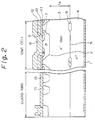
- Fig. 2 shows a section of a unit cell and a guard ring of an IGBT according to the present invention.
- the shown embodiment is differentiated from that illustrated in Fig. 1, in that an n + layer having a cyclic stripe pattern is provided in the vicinity of the pn junction 5 of the substrate.
- the n + layer 6 is formed at or in the vicinity the on junction 5 by selective diffusion of an impurity on the surface of the p + type drain layer 4, or, as an alternative, by forming a n - layer with a certain thickness on the surface of the p + type drain layer 4, subsequently performing selective diffusion of an impurity, and then performing the fabrication process discussed with respect to the Fig. 1.
- similar elements are represented by the same reference numerals as in Fig. 1.
- the depletion region When a positive voltage V D is applied to the drain electrode 1 while maintaining the potential at the source electrode 9 and the gate electrode 10 at the ground level, the depletion region is formed in n - type drain layer 3 because of reverse bias at the pn junction 2 between the p type base layer 7 and the n - drain layer 3.
- the depletion region propagates within the n - drain layer 3 toward the p + type drain layer 4 according to an increase in the voltage V D .
- the end of the depletion region reaches the position where the n + layer 6 is formed, propagation of the depletion region is blocked at the region where the n + layer 6 is selectively formed.
- the depletion region reaches the pn junction to reduce the potential barrier thereat to cause injection of a hole in substantially the same manner as that discussed in the first embodiment.
- the area to inject a hole can be restricted.
- the effect of this structure will be discussed in comparison with the structure that does not have the n + type layer 6.
- the depletion region when the depletion region reaches the p + type drain layer to start injection of a hole to the n - type drain layer 4, a region where the minority carrier is increased, is formed in the vicinity of pn junction 5 of the substrate.
- the conductivity is lowered (conductivity modulation) to cause a lowering of resistance between the source electrode and the drain electrode.
- the relationship between the drain current versus the drain voltage shows negative characteristics to decrease the drain voltage according to an increase in the drain current.
- the drain current is further increased, as propagation of the conductivity modulated region is restricted and thus the resistance between the source electrode and the drain electrode becomes fixed to cause an increase in the drain voltage again. Therefore, as shown in Fig. 3, the characteristics becomes I-V characteristics with a slight fluctuation of the drain voltage at the initiation of a current flow.
- the fluctuation of the drain voltage at the region of initiation of a flow of drain current is caused by a reduction of the element resistance due to the formation of the conductivity modulated region in the vicinity of the pn junction 5 by an injection of a minority carrier (hole) to the n - drain layer 3.
- the drain voltage will never fluctuate even at the initiation of a flow of the drain current, and thus can be stably fixed.
- n + type layer 6 is formed as a cyclic repeated pattern over the overall surface of the element, it becomes possible to make the current density flowing through the element uniform.
- Fig. 2 shows the example in which the n + type layer 6 is formed at the interface (pn junction 5) of the p + type drain layer 4 and the n - type drain layer 3, the equivalent effect can be obtained even when the n + type layer is formed at an upper or lower position from the interface surface of the p + type drain layer 4 and the n - type drain layer 3.
- the pattern of the n + type layer 6 is not specified as a stripe pattern but can be any pattern, such as a net pattern or so forth.
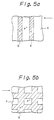
- Fig. 5 shows the section at pn junction 5
- Fig. 5(a) shows an embodiment where the n + type layer 6 is formed as a stripe pattern
- Fig. 5(b) shows an embodiment where the n + type layer 6 is formed as a net.
- n channel type IGBT in which the first conduction type is a p type and the second conductivity type is a n type
- the present invention is equally applicable for a p channel type IGBT, in which the conductivity types are reversed.
Landscapes
- Insulated Gate Type Field-Effect Transistor (AREA)
- Bipolar Transistors (AREA)
Claims (7)
- Bipolartransistor mit isoliertem Gate, welcher aufweist:dadurch gekennzeichnet, daß eine fünfte Halbleiterschicht (6) des zweiten Leitfähigkeitstyps bei oder in der Umgebung des ersten pn-Übergangs zwischen der ersten Halbleiterschicht (4) und der zweiten Halbleiterschicht (3) angeordnet ist, wobei die fünfte Halbleiterschicht (6) eine höhere Störstellenkonzentration als die zweite Halbleiterschicht (3) aufweist und ein eine Kontaktoberfläche zwischen der ersten und der zweiten Halbleiterschicht (3, 4) belassendes Muster aufweist, wodurch Ladungsträger hierdurch übertragen werden können.eine erste Halbleiterschicht (4) eines ersten Leitfähigkeitstyps;eine zweite Halbleiterschicht (3) eines zweiten Leitfähigkeitstyps, welche eine Grenzfläche mit der ersten Halbleiterschicht (4) und eine der Grenzfläche gegenüberliegende Hauptoberfläche aufweist, wobei an der Grenzfläche ein erster pn-Übergang ausgebildet ist;eine dritte Halbleiterschicht (7) des ersten Leitfähigkeitstyps, welche in der zweiten Halbleiterschicht (3) ausgebildet ist, wobei sie an die Hauptoberfläche anstößt und mit der zweiten Halbleiterschicht (3) einen zweiten pn-Übergang ausbildet, der an der Hauptoberfläche endet;eine vierte Halbleiterschicht (8) des zweiten Leitfähigkeitstyps, welche in der dritten Halbleiterschicht (7) ausgebildet ist, wobei sie an die Hauptoberfläche anstößt und mit der dritten Halbleiterschicht (7) einen dritten pn-Übergang ausbildet, der an der Hauptoberfläche endet;eine Gateelektrode (10), welche über eine Gateisolationsschicht (11) auf einer Kanalregion ausgebildet ist, die an die Oberfläche der dritten Halbleiterschicht (7) angrenzt, welche sich zwischen der zweiten Halbleiterschicht (3) und der vierten Halbleiterschicht (8) erstreckt;eine Sourceelektrode (9), welche sowohl die dritte als auch die vierte Halbleiterschicht (7 und 8) direkt berührt;eine Drainelektrode (1), welche die erste Halbleiterschicht (4) direkt berührt; wobeidie zweite Halbleiterschicht (3) eine derartige Störstellenkonzentration und eine derartige Dicke aufweist, daß eine Verarmungsregion, welche sich von dem zweiten Übergang zwischen der dritten Halbleiterschicht (7) und der zweiten Halbleiterschicht (3) aus in Richtung des Inneren der zweiten Halbleiterschicht (3) erstreckt, bei einer zwischen der Drainelektrode (1) und der Sourceelektrode (9) angelegten Spannung, die geringer ist als die Drain/Source-Spannung, bei welcher ein kritisches elektrisches Feld bei oder in der Umgebung der zweiten Halbleiterschicht (3) einen teilweisen Lawinendurchbruch hervorruft, die erste Halbleiterschicht (4) durch die zweite Halbleiterschicht (3) hindurch erreicht und Minoritätsladungsträger für die zweite Halbleiterschicht (3) von der ersten Halbleiterschicht (4) aus in die zweite Halbleiterschicht (3) injiziert werden und zu der Sourceelektrode (9) fließen;
- Bipolartransistor mit isoliertem Gate gemäß Anspruch 1, dadurch gekennzeichnet, daß das Muster der fünften Halbleiterschicht (6) ein sich wiederholendes Muster bei oder in der Umgebung der Grenzfläche zwischen der ersten und der zweiten Halbleiterschicht (4 und 3) aufweist.
- Bipolartransistor mit isoliertem Gate gemäß Anspruch 2, dadurch gekennzeichnet, daß das sich wiederholende Muster der fünften Halbleiterschicht (6) ein netzförmiges oder streifenförmiges Muster ist.
- Bipolartransistor mit isoliertem Gate gemäß Anspruch 1, dadurch gekennzeichnet, daß
die dritte Halbleiterschicht (7) eine höhere Störstellenkonzentration aufweist, wodurch ein abrupter pn-übergang mit der zweiten Halbleiterschicht (3) ausgebildet ist;
die vierte Halbleiterschicht (8) von der zweiten Halbleiterschicht (3) um einen gegebenen Abstand beabstandet ist; und
die Störstellenkonzentration ND der zweiten Halbleiterschicht (3) und eine Dicke te zwischen dem zweiten pn-Übergang zwischen der zweiten Halbleiterschicht (3) und der dritten Halbleiterschicht (7) und dem ersten pn-Übergang zwischen der zweiten Halbleiterschicht (3) und der ersten Halbleiterschicht (4) so bestimmt sind, daß eine durch die nachstehende Gleichung
VR eine Drain/Source-Spannung VR ist, die geringer als eine Spannung ist, welche an dem zweiten pn-Übergang zwischen der dritten Halbleiterschicht (7) und der zweiten Halbleiterschicht (3) einen Lawinendurchbruch hervorruft;
ε0 die elektrische Feldkonstante im Vakuum ist; und
q die Elementarladung ist. - Bipolartransistor mit isoliertem Gate gemäß Anspruch 4, dadurch gekennzeichnet, daß das Material der Halbleiterschichten Silizium ist, die zweite Halbleiterschicht (3) eine Störstellenkonzentration ND von 2,0 x 1014 cm-3 und eine Dicke te von 48 µm aufweist.
- Bipolartransistor mit isoliertem Gate gemäß Ansprüchen 1 bis 5, dadurch gekennzeichnet, daß ein Schutzring (13) zum Bereitstellen einer hohen Durchbruchspannung an die Hauptoberfläche anstoßend in der zweiten Halbleiterschicht (3) angeordnet ist.
- Bipolartransistor mit isoliertem Gate gemäß Ansprüchen 1 bis 6,
dadurch gekennzeichnet, daß
die erste Halbleiterschicht eine Drainschicht (4) ist;
die dritte Halbleiterschicht eine Basisschicht (7) ist und
die vierte Halbleiterschicht eine Sourceschicht (8) ist.
Applications Claiming Priority (3)
| Application Number | Priority Date | Filing Date | Title |
|---|---|---|---|
| JP3046710A JP2862027B2 (ja) | 1991-03-12 | 1991-03-12 | 絶縁ゲート型バイポーラトランジスタ |
| JP46710/91 | 1991-03-12 | ||
| JP4671091 | 1991-03-12 |
Publications (3)
| Publication Number | Publication Date |
|---|---|
| EP0503605A2 EP0503605A2 (de) | 1992-09-16 |
| EP0503605A3 EP0503605A3 (en) | 1993-05-19 |
| EP0503605B1 true EP0503605B1 (de) | 2004-06-09 |
Family
ID=12754916
Family Applications (1)
| Application Number | Title | Priority Date | Filing Date |
|---|---|---|---|
| EP92104203A Expired - Lifetime EP0503605B1 (de) | 1991-03-12 | 1992-03-11 | Bipolarer Transistor vom isolierten Gatetyp mit Überspannungschutz |
Country Status (4)
| Country | Link |
|---|---|
| US (1) | US5973338A (de) |
| EP (1) | EP0503605B1 (de) |
| JP (1) | JP2862027B2 (de) |
| DE (1) | DE69233363T2 (de) |
Families Citing this family (18)
| Publication number | Priority date | Publication date | Assignee | Title |
|---|---|---|---|---|
| JP3081739B2 (ja) * | 1992-10-20 | 2000-08-28 | 三菱電機株式会社 | 絶縁ゲート型半導体装置及びその製造方法 |
| US5719412A (en) * | 1993-04-02 | 1998-02-17 | Nippondenso Co., Ltd | Insulated gate bipolar transistor |
| JP3216315B2 (ja) * | 1993-04-02 | 2001-10-09 | 株式会社デンソー | 絶縁ゲート型バイポーラトランジスタ |
| EP0665597A1 (de) * | 1994-01-27 | 1995-08-02 | Consorzio per la Ricerca sulla Microelettronica nel Mezzogiorno - CoRiMMe | IGBT und Herstellungsverfahren dafür |
| US5723882A (en) * | 1994-03-10 | 1998-03-03 | Nippondenso Co., Ltd. | Insulated gate field effect transistor having guard ring regions |
| JP2870402B2 (ja) * | 1994-03-10 | 1999-03-17 | 株式会社デンソー | 絶縁ゲート型電界効果トランジスタ |
| JP3355851B2 (ja) * | 1995-03-07 | 2002-12-09 | 株式会社デンソー | 絶縁ゲート型電界効果トランジスタ及びその製造方法 |
| EP1039548B1 (de) * | 1996-02-05 | 2004-03-31 | Infineon Technologies AG | Durch Feldeffekt steuerbares Halbleiterbauelement |
| JP3918209B2 (ja) | 1996-09-11 | 2007-05-23 | 株式会社デンソー | 絶縁ゲート型バイポーラトランジスタ及びその製造方法 |
| US6054752A (en) * | 1997-06-30 | 2000-04-25 | Denso Corporation | Semiconductor device |
| JP4181322B2 (ja) * | 1999-08-19 | 2008-11-12 | インフィネオン テクノロジーズ アクチエンゲゼルシャフト | 垂直方向に構造化された電力半導体モジュール |
| JP4164962B2 (ja) | 1999-10-08 | 2008-10-15 | 株式会社デンソー | 絶縁ゲート型バイポーラトランジスタ |
| JP4460741B2 (ja) * | 2000-09-27 | 2010-05-12 | 株式会社東芝 | 電力用半導体素子及びその製造方法 |
| DE102004017723B4 (de) * | 2003-04-10 | 2011-12-08 | Fuji Electric Co., Ltd | In Rückwärtsrichtung sperrendes Halbleiterbauteil und Verfahren zu seiner Herstellung |
| US9391189B2 (en) | 2012-09-16 | 2016-07-12 | Sensor Electronic Technology, Inc. | Lateral/vertical semiconductor device |
| US9166048B2 (en) * | 2012-09-16 | 2015-10-20 | Sensor Electronic Technology, Inc. | Lateral/vertical semiconductor device |
| US9660038B2 (en) | 2012-09-16 | 2017-05-23 | Sensor Electronic Technology, Inc. | Lateral/vertical semiconductor device |
| JP6476317B2 (ja) * | 2015-12-01 | 2019-02-27 | シャープ株式会社 | アバランシェフォトダイオード |
Family Cites Families (12)
| Publication number | Priority date | Publication date | Assignee | Title |
|---|---|---|---|---|
| US4041517A (en) * | 1974-09-04 | 1977-08-09 | Tokyo Shibaura Electric Co., Ltd. | Vertical type junction field effect semiconductor device |
| IE53895B1 (en) * | 1981-11-23 | 1989-04-12 | Gen Electric | Semiconductor device having rapid removal of majority carriers from an active base region thereof at device turn-off and method of fabricating this device |
| US4672407A (en) * | 1984-05-30 | 1987-06-09 | Kabushiki Kaisha Toshiba | Conductivity modulated MOSFET |
| JPH07123166B2 (ja) * | 1986-11-17 | 1995-12-25 | 日産自動車株式会社 | 電導度変調形mosfet |
| JP2786196B2 (ja) * | 1987-07-21 | 1998-08-13 | 株式会社デンソー | 絶縁ゲート型半導体装置 |
| JPH02112285A (ja) * | 1988-10-21 | 1990-04-24 | Hitachi Ltd | 伝導度変調型mosfet |
| US4994871A (en) * | 1988-12-02 | 1991-02-19 | General Electric Company | Insulated gate bipolar transistor with improved latch-up current level and safe operating area |
| US5095343A (en) * | 1989-06-14 | 1992-03-10 | Harris Corporation | Power MOSFET |
| EP0405200A1 (de) * | 1989-06-30 | 1991-01-02 | Asea Brown Boveri Ag | MOS-gesteuertes, bipolares Leistungshalbleiter-Bauelement |
| EP0416805B1 (de) * | 1989-08-30 | 1996-11-20 | Siliconix, Inc. | Transistor mit Spannungsbegrenzungsanordnung |
| DE69034136T2 (de) * | 1989-08-31 | 2005-01-20 | Denso Corp., Kariya | Bipolarer transistor mit isolierter steuerelektrode |
| US5399883A (en) * | 1994-05-04 | 1995-03-21 | North Carolina State University At Raleigh | High voltage silicon carbide MESFETs and methods of fabricating same |
-
1991
- 1991-03-12 JP JP3046710A patent/JP2862027B2/ja not_active Expired - Lifetime
-
1992
- 1992-03-11 EP EP92104203A patent/EP0503605B1/de not_active Expired - Lifetime
- 1992-03-11 DE DE69233363T patent/DE69233363T2/de not_active Expired - Lifetime
-
1997
- 1997-10-08 US US08/947,402 patent/US5973338A/en not_active Expired - Lifetime
Non-Patent Citations (3)
| Title |
|---|
| IEEE Electron Devices Letters, vol. EDL-7, no. 12 December 1986, p.686-688 (Baliga) * |
| Pat. Abs. Jap. vol 10 no.129 (E403) (2186) May 14 1986 * |
| Physics of semiconductor devices, 2nd. Ed, 1981, John Wiley & Sons,New York, pp 194-195 (Sze) * |
Also Published As
| Publication number | Publication date |
|---|---|
| DE69233363D1 (de) | 2004-07-15 |
| EP0503605A3 (en) | 1993-05-19 |
| DE69233363T2 (de) | 2005-06-02 |
| US5973338A (en) | 1999-10-26 |
| JPH04283968A (ja) | 1992-10-08 |
| EP0503605A2 (de) | 1992-09-16 |
| JP2862027B2 (ja) | 1999-02-24 |
Similar Documents
| Publication | Publication Date | Title |
|---|---|---|
| US6548865B2 (en) | High breakdown voltage MOS type semiconductor apparatus | |
| EP0503605B1 (de) | Bipolarer Transistor vom isolierten Gatetyp mit Überspannungschutz | |
| EP1158582B1 (de) | PIN-Diode mit isoliertem Gate. | |
| EP0224269B1 (de) | Lateraler Transistor mit isoliertem Gate mit Latch-up-Festigkeit | |
| US5289019A (en) | Insulated gate bipolar transistor | |
| US6211549B1 (en) | High breakdown voltage semiconductor device including first and second semiconductor elements | |
| US5702961A (en) | Methods of forming insulated gate bipolar transistors having built-in freewheeling diodes and transistors formed thereby | |
| USRE38953E1 (en) | Insulated gate semiconductor device and method of manufacturing the same | |
| JP3911566B2 (ja) | Mos型半導体装置 | |
| US5342797A (en) | Method for forming a vertical power MOSFET having doped oxide side wall spacers | |
| US5654225A (en) | Integrated structure active clamp for the protection of power devices against overvoltages, and manufacturing process thereof | |
| US20180261594A1 (en) | Semiconductor device | |
| KR100397882B1 (ko) | 전계효과-제어가능반도체소자 | |
| US5079607A (en) | Mos type semiconductor device | |
| EP1291925B1 (de) | Halbleitervorrichtung | |
| EP1044474A1 (de) | Graben-gate-halbleiteranordnung | |
| US5981983A (en) | High voltage semiconductor device | |
| EP0761016B1 (de) | Halbleiteranordnung mit einem ligbt element | |
| US20020066906A1 (en) | IGBT with PN insulation and production method | |
| JP5191885B2 (ja) | 半導体装置及び製造方法 | |
| EP1037285A1 (de) | Halbleiterbauelement mit Trench-Gate-Struktur | |
| EP0622853B1 (de) | Bipolartransistor mit isoliertem Gate | |
| US5223732A (en) | Insulated gate semiconductor device with reduced based-to-source electrode short | |
| US7291899B2 (en) | Power semiconductor component | |
| JP2005347771A (ja) | Mos型半導体装置 |
Legal Events
| Date | Code | Title | Description |
|---|---|---|---|
| PUAI | Public reference made under article 153(3) epc to a published international application that has entered the european phase |
Free format text: ORIGINAL CODE: 0009012 |
|
| AK | Designated contracting states |
Kind code of ref document: A2 Designated state(s): DE FR |
|
| PUAL | Search report despatched |
Free format text: ORIGINAL CODE: 0009013 |
|
| AK | Designated contracting states |
Kind code of ref document: A3 Designated state(s): DE FR |
|
| 17P | Request for examination filed |
Effective date: 19930723 |
|
| 17Q | First examination report despatched |
Effective date: 19950919 |
|
| RAP1 | Party data changed (applicant data changed or rights of an application transferred) |
Owner name: DENSO CORPORATION |
|
| APAB | Appeal dossier modified |
Free format text: ORIGINAL CODE: EPIDOS NOAPE |
|
| APAB | Appeal dossier modified |
Free format text: ORIGINAL CODE: EPIDOS NOAPE |
|
| APAD | Appeal reference recorded |
Free format text: ORIGINAL CODE: EPIDOS REFNE |
|
| GRAP | Despatch of communication of intention to grant a patent |
Free format text: ORIGINAL CODE: EPIDOSNIGR1 |
|
| RIC1 | Information provided on ipc code assigned before grant |
Ipc: 7H 01L 29/739 A |
|
| RTI1 | Title (correction) |
Free format text: INSULATED GATE TYPE BIPOLAR-TRANSISTOR WITH OVERVOLTAGE PROTECTION |
|
| GRAS | Grant fee paid |
Free format text: ORIGINAL CODE: EPIDOSNIGR3 |
|
| GRAA | (expected) grant |
Free format text: ORIGINAL CODE: 0009210 |
|
| AK | Designated contracting states |
Kind code of ref document: B1 Designated state(s): DE FR |
|
| REF | Corresponds to: |
Ref document number: 69233363 Country of ref document: DE Date of ref document: 20040715 Kind code of ref document: P |
|
| ET | Fr: translation filed | ||
| PLBE | No opposition filed within time limit |
Free format text: ORIGINAL CODE: 0009261 |
|
| STAA | Information on the status of an ep patent application or granted ep patent |
Free format text: STATUS: NO OPPOSITION FILED WITHIN TIME LIMIT |
|
| 26N | No opposition filed |
Effective date: 20050310 |
|
| APAH | Appeal reference modified |
Free format text: ORIGINAL CODE: EPIDOSCREFNO |
|
| PGFP | Annual fee paid to national office [announced via postgrant information from national office to epo] |
Ref country code: FR Payment date: 20100324 Year of fee payment: 19 |
|
| PGFP | Annual fee paid to national office [announced via postgrant information from national office to epo] |
Ref country code: DE Payment date: 20110309 Year of fee payment: 20 |
|
| REG | Reference to a national code |
Ref country code: FR Ref legal event code: ST Effective date: 20111130 |
|
| PG25 | Lapsed in a contracting state [announced via postgrant information from national office to epo] |
Ref country code: FR Free format text: LAPSE BECAUSE OF NON-PAYMENT OF DUE FEES Effective date: 20110331 |
|
| REG | Reference to a national code |
Ref country code: DE Ref legal event code: R071 Ref document number: 69233363 Country of ref document: DE |
|
| REG | Reference to a national code |
Ref country code: DE Ref legal event code: R071 Ref document number: 69233363 Country of ref document: DE |
|
| PG25 | Lapsed in a contracting state [announced via postgrant information from national office to epo] |
Ref country code: DE Free format text: LAPSE BECAUSE OF EXPIRATION OF PROTECTION Effective date: 20120312 |