EP0488264A2 - Verfahren zum Herstellen einer Halbleitervorrichtung mit verbesserten Elektromigrationswiderstand - Google Patents
Verfahren zum Herstellen einer Halbleitervorrichtung mit verbesserten Elektromigrationswiderstand Download PDFInfo
- Publication number
- EP0488264A2 EP0488264A2 EP91120354A EP91120354A EP0488264A2 EP 0488264 A2 EP0488264 A2 EP 0488264A2 EP 91120354 A EP91120354 A EP 91120354A EP 91120354 A EP91120354 A EP 91120354A EP 0488264 A2 EP0488264 A2 EP 0488264A2
- Authority
- EP
- European Patent Office
- Prior art keywords
- film
- wiring
- semiconductor substrate
- alloy
- wiring layer
- Prior art date
- Legal status (The legal status is an assumption and is not a legal conclusion. Google has not performed a legal analysis and makes no representation as to the accuracy of the status listed.)
- Ceased
Links
Images


Classifications
-
- H10P14/44—
-
- H10P14/412—
-
- H10W20/4405—
-
- Y—GENERAL TAGGING OF NEW TECHNOLOGICAL DEVELOPMENTS; GENERAL TAGGING OF CROSS-SECTIONAL TECHNOLOGIES SPANNING OVER SEVERAL SECTIONS OF THE IPC; TECHNICAL SUBJECTS COVERED BY FORMER USPC CROSS-REFERENCE ART COLLECTIONS [XRACs] AND DIGESTS
- Y10—TECHNICAL SUBJECTS COVERED BY FORMER USPC
- Y10S—TECHNICAL SUBJECTS COVERED BY FORMER USPC CROSS-REFERENCE ART COLLECTIONS [XRACs] AND DIGESTS
- Y10S438/00—Semiconductor device manufacturing: process
- Y10S438/927—Electromigration resistant metallization
Definitions
- the present invention relates to a method of manufacturing semiconductor devices, and more specifically, to a method of forming wiring layers.
- Al and aluminium alloy are widely used as material for wiring layers of semiconductor devices because of their low electric resistivity and high workability.
- electromigration or stress migration easily occurs in wiring layers formed of Al or Al alloy.
- Cu copper
- Ti titanium
- Pb lead
- Si silicon
- the conventional countermeasures are such that an Al wiring layer is divided into several sublayers and Al oxide films (Al2O3) are interposed between the two divided Al wiring sublayers, respectively in order to prevent the interfaces from being arranged in the film thickness direction.
- Fig. 16 shows a cross-sectional structure of conventional wiring layer.
- a silicon oxide film 72 is formed on the surface of a semiconductor substrate 71, and a first Al wiring sublayer 73 is formed by depositing Al or Al alloy on the oxide film 72 by sputtering. Further, another Al oxide film 76 is formed on the surface of the Al wiring sublayer 73 by oxidization.
- oxidization treatment methods that is, the semiconductor substrate 71 formed with the Al wiring layer 73 is left within the atmosphere; the substrate is naturally oxidized within an oxide atmosphere; the heated substrate is left within the atmosphere or an oxide atmosphere; the substrate is kept in a pure water, etc.
- Fig. 17 shows the conventional manufacturing process.
- the semiconductor substrate 71 formed with the silicon oxide film 72 is carried into an Al film forming equipment (in step 81); the Al film forming equipment is evacuated into a vacuum (in step 82); the first Al wiring sublayer 73 is formed on the surface of the silicon oxide film 72 on the semiconductor substrate 71 by sputtering (in step 83); the Al film forming equipment is deevacuated into the atmospheric pressure (in step 84); and the Al oxide film 76 is formed on the Al wiring sublayer 73 by means of either one of the above-mentioned oxidization methods (in step 85).
- the above steps 82 to 85 are repeated to form the Al wiring sublayer 74 and the Al oxide film 77, and the Al wiring sublayer 75 in sequence.
- the productivity is low and therefore the manufacturing cost is high.
- contact holes or via-holes are easily formed on the surface of the Al wiring layer.
- the semiconductor substrate is heated up to 460°C or higher to melt Al or Al alloy when the Al wiring layer is being formed by sputtering.
- a thin base film of titanium (Ti) or titanium nitride (TiN) must be once formed on the silicon oxide film, and thereafter the Al wiring layer is formed on the base film by sputtering at high temperature.
- a void is easily produced within a hole in the high temperature sputtering process.
- a hole 95 is formed in a silicon oxide film 91 on a semiconductor substrate 90, and a Ti thin film 92 is formed on the surface of the oxide film 91.
- a void 94 is produced at the hole 95 of the Al wiring layer 93.
- the existence of the void 94 deteriorates the resistance against electromigration or stress migration, thus causing lower reliability.
- the above-mentioned voids 94 increase with increasing microminiaturization of holes.
- the present invention provides a method of manufacturing semiconductor devices characterized in that when a film is formed by depositing Al or Al alloy on a semiconductor substrate, the film is formed stepwise by stepwise changing the heating temperature of the semiconductor substrate at at least two stages.
- a film composed of at least two sublayers is formed stepwise by heating the semiconductor substrate at at least two different temperatures in stepwise fashion.
- the substrate temperature changes stepwise, films having different crystal grain sizes can be laminated stepwise, so that the interfaces between crystal grain boundaries at the respective films are separated from each other without being arranged in the film thickness direction.
- the thickness of the respective films can be controlled precisely by controlling the amount of Al or Al alloy to be deposited.
- the crystal grain sizes at the respective films are easily controlled at high precision by controlling the substrate heating temperatures. Therefore, it is possible to form a film high in electromigration and stress migration resistances and excellent in reproducibility.
- a film with different crystal grain sizes can be laminated stepwise by changing the film forming speed in at least two stepwise fashion, and similarly the film is formed under the condition that the respective interfaces between crystal grain boundaries are not arranged in the film thickness direction.
- the substrate is heated to 440°C or higher, it is possible to improve the electromigration and stress migration resistances.
- Al or Al alloy can be deposited uniformly on the inside surfaces of the holes by heating the substrate at 180°C or lower at the initial stage without producing via-holes, with the result that the electromigration and stress migration resistances can be improved.
- the initial stage differs according to the diameter and depth of the hole. For instance, the initial stage is determined until the film thickness at areas other than the holes reaches 1000 ⁇ or more.
- the initial stage is determined until the film thickness at areas other than holes reaches 3000 ⁇ or more.
- the method is characterized in that the heating temperature of the semiconductor substrate is stepwise changed when an Al or Al alloy wiring layer is formed on the substrate by sputtering.
- Fig. 1 shows changes in the heating temperature with respect to time.
- the semiconductor substrate is first heated at 200°C till T11 sec, then at 400°C till T12 sec after T11 sec, and finally at 500°C till T13 sec after T12 sec.
- an Al wiring multilayer composed of three sublayers is formed by sputtering under the condition that the semiconductor substrate is heated by changing the heating temperature in three stepwise fashion.
- Fig. 2 shows the cross-sectional structure of the Al wiring layer thus formed, in which three Al wiring sublayers 13, 14 and 15 formed of Al alloy (to which 1% silicon is added) are deposited in sequence.
- the film thicknesses of these Al wiring sublayers 13, 14 and 15 are 3000 ⁇ , respectively. Since the heating temperatures of the semiconductor substrate 11 are different from each other, the sizes of crystal grains in the respective Al wiring sublayer 13, 14 and 15 differ from each other.
- the crystal grain size of the first Al wiring sublayer 13 is the minimum, because the heating temperature is the lowest as 200°C.
- the crystal grain size of the second Al wiring sublayer 14 is larger than that of the first Al wiring sublayer 13, because the heating temperature is higher as 400°C.
- the crystal grain size of the third Al wiring sublayer 15 is the maximum, because the heating temperature is the highest as 500°C.
- the respective Al wiring sublayers by decreasing the substrate heating temperature in a stepwise fashion.
- the crystal grain sizes decrease from the first sublayer 13 to the third sublayer 15 in the direction opposite to the case shown in Fig. 2.
- Al wiring sublayers of large and small crystal grain sizes are laminated alternately.
- the film thickness of the Al wiring sublayer can be precisely controlled to any desired value by controlling the deposition of Al or Al alloy during sputtering process, and further the crystal grain size is also controllable to any desired value by heating the substrate at any predetermined temperature, thus improving the reproducibility of the Al wiring layer and the reliability thereof.
- a semiconductor substrate is carried into an Al film forming equipment (in step 21); the Al film forming equipment is evacuated into a vacuum (in step 22); Al wiring sublayers are formed on the semiconductor substrate (in step 23), in which sputtering is effected by changing the stages (at which the semiconductor substrate is mounted), for instance to change the substrate heating temperature; the Al film forming equipment is deevacuated into the atmospheric pressure after the Al wiring sublayers have been formed (in step 24); and the semiconductor substrate formed with the Al wiring layer is carried out of the Al film forming equipment (in step 25).
- Fig. 4 shows the test results, in which the solid line b indicates the mean time to failure (MTF) value of the Al wiring layers obtained in accordance with the first embodiment method and the solid line a indicates the same obtained in accordance with the prior art method.
- MTF value is the time required when 50% of all the test samples becomes defective due to the occurrence of electromigration.
- the MTF values range from 800 to 4000 hours, which indicates that it is difficult to form Al wiring layers excellent in electromigration resistance with good reproducibility.
- the MTF values concentrate in a range from about 3000 to 4000 hours, which indicates that it is possible to form Al wiring layers with excellent electromigration resistance and good reproducibility.
- the first embodiment can be modified in various ways. For instance, the same effect can be obtained as far as the substrate heating temperatures are different according to the respective divided Al wiring sublayers. Further, there exists no problem if the number of the divided Al wiring sublayers is four or more, without being limited to 2 or 3 divided sublayers.
- the second embodiment is characterized in that the film forming speed is stepwise changed when the Al wiring layer is formed on the substrate. It is possible to change the film forming speed by changing the speed or density of ions generated in argon (Ar) gas and collided against an Al target, for instance.
- Ar argon
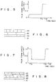
- Fig. 5 shows changes in Al film forming speed with respect to time when the Al film is formed on the substrate by depositing Al alloy by sputtering.
- the film forming speed is changed at two stages in such a way that the speed is 0.25 ( ⁇ m/min) from the start to the time point T21 and then 1.0 ( ⁇ m/min) from the time point T21 to T22.
- the heating temperature of the semiconductor substrate is 500°C and the Al film thickness is 5000 ⁇ at each stage.
- the target material is an Al alloy including 1% silicon.
- Fig. 6 shows a longitudinal cross section of the Al wiring layer of two divided sublayer structure formed in accordance with the method as described above.
- the heating temperature of the semiconductor substrate 31 is kept constant at 500°C, since the film forming speed is changed at two stages, the crystal grain sizes are different from each other between the two divided Al wiring sublayers 33 and 34 formed on the silicon oxide film 32.
- the deposited Al alloy is diffused and moved on the surface thereof on the basis of the phenomenon referred to as surface migration.
- the film forming speed is slow, since the speed at which the Al alloy is deposited is slow, the Al alloy deposited on the surface is easy to migrate and therefore the migration distant is large so that the crystal grain size is large.
- the film forming speed is high, since the deposition speed is high, the Al alloy deposited on the surface is difficult to migrate, so that the crystal grain size is small.
- the film forming speed at which the first divided Al wiring sublayer 33 is formed is slow as 0.25 ( ⁇ m/min) and the speed at which the second divided Al wiring sublayer 34 is high as 1.0 ( ⁇ m/min). Accordingly, the crystal grain size of the first divided Al wiring sublayer 33 is larger than that of the second divided Al wiring sublayer 34.
- Fig. 7 shows the third embodiment of the present invention, in which the film forming speed is changed at three stages.
- the film forming speed is determined as 1.0 ( ⁇ m/min) from the start to the time point T31, 0.25 ( ⁇ m/min) from the time point T31 to T32, and 1.0 ( ⁇ m/min) from the time point T32 to T33.
- the heating temperature of the semiconductor substrate is 500°C in the same way as with the case of the second embodiment, and the material is an Al alloy including 1% silicon.
- the film thickness is 3333 ⁇ at the respective stages.
- Fig. 8 shows a longitudinal cross section of the Al wiring layer formed by changing the film forming speed at three stages in accordance with the third embodiment, in which first, second and third divided Al wiring sublayers 43, 44 and 45 are formed on a silicon oxide film 42 of a semiconductor substrate 41.
- the crystal grain size is small in the first and third divided Al wiring sublayers 43 and 45 because the film forming speed is high, but the crystal grain size is large in the second divided Al wiring sublayer 44 because the speed is low.
- two or three divided Al wiring sublayers of different crystal grain sizes can be laminated. Therefore, the interfaces between adjoining crystal grain boundaries are offset from each other without being arranged in the film thickness direction in the same way as the first embodiment, thus improving the electromigration and stress migration resistances.
- the crystal grain size can be controlled into any desired value by changing the film forming speed, it is possible to obtain the Al wiring layer excellent in reproducibility and uniform in quality.
- the film thickness of the divided Al wiring sublayer is controllable precisely to any desired value by controlling the thickness of the Al or Al alloy deposited by sputtering.
- the manufacturing step of the second and third embodiments can be simplified in the same way as in the first embodiment.
- the semiconductor substrate is carried into the Al film forming equipment (in step 21); the Al film forming equipment is evacuated into a vacuum (in step 22); the divided Al wiring sublayers are laminated on the semiconductor substrate within the Al film forming equipment by stepwise changing the film forming speed (in step 23); the film forming equipment is deevacuated after the Al wiring layer has been formed (in step 24); and the semiconductor substrate is carried out (in step 25).
- the Al film forming equipment is evacuated and deevacuated one time each, respectively, it is possible to improve the productivity.
- the test results of the Al wiring layers formed in accordance with the second and third embodiments will be described hereinbelow with respect to the electromigration resistance.
- a silicon oxide film was formed on a semiconductor substrate, and an Al wiring layer of two- or three-sublayer structure was formed on the silicon oxide film in accordance with the film forming speed of the second or third embodiment.
- the formed wiring layer was patterned by photoetching method or RIE technique to obtain a 2 ⁇ m-wide and 1 ⁇ m-long straight wire.
- the test temperature was 200°C and the current density was 2.0 X 10⁶ A/cm2 in the same way as the test of the first embodiment.
- Fig. 9 shows the MTF values obtained as the test results, in which a solid line a indicates the MTF values of the Al wiring layers formed by the prior-art method (the same as shown in Fig. 4); a solid line c indicates the values of those formed by the second embodiment; and a solid line d indicates the values of those formed by the third embodiment.
- the MTF values of the Al wiring layers formed by the prior art range from about 800 to 4000 hours, so that the electromigration resistance is low.
- the MTF values of the Al wiring layers formed by the second embodiment concentrate from about 4000 to 5000 hours
- the values of those formed by the third embodiment concentrate from about 4500 to 5500 hours. This indicates that it is possible to form Al wiring layers excellent in electromigration resistance and with good reproducibility when the Al wiring layers are manufactured by changing the film forming speed at two or more stages as in the second or third embodiment.
- the semiconductor substrates were kept heated at a constant temperature of 500°C when the Al wiring layers were being formed.
- the tests were made to check the influence of the substrate heating temperature upon the MTF values.
- Fig. 10 shows the relationship between the substrate heating temperature and the MTF.
- the Al wiring layers were formed by setting the substrate heating temperature at six different values of 200°C (solid line e1); 300°C (e2); 400°C (e3); 420°C (e4); 440°C (e5); and 500°C (e6).
- Fig. 10 indicates that the MTF values of the Al wiring layers can be improved markedly when the substrate is heated at 440°C or higher.
- the substrate heating temperature is set at 440°C or higher and the film forming speed is changed at two or more stages when the Al wiring layers are formed in accordance with the second and third embodiments.
- the second and third embodiments are not limited to only the above description.
- the film forming speed can be changed at at least two stages, and therefore can be changed at four or more stages.
- a fourth embodiment of the present invention will be described hereinbelow.
- This fourth embodiment is characterized in that when the Al wiring layer is formed on the semiconductor substrate formed with a contact hole or a via hole, the semiconductor substrate is heated at 180°C or lower at the initial stage during which the hole is being buried by Al or Al alloy.
- An about 1 ⁇ m-thick silicon oxide film was formed on a semiconductor substrate and about 1 ⁇ m-dia. and 1 ⁇ m-deep holes were formed therein by photoetching method and RIE technique.
- a base film was formed by first forming a 300 ⁇ -thick Ti film on the silicon oxide film and inside the holes by sputtering, and further laminating a 1000 ⁇ -thick TiN film thereon by sputtering.
- test samples as described above were prepared, and a 0.2 ⁇ m thick Al wiring layer was formed thereon, respectively by changing the substrate heating temperature.
- the film thickness of 0.2 ⁇ m was measured at the flat areas (not within the hole) and the film forming speed was determined at 0.3 ( ⁇ m/min).
- the void occurrence status was observed by means of a scanning electron microscope by checking the hole side surfaces in the Al wiring layer.
- Figs. 11(a) to (d) show the inside states of the holes 57 obtained when the substrate heating temperature is set at 150, 180, 210, and 240°C, respectively.
- a 1 ⁇ m-thick silicon film 51 is formed on the semiconductor substrate 50; a 1 ⁇ m-dia. and 1 ⁇ m-deep hole 57 is formed in the silicon oxide film 51; and a base film 52 composed of Ti and TiN films are formed thereon.
- the Al wiring layer is formed so as to bury the hole, it is possible to form the Al film uniformly on the hole side surfaces by heating the substrate at 180°C or low at the initial stage.
- the time duration of the initial stage differs according to the diameter and depth of the hole. However, it is possible to determine the initial stage until the thickness of the Al film at the flat portions reaches about 1000 ⁇ .
- the inside statues of the holes were checked by forming an about 0.2 ⁇ m-thick Al wiring layer at different substrate heating temperatures at the initial stage and further forming an about 0.8 ⁇ m-thick Al wiring layer thereon by increasing the heating temperature up to 460°C.
- Fig. 12(a) no void was produced in the hole when the substrate was heated at 150°C at the initial stage.
- no void was produced when heated at 180°C at the initial stage as shown in Fig. 12(b).
- a void 64 was produced inside the hole 57 of the Al wiring layer 63 when the substrate was heated at 210°C.
- the substrate heating temperature is set as described above, it is possible to improve the electromigration and stress migration resistances at the areas other than the holes, as described in the second and third embodiments.
- a fifth embodiment of the present invention will be described hereinbelow. Similarly to the fourth embodiment, this embodiment relates to the method of forming an Al wiring layer on a semiconductor substrate formed with holes.
- This fifth embodiment is characterized in that the film forming speed is reduced intentionally at the initial stage during which the hole is being buried by Al or Al alloy.
- the film forming speed can be reduced by decreasing the speed and density of ions collided against the Al target in Ar gas, for instance.
- Fig. 13(a) is a plan view showing evaluating base layers
- Fig. 13(b) is a cross-sectional view taken along the line A-A shown in Fig. 13(a).
- the evaluating base layers were formed in such a way that: an about 1000 ⁇ thick thermal oxide film 105 was formed on a semiconductor substrate 100; a 5000 ⁇ -thick Al film was formed on the oxide film 105; the Al film was patterned by photoetching method to form 100-piece Al wiring layers 101 with a width of 1.5 ⁇ m and a length of 1 mm at intervals of 4 ⁇ m so that each Al wiring layer was formed with a 100 ⁇ m-square pad 101a on both the ends thereof, respectively; a 1.0 ⁇ m thick silicon oxide film 103 was deposited on the Al wiring layers 101 by CVD method; and finally a 1.0 ⁇ m dia. through holes 102 were opened over the lower Al wiring layers 101 by RIE method.
- an Al film with a thickness of 1.0 ⁇ m was formed by sputtering, respectively in accordance with the prior art method and the fifth embodiment method.
- the film forming speed was fixed at 1.0 ⁇ m/min.
- the film forming speed was determined at 0.1 ⁇ m/min at the initial stage and at 1.0 ⁇ m/min thereafter.
- Al alloy including 1% silicon was used.
- Al wiring layers with a width of 0.8 ⁇ m and a length of 1 mm, respectively were formed by RIE method.
- Fig. 14(a) is a plane view showing the obtained Al wiring layer and Fig.
- each upper Al wiring layer 104 is formed with a 100 ⁇ m square pad 104a on both ends thereof, respectively.
- the film forming speed was determined at 0.1 ⁇ m/min at the initial stage and at 1.0 ⁇ m/min thereafter. Without being limited thereto, it is also possible to change the film forming speed according to the aspect ratio of the hole. At the initial stage, in particular, the film forming speed is determined slow to such an extent that Al or Al alloy can smoothly bury the holes without being bridged over the holes.
Landscapes
- Internal Circuitry In Semiconductor Integrated Circuit Devices (AREA)
- Electrodes Of Semiconductors (AREA)
Applications Claiming Priority (4)
| Application Number | Priority Date | Filing Date | Title |
|---|---|---|---|
| JP336062/90 | 1990-11-30 | ||
| JP33606290 | 1990-11-30 | ||
| JP3296035A JPH04363024A (ja) | 1990-11-30 | 1991-11-12 | 半導体装置の製造方法 |
| JP296035/91 | 1991-11-12 |
Publications (2)
| Publication Number | Publication Date |
|---|---|
| EP0488264A2 true EP0488264A2 (de) | 1992-06-03 |
| EP0488264A3 EP0488264A3 (en) | 1992-07-22 |
Family
ID=26560516
Family Applications (1)
| Application Number | Title | Priority Date | Filing Date |
|---|---|---|---|
| EP19910120354 Ceased EP0488264A3 (en) | 1990-11-30 | 1991-11-28 | Method of manufacturing a semiconductor device with improved electromigration resistance |
Country Status (4)
| Country | Link |
|---|---|
| US (1) | US5407863A (de) |
| EP (1) | EP0488264A3 (de) |
| JP (1) | JPH04363024A (de) |
| KR (1) | KR950014267B1 (de) |
Cited By (16)
| Publication number | Priority date | Publication date | Assignee | Title |
|---|---|---|---|---|
| EP0586803A1 (de) * | 1992-08-12 | 1994-03-16 | Applied Materials, Inc. | Verfahren zur Herstellung von Via-Verbindungen mit geringem Widerstand aus Aluminium, verbunden mit einer darüberliegenden Schaltungsschicht aus Metall für integrierte Schaltungsstruktur |
| EP0594300A1 (de) * | 1992-09-22 | 1994-04-27 | STMicroelectronics, Inc. | Methode zur Herstellung eines Metallkontaktes |
| US5472912A (en) * | 1989-11-30 | 1995-12-05 | Sgs-Thomson Microelectronics, Inc. | Method of making an integrated circuit structure by using a non-conductive plug |
| EP0716447A3 (de) * | 1994-12-05 | 1997-01-08 | At & T Corp | Aus geschichteten Subschichten geformte Metallschichten und Anordnungen mit diesen Metallschichten |
| EP0720211A3 (de) * | 1994-12-30 | 1997-03-05 | At & T Corp | Verfahren zur Abscheidung von Wolfram |
| US5658828A (en) * | 1989-11-30 | 1997-08-19 | Sgs-Thomson Microelectronics, Inc. | Method for forming an aluminum contact through an insulating layer |
| EP0706205A3 (de) * | 1994-09-19 | 1997-10-22 | Siemens Ag | Verfahren zur planarisierenden Sputterabscheidung einer aluminiumhaltigen Schicht bei der Herstellung integrierter Schaltungen |
| US5723367A (en) * | 1993-11-16 | 1998-03-03 | Kabushiki Kaisha Toshiba | Wiring forming method |
| GB2323475A (en) * | 1995-11-21 | 1998-09-23 | Lg Electronics Inc | Controlling the generation of hillocks in liquid crystal devices |
| US5930673A (en) * | 1990-11-05 | 1999-07-27 | Stmicroelectronics, Inc. | Method for forming a metal contact |
| GB2307597B (en) * | 1995-11-21 | 1999-08-11 | Lg Electronics Inc | Controlling the generating of hillocks in liquid crystal devices |
| EP0856885A3 (de) * | 1997-02-03 | 2000-05-31 | Applied Materials, Inc. | Verfahren und Vorrichtung zur Reduzierung des "Erste-Scheibe-Effekts" |
| US6242811B1 (en) | 1989-11-30 | 2001-06-05 | Stmicroelectronics, Inc. | Interlevel contact including aluminum-refractory metal alloy formed during aluminum deposition at an elevated temperature |
| US6271137B1 (en) | 1989-11-30 | 2001-08-07 | Stmicroelectronics, Inc. | Method of producing an aluminum stacked contact/via for multilayer |
| US6287963B1 (en) | 1990-11-05 | 2001-09-11 | Stmicroelectronics, Inc. | Method for forming a metal contact |
| US6617242B1 (en) | 1989-11-30 | 2003-09-09 | Stmicroelectronics, Inc. | Method for fabricating interlevel contacts of aluminum/refractory metal alloys |
Families Citing this family (23)
| Publication number | Priority date | Publication date | Assignee | Title |
|---|---|---|---|---|
| US5747360A (en) * | 1993-09-17 | 1998-05-05 | Applied Materials, Inc. | Method of metalizing a semiconductor wafer |
| US5561083A (en) * | 1994-12-29 | 1996-10-01 | Lucent Technologies Inc. | Method of making multilayered Al-alloy structure for metal conductors |
| US6285082B1 (en) * | 1995-01-03 | 2001-09-04 | International Business Machines Corporation | Soft metal conductor |
| JPH08191104A (ja) | 1995-01-11 | 1996-07-23 | Hitachi Ltd | 半導体集積回路装置およびその製造方法 |
| US5494860A (en) * | 1995-03-14 | 1996-02-27 | International Business Machines Corporation | Two step annealing process for decreasing contact resistance |
| KR0179827B1 (ko) * | 1995-05-27 | 1999-04-15 | 문정환 | 반도체 소자의 배선 형성방법 |
| WO1996039714A1 (en) * | 1995-06-06 | 1996-12-12 | International Business Machines Corporation | Method for reducing a transient thermal mismatch |
| US5851920A (en) * | 1996-01-22 | 1998-12-22 | Motorola, Inc. | Method of fabrication of metallization system |
| US6291336B1 (en) | 1996-05-20 | 2001-09-18 | Taiwan Semiconductor Manufacturing Company | AlCu metal deposition for robust Rc via performance |
| US6083823A (en) * | 1996-06-28 | 2000-07-04 | International Business Machines Corporation | Metal deposition process for metal lines over topography |
| US5930587A (en) * | 1997-08-27 | 1999-07-27 | Lucent Technologies | Stress migration evaluation method |
| JP2000150653A (ja) * | 1998-09-04 | 2000-05-30 | Seiko Epson Corp | 半導体装置の製造方法 |
| JP3533968B2 (ja) | 1998-12-22 | 2004-06-07 | セイコーエプソン株式会社 | 半導体装置の製造方法 |
| US6136709A (en) * | 1999-10-06 | 2000-10-24 | Infineon Technologies North America Corp. | Metal line deposition process |
| US6943105B2 (en) | 2002-01-18 | 2005-09-13 | International Business Machines Corporation | Soft metal conductor and method of making |
| US6919568B2 (en) * | 2003-04-08 | 2005-07-19 | Ge Medical Systems Global Technology Company Llc | Method and apparatus for identifying composite defective pixel map |
| US20060180934A1 (en) * | 2005-02-14 | 2006-08-17 | Taiwan Semiconductor Manufacturing Co., Ltd. | Wiring structures for semiconductor devices |
| JP5181462B2 (ja) * | 2006-10-31 | 2013-04-10 | 富士ゼロックス株式会社 | 半導体素子及びその製造方法 |
| JP5352954B2 (ja) * | 2006-11-22 | 2013-11-27 | 日産自動車株式会社 | 電極膜/炭化珪素構造体 |
| JP6341126B2 (ja) * | 2015-03-20 | 2018-06-13 | 豊田合成株式会社 | 半導体装置および半導体装置の製造方法 |
| US11670485B2 (en) * | 2019-08-20 | 2023-06-06 | Applied Materials, Inc. | Methods and apparatus for depositing aluminum by physical vapor deposition (PVD) |
| US11315771B2 (en) * | 2020-07-14 | 2022-04-26 | Applied Materials, Inc. | Methods and apparatus for processing a substrate |
| US20250242406A1 (en) * | 2024-01-25 | 2025-07-31 | Applied Materials, Inc. | Alloy microstructure formation for chamber components |
Family Cites Families (14)
| Publication number | Priority date | Publication date | Assignee | Title |
|---|---|---|---|---|
| US4495221A (en) * | 1982-10-26 | 1985-01-22 | Signetics Corporation | Variable rate semiconductor deposition process |
| US4566177A (en) * | 1984-05-11 | 1986-01-28 | Signetics Corporation | Formation of electromigration resistant aluminum alloy conductors |
| US4796562A (en) * | 1985-12-03 | 1989-01-10 | Varian Associates, Inc. | Rapid thermal cvd apparatus |
| JPS6474739A (en) * | 1987-09-17 | 1989-03-20 | Fujitsu Ltd | Manufacture of semiconductor device |
| JPH01150335A (ja) * | 1987-12-07 | 1989-06-13 | Nec Corp | アルミニウム系薄膜配線 |
| JPH01160036A (ja) * | 1987-12-17 | 1989-06-22 | Oki Electric Ind Co Ltd | 半導体装置 |
| JPH01191442A (ja) * | 1988-01-27 | 1989-08-01 | Nec Corp | 半導体集積回路装置の製造方法 |
| JPH01261846A (ja) * | 1988-04-13 | 1989-10-18 | Hitachi Ltd | 半導体素子およびその製造方法 |
| US4837183A (en) * | 1988-05-02 | 1989-06-06 | Motorola Inc. | Semiconductor device metallization process |
| FR2634317A1 (fr) * | 1988-07-12 | 1990-01-19 | Philips Nv | Procede pour fabriquer un dispositif semiconducteur ayant au moins un niveau de prise de contact a travers des ouvertures de contact de petites dimensions |
| JPH02178923A (ja) * | 1988-12-29 | 1990-07-11 | Fujitsu Ltd | 半導体装置の製造方法 |
| US4970176A (en) * | 1989-09-29 | 1990-11-13 | Motorola, Inc. | Multiple step metallization process |
| US5108951A (en) * | 1990-11-05 | 1992-04-28 | Sgs-Thomson Microelectronics, Inc. | Method for forming a metal contact |
| US5108570A (en) * | 1990-03-30 | 1992-04-28 | Applied Materials, Inc. | Multistep sputtering process for forming aluminum layer over stepped semiconductor wafer |
-
1991
- 1991-11-12 JP JP3296035A patent/JPH04363024A/ja active Pending
- 1991-11-28 KR KR1019910021468A patent/KR950014267B1/ko not_active Expired - Lifetime
- 1991-11-28 EP EP19910120354 patent/EP0488264A3/en not_active Ceased
- 1991-11-29 US US07/798,706 patent/US5407863A/en not_active Expired - Lifetime
Cited By (20)
| Publication number | Priority date | Publication date | Assignee | Title |
|---|---|---|---|---|
| US6242811B1 (en) | 1989-11-30 | 2001-06-05 | Stmicroelectronics, Inc. | Interlevel contact including aluminum-refractory metal alloy formed during aluminum deposition at an elevated temperature |
| US5976969A (en) * | 1989-11-30 | 1999-11-02 | Stmicroelectronics, Inc. | Method for forming an aluminum contact |
| US5472912A (en) * | 1989-11-30 | 1995-12-05 | Sgs-Thomson Microelectronics, Inc. | Method of making an integrated circuit structure by using a non-conductive plug |
| US6617242B1 (en) | 1989-11-30 | 2003-09-09 | Stmicroelectronics, Inc. | Method for fabricating interlevel contacts of aluminum/refractory metal alloys |
| US5658828A (en) * | 1989-11-30 | 1997-08-19 | Sgs-Thomson Microelectronics, Inc. | Method for forming an aluminum contact through an insulating layer |
| US6271137B1 (en) | 1989-11-30 | 2001-08-07 | Stmicroelectronics, Inc. | Method of producing an aluminum stacked contact/via for multilayer |
| US6287963B1 (en) | 1990-11-05 | 2001-09-11 | Stmicroelectronics, Inc. | Method for forming a metal contact |
| US5930673A (en) * | 1990-11-05 | 1999-07-27 | Stmicroelectronics, Inc. | Method for forming a metal contact |
| EP0586803A1 (de) * | 1992-08-12 | 1994-03-16 | Applied Materials, Inc. | Verfahren zur Herstellung von Via-Verbindungen mit geringem Widerstand aus Aluminium, verbunden mit einer darüberliegenden Schaltungsschicht aus Metall für integrierte Schaltungsstruktur |
| EP0594300A1 (de) * | 1992-09-22 | 1994-04-27 | STMicroelectronics, Inc. | Methode zur Herstellung eines Metallkontaktes |
| US5723367A (en) * | 1993-11-16 | 1998-03-03 | Kabushiki Kaisha Toshiba | Wiring forming method |
| US6433435B2 (en) | 1993-11-30 | 2002-08-13 | Stmicroelectronics, Inc. | Aluminum contact structure for integrated circuits |
| EP0706205A3 (de) * | 1994-09-19 | 1997-10-22 | Siemens Ag | Verfahren zur planarisierenden Sputterabscheidung einer aluminiumhaltigen Schicht bei der Herstellung integrierter Schaltungen |
| EP0716447A3 (de) * | 1994-12-05 | 1997-01-08 | At & T Corp | Aus geschichteten Subschichten geformte Metallschichten und Anordnungen mit diesen Metallschichten |
| EP0720211A3 (de) * | 1994-12-30 | 1997-03-05 | At & T Corp | Verfahren zur Abscheidung von Wolfram |
| GB2323475A (en) * | 1995-11-21 | 1998-09-23 | Lg Electronics Inc | Controlling the generation of hillocks in liquid crystal devices |
| GB2307597B (en) * | 1995-11-21 | 1999-08-11 | Lg Electronics Inc | Controlling the generating of hillocks in liquid crystal devices |
| GB2323475B (en) * | 1995-11-21 | 1999-08-11 | Lg Electronics Inc | Controlling the generation of hillocks in liquid crystal devices |
| EP0856885A3 (de) * | 1997-02-03 | 2000-05-31 | Applied Materials, Inc. | Verfahren und Vorrichtung zur Reduzierung des "Erste-Scheibe-Effekts" |
| US6139698A (en) * | 1997-02-03 | 2000-10-31 | Applied Materials, Inc. | Method and apparatus for reducing the first wafer effect |
Also Published As
| Publication number | Publication date |
|---|---|
| JPH04363024A (ja) | 1992-12-15 |
| US5407863A (en) | 1995-04-18 |
| KR950014267B1 (ko) | 1995-11-24 |
| EP0488264A3 (en) | 1992-07-22 |
Similar Documents
| Publication | Publication Date | Title |
|---|---|---|
| US5407863A (en) | Method of manufacturing semiconductor device | |
| US5766379A (en) | Passivated copper conductive layers for microelectronic applications and methods of manufacturing same | |
| JP5132400B2 (ja) | 軟金属導体およびその形成方法 | |
| US4937652A (en) | Semiconductor device and method of manufacturing the same | |
| US5412160A (en) | Circuit board | |
| EP0526889B1 (de) | Verfahren zum Aufbringen einer Metall- oder Passivierenschicht mit hoher Haftung über einem isolierten Halbleitersubstrat | |
| CA1276088C (en) | Enhanced adhesion between metals and polymers | |
| CN1115718C (zh) | 形成半导体装置的金属接线的方法 | |
| KR100451279B1 (ko) | 구리 배선 | |
| EP0840370B1 (de) | Niedrigtemperatur-Aluminiumaufschmelzen für mehrschichtige Metallisierung | |
| WO1993013555A1 (fr) | Dispositif a semi-conducteurs | |
| US5200030A (en) | Method for manufacturing a planarized metal layer for semiconductor device | |
| WO1987002828A1 (en) | Glass intermetal dielectric | |
| KR100213447B1 (ko) | 반도체 소자의 금속 배선 형성방법 | |
| CN1198252A (zh) | 用于集成电路的含有用专用腔室淀积的两薄层钛的金属堆栈 | |
| JP2004140198A (ja) | 半導体装置およびその製造方法 | |
| US6004827A (en) | Integrated circuit processing | |
| JPS60262443A (ja) | 多層配線の形成方法 | |
| JPH06140401A (ja) | 集積回路装置 | |
| US4992152A (en) | Reducing hillocking in aluminum layers formed on substrates | |
| JP2004274065A (ja) | ボイドのないビアの形成法 | |
| KR100297354B1 (ko) | 스퍼터링법에 의한 다층 구리막 제조방법 | |
| JPH04116829A (ja) | 半導体装置およびその製造方法 | |
| KR100199910B1 (ko) | 반도체 소자 제조 방법 | |
| US5989442A (en) | Wet etching |
Legal Events
| Date | Code | Title | Description |
|---|---|---|---|
| PUAI | Public reference made under article 153(3) epc to a published international application that has entered the european phase |
Free format text: ORIGINAL CODE: 0009012 |
|
| PUAL | Search report despatched |
Free format text: ORIGINAL CODE: 0009013 |
|
| 17P | Request for examination filed |
Effective date: 19911128 |
|
| AK | Designated contracting states |
Kind code of ref document: A2 Designated state(s): DE FR GB |
|
| AK | Designated contracting states |
Kind code of ref document: A3 Designated state(s): DE FR GB |
|
| 17Q | First examination report despatched |
Effective date: 19941206 |
|
| APAB | Appeal dossier modified |
Free format text: ORIGINAL CODE: EPIDOS NOAPE |
|
| APAB | Appeal dossier modified |
Free format text: ORIGINAL CODE: EPIDOS NOAPE |
|
| APAD | Appeal reference recorded |
Free format text: ORIGINAL CODE: EPIDOS REFNE |
|
| APAD | Appeal reference recorded |
Free format text: ORIGINAL CODE: EPIDOS REFNE |
|
| STAA | Information on the status of an ep patent application or granted ep patent |
Free format text: STATUS: THE APPLICATION HAS BEEN REFUSED |
|
| 18R | Application refused |
Effective date: 20021007 |
|
| APAF | Appeal reference modified |
Free format text: ORIGINAL CODE: EPIDOSCREFNE |