US4992152A - Reducing hillocking in aluminum layers formed on substrates - Google Patents
Reducing hillocking in aluminum layers formed on substrates Download PDFInfo
- Publication number
- US4992152A US4992152A US07/504,362 US50436290A US4992152A US 4992152 A US4992152 A US 4992152A US 50436290 A US50436290 A US 50436290A US 4992152 A US4992152 A US 4992152A
- Authority
- US
- United States
- Prior art keywords
- layer
- aluminum
- substrate
- layers
- reducing
- Prior art date
- Legal status (The legal status is an assumption and is not a legal conclusion. Google has not performed a legal analysis and makes no representation as to the accuracy of the status listed.)
- Expired - Fee Related
Links
Images

Classifications
-
- C—CHEMISTRY; METALLURGY
- C23—COATING METALLIC MATERIAL; COATING MATERIAL WITH METALLIC MATERIAL; CHEMICAL SURFACE TREATMENT; DIFFUSION TREATMENT OF METALLIC MATERIAL; COATING BY VACUUM EVAPORATION, BY SPUTTERING, BY ION IMPLANTATION OR BY CHEMICAL VAPOUR DEPOSITION, IN GENERAL; INHIBITING CORROSION OF METALLIC MATERIAL OR INCRUSTATION IN GENERAL
- C23C—COATING METALLIC MATERIAL; COATING MATERIAL WITH METALLIC MATERIAL; SURFACE TREATMENT OF METALLIC MATERIAL BY DIFFUSION INTO THE SURFACE, BY CHEMICAL CONVERSION OR SUBSTITUTION; COATING BY VACUUM EVAPORATION, BY SPUTTERING, BY ION IMPLANTATION OR BY CHEMICAL VAPOUR DEPOSITION, IN GENERAL
- C23C14/00—Coating by vacuum evaporation, by sputtering or by ion implantation of the coating forming material
- C23C14/58—After-treatment
- C23C14/5806—Thermal treatment
-
- C—CHEMISTRY; METALLURGY
- C23—COATING METALLIC MATERIAL; COATING MATERIAL WITH METALLIC MATERIAL; CHEMICAL SURFACE TREATMENT; DIFFUSION TREATMENT OF METALLIC MATERIAL; COATING BY VACUUM EVAPORATION, BY SPUTTERING, BY ION IMPLANTATION OR BY CHEMICAL VAPOUR DEPOSITION, IN GENERAL; INHIBITING CORROSION OF METALLIC MATERIAL OR INCRUSTATION IN GENERAL
- C23C—COATING METALLIC MATERIAL; COATING MATERIAL WITH METALLIC MATERIAL; SURFACE TREATMENT OF METALLIC MATERIAL BY DIFFUSION INTO THE SURFACE, BY CHEMICAL CONVERSION OR SUBSTITUTION; COATING BY VACUUM EVAPORATION, BY SPUTTERING, BY ION IMPLANTATION OR BY CHEMICAL VAPOUR DEPOSITION, IN GENERAL
- C23C14/00—Coating by vacuum evaporation, by sputtering or by ion implantation of the coating forming material
- C23C14/06—Coating by vacuum evaporation, by sputtering or by ion implantation of the coating forming material characterised by the coating material
- C23C14/0682—Silicides
-
- C—CHEMISTRY; METALLURGY
- C23—COATING METALLIC MATERIAL; COATING MATERIAL WITH METALLIC MATERIAL; CHEMICAL SURFACE TREATMENT; DIFFUSION TREATMENT OF METALLIC MATERIAL; COATING BY VACUUM EVAPORATION, BY SPUTTERING, BY ION IMPLANTATION OR BY CHEMICAL VAPOUR DEPOSITION, IN GENERAL; INHIBITING CORROSION OF METALLIC MATERIAL OR INCRUSTATION IN GENERAL
- C23C—COATING METALLIC MATERIAL; COATING MATERIAL WITH METALLIC MATERIAL; SURFACE TREATMENT OF METALLIC MATERIAL BY DIFFUSION INTO THE SURFACE, BY CHEMICAL CONVERSION OR SUBSTITUTION; COATING BY VACUUM EVAPORATION, BY SPUTTERING, BY ION IMPLANTATION OR BY CHEMICAL VAPOUR DEPOSITION, IN GENERAL
- C23C14/00—Coating by vacuum evaporation, by sputtering or by ion implantation of the coating forming material
- C23C14/06—Coating by vacuum evaporation, by sputtering or by ion implantation of the coating forming material characterised by the coating material
- C23C14/14—Metallic material, boron or silicon
- C23C14/16—Metallic material, boron or silicon on metallic substrates or on substrates of boron or silicon
-
- C—CHEMISTRY; METALLURGY
- C23—COATING METALLIC MATERIAL; COATING MATERIAL WITH METALLIC MATERIAL; CHEMICAL SURFACE TREATMENT; DIFFUSION TREATMENT OF METALLIC MATERIAL; COATING BY VACUUM EVAPORATION, BY SPUTTERING, BY ION IMPLANTATION OR BY CHEMICAL VAPOUR DEPOSITION, IN GENERAL; INHIBITING CORROSION OF METALLIC MATERIAL OR INCRUSTATION IN GENERAL
- C23C—COATING METALLIC MATERIAL; COATING MATERIAL WITH METALLIC MATERIAL; SURFACE TREATMENT OF METALLIC MATERIAL BY DIFFUSION INTO THE SURFACE, BY CHEMICAL CONVERSION OR SUBSTITUTION; COATING BY VACUUM EVAPORATION, BY SPUTTERING, BY ION IMPLANTATION OR BY CHEMICAL VAPOUR DEPOSITION, IN GENERAL
- C23C14/00—Coating by vacuum evaporation, by sputtering or by ion implantation of the coating forming material
- C23C14/58—After-treatment
-
- H—ELECTRICITY
- H01—ELECTRIC ELEMENTS
- H01L—SEMICONDUCTOR DEVICES NOT COVERED BY CLASS H10
- H01L21/00—Processes or apparatus adapted for the manufacture or treatment of semiconductor or solid state devices or of parts thereof
- H01L21/70—Manufacture or treatment of devices consisting of a plurality of solid state components formed in or on a common substrate or of parts thereof; Manufacture of integrated circuit devices or of parts thereof
- H01L21/71—Manufacture of specific parts of devices defined in group H01L21/70
- H01L21/768—Applying interconnections to be used for carrying current between separate components within a device comprising conductors and dielectrics
- H01L21/76838—Applying interconnections to be used for carrying current between separate components within a device comprising conductors and dielectrics characterised by the formation and the after-treatment of the conductors
- H01L21/76886—Modifying permanently or temporarily the pattern or the conductivity of conductive members, e.g. formation of alloys, reduction of contact resistances
-
- H—ELECTRICITY
- H01—ELECTRIC ELEMENTS
- H01L—SEMICONDUCTOR DEVICES NOT COVERED BY CLASS H10
- H01L23/00—Details of semiconductor or other solid state devices
- H01L23/52—Arrangements for conducting electric current within the device in operation from one component to another, i.e. interconnections, e.g. wires, lead frames
- H01L23/522—Arrangements for conducting electric current within the device in operation from one component to another, i.e. interconnections, e.g. wires, lead frames including external interconnections consisting of a multilayer structure of conductive and insulating layers inseparably formed on the semiconductor body
- H01L23/532—Arrangements for conducting electric current within the device in operation from one component to another, i.e. interconnections, e.g. wires, lead frames including external interconnections consisting of a multilayer structure of conductive and insulating layers inseparably formed on the semiconductor body characterised by the materials
- H01L23/53204—Conductive materials
- H01L23/53209—Conductive materials based on metals, e.g. alloys, metal silicides
- H01L23/53214—Conductive materials based on metals, e.g. alloys, metal silicides the principal metal being aluminium
- H01L23/53223—Additional layers associated with aluminium layers, e.g. adhesion, barrier, cladding layers
-
- H—ELECTRICITY
- H01—ELECTRIC ELEMENTS
- H01L—SEMICONDUCTOR DEVICES NOT COVERED BY CLASS H10
- H01L2924/00—Indexing scheme for arrangements or methods for connecting or disconnecting semiconductor or solid-state bodies as covered by H01L24/00
- H01L2924/0001—Technical content checked by a classifier
- H01L2924/0002—Not covered by any one of groups H01L24/00, H01L24/00 and H01L2224/00
-
- Y—GENERAL TAGGING OF NEW TECHNOLOGICAL DEVELOPMENTS; GENERAL TAGGING OF CROSS-SECTIONAL TECHNOLOGIES SPANNING OVER SEVERAL SECTIONS OF THE IPC; TECHNICAL SUBJECTS COVERED BY FORMER USPC CROSS-REFERENCE ART COLLECTIONS [XRACs] AND DIGESTS
- Y10—TECHNICAL SUBJECTS COVERED BY FORMER USPC
- Y10S—TECHNICAL SUBJECTS COVERED BY FORMER USPC CROSS-REFERENCE ART COLLECTIONS [XRACs] AND DIGESTS
- Y10S438/00—Semiconductor device manufacturing: process
- Y10S438/937—Hillock prevention
Definitions
- This invention relates to a method for reducing the formation of hillocks in aluminum layers sputtered onto substrates.
- a thin aluminum layer is deposited by sputtering onto a substrate. Atoms of aluminum from a target are ejected from the target by impact from an ionized gas. The aluminum atoms are then deposited on the surface of the substrate.
- these microscopic protrusions or hillocks are troublesome and can cause subsequent device failure.
- hillocks can cause shorts between conductive layers in a device in areas where conductors cross over one another, or in elements of the device having two layers of conductors such as integrated capacitors. More particularly, if an insulating layer, e.g. SiO 2 is formed on an aluminum layer at a thickness of less than 1 ⁇ metal hillocks greater than 1 ⁇ will protrude through the SiO 2 layer and contact any subsequently deposited metal layers, causing a short circuit.
- an insulating layer e.g. SiO 2
- the protrusion of the hillocks potentially causes short circuits between conductive layers in a device at positions where the conductors cross over each other, or in devices where there are two spaced apart layers such as in capacitors, forming part of an integrated circuit.
- Hillocks are also found in aluminum layers formed in optical disks.
- SiO 2 is frequently deposited on the metal layer and then in particular locations etched down to the surface of the metal by HF acid.
- HF also attacks tantalum silicide and at an etch rate of 300-600 ⁇ /min.
- the object of this invention is to provide a simple, effective means of reducing hillock formation in aluminum layers sputtered onto a substrate eliminating the problems discussed above.
- This object is achieved in a method in which aluminum is sputtered from a target onto the surface of a substrate to deposit a layer of aluminum metal.
- a layer of WSi 2 is deposited on the aluminum layer in the same vacuum and both layers are then sintered, so when sintered these layers react and reduce hillock formation.
- a feature of this invention is that WSi 2 in not subject to attack by HF.
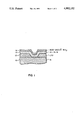
- FIG. 1 shows the final structure produced by the process of this invention
- FIG. 3 is a graph of the surface roughness of 8000 ⁇ layer of aluminum coated on a substrate; after three sinters. Each sinter is at 450° C. for 30 minutes: and
- FIG. 2 is a graph of the surface roughness of an 8000 ⁇ layer of aluminum coated on a substrate and a 2000 ⁇ layer of WSi 2 coated on the aluminum layer in the same vacuum after three sinters.
- the term "substrate” means the underlying material such as for example silicon, silicon dioxide or silicon nitride on which an aluminum layer is deposited.
- the term “substrate” does not, however, mean only the base material forming the wafer on which a device such as an integrated circuit is fabricated.
- the substrate on which the aluminum layer is applied may also include appropriate dopants to provide n or p type dopings depending upon the device being fabricated. It is preferable that the deposited aluminum layer has a significantly higher coefficient of thermal expansion than the selected substrate.
- ordinarily aluminum targets are doped with 1% silicon and sometimes from 1 to 4% copper. These impurities help to prevent cracks from forming at the interface between the deposited aluminum layer and the substrate.
- a Si substrate is indicated as layer 10.
- a dielectric layer 12 such as low temperature oxide (LTO).
- LTO low temperature oxide
- the purpose of layer 12 is to isolate the metal layers from the underlying substrate in all regions except where contact is desired. Openings are formed in layer 12 exposing the Si substrate by means of lithography and etching.
- a layer 14 of WSi 2 which has a thickness between 1500-2500 ⁇ , is sputtered onto layer 13.
- Layer 13 may be in a range in thickness between 6000 and 9000 ⁇ .
- layer 14 be sputtered directly on layer 13 without breaking the vacuum in the sputter chamber, as this does not permit the formation of a native oxide on the Al layer.
- Subsequent sintering of this structure permits reaction between the WSi 2 layer 13 and all of layer 14 that eliminates hillock formation.
- the length of sintering that is adequate ranges from 30 minutes at 450° C. to 120 minutes at 450° C. in a forming gas ambient.
- a number of different devices have been made using this process. In such devices, hillock formation has been substantially reduced.
- the former conditions are typical of those used in post metallization anneals, while the latter condition includes adequate thermal budget to simulate any intermediate dielectric depositions that may be required.
- FIG. 3 we see a graph of the surface roughness of a layer of 8000 ⁇ aluminum coated on a Si substrate. This structure was sintered three times. For each sinter, the wafers were heater to 450° C. in a forming gas ambient and kept there for 30 minutes. The wafers were cooled to room temperature between sinters.
- the horizontal axis is labeled "Distance along the surface ( ⁇ m)." It represents the distance over which a stylus was dragged along the surface. The axis is measured in microns.
- the vertical axis is the vertical dimension of the surface roughness. The maximum range shown in the figure is 5000 ⁇ . This graph shows that the surface is quite rough and can produce hillocks as large as 4000 ⁇ .
- FIG. 2 a 2000 ⁇ layer of WSi 2 coated on an 8000 ⁇ layer of aluminum was sintered three times. The same vertical and horizontal axes as FIG. 2 were used. The resulting surface was quite smooth.
- a feature of WSi 2 is that it is not subject to attack by HF.
Abstract
Description
Claims (1)
Priority Applications (1)
| Application Number | Priority Date | Filing Date | Title |
|---|---|---|---|
| US07/504,362 US4992152A (en) | 1989-04-20 | 1990-04-04 | Reducing hillocking in aluminum layers formed on substrates |
Applications Claiming Priority (2)
| Application Number | Priority Date | Filing Date | Title |
|---|---|---|---|
| US34126689A | 1989-04-20 | 1989-04-20 | |
| US07/504,362 US4992152A (en) | 1989-04-20 | 1990-04-04 | Reducing hillocking in aluminum layers formed on substrates |
Related Parent Applications (1)
| Application Number | Title | Priority Date | Filing Date |
|---|---|---|---|
| US34126689A Continuation-In-Part | 1989-04-20 | 1989-04-20 |
Publications (1)
| Publication Number | Publication Date |
|---|---|
| US4992152A true US4992152A (en) | 1991-02-12 |
Family
ID=26992436
Family Applications (1)
| Application Number | Title | Priority Date | Filing Date |
|---|---|---|---|
| US07/504,362 Expired - Fee Related US4992152A (en) | 1989-04-20 | 1990-04-04 | Reducing hillocking in aluminum layers formed on substrates |
Country Status (1)
| Country | Link |
|---|---|
| US (1) | US4992152A (en) |
Cited By (3)
| Publication number | Priority date | Publication date | Assignee | Title |
|---|---|---|---|---|
| US5629218A (en) * | 1989-12-19 | 1997-05-13 | Texas Instruments Incorporated | Method for forming a field-effect transistor including a mask body and source/drain contacts |
| US5843842A (en) * | 1991-07-08 | 1998-12-01 | Samsung Electronics Co., Ltd. | Method for manufacturing a semiconductor device having a wiring layer without producing silicon precipitates |
| US8822336B2 (en) | 2011-06-16 | 2014-09-02 | United Microelectronics Corp. | Through-silicon via forming method |
Citations (9)
| Publication number | Priority date | Publication date | Assignee | Title |
|---|---|---|---|---|
| US3986897A (en) * | 1974-09-30 | 1976-10-19 | Motorola, Inc. | Aluminum treatment to prevent hillocking |
| US4012756A (en) * | 1969-12-30 | 1977-03-15 | International Business Machines Corporation | Method of inhibiting hillock formation in films and film thereby and multilayer structure therewith |
| JPS5737856A (en) * | 1980-08-20 | 1982-03-02 | Fujitsu Ltd | Semiconductor device |
| US4322453A (en) * | 1980-12-08 | 1982-03-30 | International Business Machines Corporation | Conductivity WSi2 (tungsten silicide) films by Pt preanneal layering |
| US4384301A (en) * | 1979-11-07 | 1983-05-17 | Texas Instruments Incorporated | High performance submicron metal-oxide-semiconductor field effect transistor device structure |
| JPS59231836A (en) * | 1983-06-14 | 1984-12-26 | Toshiba Corp | Formation of multilayer structural aluminum layer |
| JPS609169A (en) * | 1983-06-29 | 1985-01-18 | Fujitsu Ltd | Manufacture of field-effect type semiconductor device |
| JPS6115330A (en) * | 1984-07-02 | 1986-01-23 | Oki Electric Ind Co Ltd | Manufacture of semiconductor element |
| JPS61208241A (en) * | 1985-03-13 | 1986-09-16 | Matsushita Electronics Corp | Manufacture of semiconductor device |
-
1990
- 1990-04-04 US US07/504,362 patent/US4992152A/en not_active Expired - Fee Related
Patent Citations (9)
| Publication number | Priority date | Publication date | Assignee | Title |
|---|---|---|---|---|
| US4012756A (en) * | 1969-12-30 | 1977-03-15 | International Business Machines Corporation | Method of inhibiting hillock formation in films and film thereby and multilayer structure therewith |
| US3986897A (en) * | 1974-09-30 | 1976-10-19 | Motorola, Inc. | Aluminum treatment to prevent hillocking |
| US4384301A (en) * | 1979-11-07 | 1983-05-17 | Texas Instruments Incorporated | High performance submicron metal-oxide-semiconductor field effect transistor device structure |
| JPS5737856A (en) * | 1980-08-20 | 1982-03-02 | Fujitsu Ltd | Semiconductor device |
| US4322453A (en) * | 1980-12-08 | 1982-03-30 | International Business Machines Corporation | Conductivity WSi2 (tungsten silicide) films by Pt preanneal layering |
| JPS59231836A (en) * | 1983-06-14 | 1984-12-26 | Toshiba Corp | Formation of multilayer structural aluminum layer |
| JPS609169A (en) * | 1983-06-29 | 1985-01-18 | Fujitsu Ltd | Manufacture of field-effect type semiconductor device |
| JPS6115330A (en) * | 1984-07-02 | 1986-01-23 | Oki Electric Ind Co Ltd | Manufacture of semiconductor element |
| JPS61208241A (en) * | 1985-03-13 | 1986-09-16 | Matsushita Electronics Corp | Manufacture of semiconductor device |
Non-Patent Citations (2)
| Title |
|---|
| B. Draper et al., "A Hillock-Free . . . Interconnects", 1985, Procs. Second Int'l IEEE VLSI Multilevel Interconnection Conf., Santa Clara, Calif., 6/85, pp. 90-101. |
| B. Draper et al., A Hillock Free . . . Interconnects , 1985, Procs. Second Int l IEEE VLSI Multilevel Interconnection Conf., Santa Clara, Calif., 6/85, pp. 90 101. * |
Cited By (3)
| Publication number | Priority date | Publication date | Assignee | Title |
|---|---|---|---|---|
| US5629218A (en) * | 1989-12-19 | 1997-05-13 | Texas Instruments Incorporated | Method for forming a field-effect transistor including a mask body and source/drain contacts |
| US5843842A (en) * | 1991-07-08 | 1998-12-01 | Samsung Electronics Co., Ltd. | Method for manufacturing a semiconductor device having a wiring layer without producing silicon precipitates |
| US8822336B2 (en) | 2011-06-16 | 2014-09-02 | United Microelectronics Corp. | Through-silicon via forming method |
Similar Documents
| Publication | Publication Date | Title |
|---|---|---|
| KR910002455B1 (en) | Semiconductor device | |
| US5719447A (en) | Metal alloy interconnections for integrated circuits | |
| US5976970A (en) | Method of making and laterally filling key hole structure for ultra fine pitch conductor lines | |
| JPH01252763A (en) | Formation of metal silicide | |
| US5714402A (en) | Method for fabricating a capacitor of a semiconductor device and the structure of the same | |
| US4650696A (en) | Process using tungsten for multilevel metallization | |
| US5911857A (en) | Method for forming metal wiring of semiconductor devices | |
| KR19990063873A (en) | Improved interface between titanium and aluminum alloys in metal stacks for integrated circuits | |
| US4975389A (en) | Aluminum metallization for semiconductor devices | |
| JPS6043858A (en) | Manufacture of semiconductor device | |
| JPH06181212A (en) | Manufacture of semiconductor device | |
| US5243221A (en) | Aluminum metallization doped with iron and copper to prevent electromigration | |
| US6455939B1 (en) | Substantially hillock-free aluminum-containing components | |
| US3856648A (en) | Method of forming contact and interconnect geometries for semiconductor devices and integrated circuits | |
| US4992152A (en) | Reducing hillocking in aluminum layers formed on substrates | |
| US5846877A (en) | Method for fabricating an Al-Ge alloy wiring of semiconductor device | |
| JP2587335B2 (en) | Method for forming flat metal thin film | |
| EP0247140B1 (en) | Sputtering method for reducing hillocking in aluminum layers formed on substrates | |
| KR100220933B1 (en) | Forming method for metal wiring of semiconductor device | |
| US6365482B1 (en) | I.C. thin film resistor stabilization method | |
| US4983547A (en) | Method of forming a silicide film | |
| US6395629B1 (en) | Interconnect method and structure for semiconductor devices | |
| US7943505B2 (en) | Advanced VLSI metallization | |
| US6096645A (en) | Method of making IC devices having stable CVD titanium nitride films | |
| JP3288010B2 (en) | Method for forming metal wiring of semiconductor device |
Legal Events
| Date | Code | Title | Description |
|---|---|---|---|
| AS | Assignment |
Owner name: EASTMAN KODAK COMPANY, A CORP. OF NJ., NEW YORK Free format text: ASSIGNMENT OF ASSIGNORS INTEREST.;ASSIGNORS:MEHRA, MADHAV;BINGA, TONYA D.;REEL/FRAME:005275/0134 Effective date: 19900322 |
|
| FEPP | Fee payment procedure |
Free format text: PAYOR NUMBER ASSIGNED (ORIGINAL EVENT CODE: ASPN); ENTITY STATUS OF PATENT OWNER: LARGE ENTITY |
|
| FPAY | Fee payment |
Year of fee payment: 4 |
|
| FEPP | Fee payment procedure |
Free format text: PAYER NUMBER DE-ASSIGNED (ORIGINAL EVENT CODE: RMPN); ENTITY STATUS OF PATENT OWNER: LARGE ENTITY Free format text: PAYOR NUMBER ASSIGNED (ORIGINAL EVENT CODE: ASPN); ENTITY STATUS OF PATENT OWNER: LARGE ENTITY |
|
| REMI | Maintenance fee reminder mailed | ||
| LAPS | Lapse for failure to pay maintenance fees | ||
| FP | Lapsed due to failure to pay maintenance fee |
Effective date: 19990212 |
|
| STCH | Information on status: patent discontinuation |
Free format text: PATENT EXPIRED DUE TO NONPAYMENT OF MAINTENANCE FEES UNDER 37 CFR 1.362 |