EP0482812B1 - Verfahren zum Herstellen von wärmestrahlender Substraten zum Montieren von Halbleitern und gemäss diesem Verfahren hergestellte Halbleiterpackung - Google Patents
Verfahren zum Herstellen von wärmestrahlender Substraten zum Montieren von Halbleitern und gemäss diesem Verfahren hergestellte Halbleiterpackung Download PDFInfo
- Publication number
- EP0482812B1 EP0482812B1 EP91309470A EP91309470A EP0482812B1 EP 0482812 B1 EP0482812 B1 EP 0482812B1 EP 91309470 A EP91309470 A EP 91309470A EP 91309470 A EP91309470 A EP 91309470A EP 0482812 B1 EP0482812 B1 EP 0482812B1
- Authority
- EP
- European Patent Office
- Prior art keywords
- composite metal
- cuw
- substrates
- radiative
- heat
- Prior art date
- Legal status (The legal status is an assumption and is not a legal conclusion. Google has not performed a legal analysis and makes no representation as to the accuracy of the status listed.)
- Expired - Lifetime
Links
Images


Classifications
-
- H—ELECTRICITY
- H01—ELECTRIC ELEMENTS
- H01L—SEMICONDUCTOR DEVICES NOT COVERED BY CLASS H10
- H01L23/00—Details of semiconductor or other solid state devices
- H01L23/34—Arrangements for cooling, heating, ventilating or temperature compensation ; Temperature sensing arrangements
- H01L23/36—Selection of materials, or shaping, to facilitate cooling or heating, e.g. heatsinks
- H01L23/373—Cooling facilitated by selection of materials for the device or materials for thermal expansion adaptation, e.g. carbon
- H01L23/3736—Metallic materials
-
- H—ELECTRICITY
- H01—ELECTRIC ELEMENTS
- H01L—SEMICONDUCTOR DEVICES NOT COVERED BY CLASS H10
- H01L2224/00—Indexing scheme for arrangements for connecting or disconnecting semiconductor or solid-state bodies and methods related thereto as covered by H01L24/00
- H01L2224/01—Means for bonding being attached to, or being formed on, the surface to be connected, e.g. chip-to-package, die-attach, "first-level" interconnects; Manufacturing methods related thereto
- H01L2224/26—Layer connectors, e.g. plate connectors, solder or adhesive layers; Manufacturing methods related thereto
- H01L2224/31—Structure, shape, material or disposition of the layer connectors after the connecting process
- H01L2224/32—Structure, shape, material or disposition of the layer connectors after the connecting process of an individual layer connector
- H01L2224/321—Disposition
- H01L2224/32151—Disposition the layer connector connecting between a semiconductor or solid-state body and an item not being a semiconductor or solid-state body, e.g. chip-to-substrate, chip-to-passive
- H01L2224/32153—Disposition the layer connector connecting between a semiconductor or solid-state body and an item not being a semiconductor or solid-state body, e.g. chip-to-substrate, chip-to-passive the body and the item being arranged next to each other, e.g. on a common substrate
- H01L2224/32175—Disposition the layer connector connecting between a semiconductor or solid-state body and an item not being a semiconductor or solid-state body, e.g. chip-to-substrate, chip-to-passive the body and the item being arranged next to each other, e.g. on a common substrate the item being metallic
- H01L2224/32188—Disposition the layer connector connecting between a semiconductor or solid-state body and an item not being a semiconductor or solid-state body, e.g. chip-to-substrate, chip-to-passive the body and the item being arranged next to each other, e.g. on a common substrate the item being metallic the layer connector connecting to a bonding area protruding from the surface of the item
-
- H—ELECTRICITY
- H01—ELECTRIC ELEMENTS
- H01L—SEMICONDUCTOR DEVICES NOT COVERED BY CLASS H10
- H01L2224/00—Indexing scheme for arrangements for connecting or disconnecting semiconductor or solid-state bodies and methods related thereto as covered by H01L24/00
- H01L2224/01—Means for bonding being attached to, or being formed on, the surface to be connected, e.g. chip-to-package, die-attach, "first-level" interconnects; Manufacturing methods related thereto
- H01L2224/26—Layer connectors, e.g. plate connectors, solder or adhesive layers; Manufacturing methods related thereto
- H01L2224/31—Structure, shape, material or disposition of the layer connectors after the connecting process
- H01L2224/32—Structure, shape, material or disposition of the layer connectors after the connecting process of an individual layer connector
- H01L2224/321—Disposition
- H01L2224/32151—Disposition the layer connector connecting between a semiconductor or solid-state body and an item not being a semiconductor or solid-state body, e.g. chip-to-substrate, chip-to-passive
- H01L2224/32221—Disposition the layer connector connecting between a semiconductor or solid-state body and an item not being a semiconductor or solid-state body, e.g. chip-to-substrate, chip-to-passive the body and the item being stacked
- H01L2224/32225—Disposition the layer connector connecting between a semiconductor or solid-state body and an item not being a semiconductor or solid-state body, e.g. chip-to-substrate, chip-to-passive the body and the item being stacked the item being non-metallic, e.g. insulating substrate with or without metallisation
-
- H—ELECTRICITY
- H01—ELECTRIC ELEMENTS
- H01L—SEMICONDUCTOR DEVICES NOT COVERED BY CLASS H10
- H01L2224/00—Indexing scheme for arrangements for connecting or disconnecting semiconductor or solid-state bodies and methods related thereto as covered by H01L24/00
- H01L2224/01—Means for bonding being attached to, or being formed on, the surface to be connected, e.g. chip-to-package, die-attach, "first-level" interconnects; Manufacturing methods related thereto
- H01L2224/26—Layer connectors, e.g. plate connectors, solder or adhesive layers; Manufacturing methods related thereto
- H01L2224/31—Structure, shape, material or disposition of the layer connectors after the connecting process
- H01L2224/32—Structure, shape, material or disposition of the layer connectors after the connecting process of an individual layer connector
- H01L2224/321—Disposition
- H01L2224/32151—Disposition the layer connector connecting between a semiconductor or solid-state body and an item not being a semiconductor or solid-state body, e.g. chip-to-substrate, chip-to-passive
- H01L2224/32221—Disposition the layer connector connecting between a semiconductor or solid-state body and an item not being a semiconductor or solid-state body, e.g. chip-to-substrate, chip-to-passive the body and the item being stacked
- H01L2224/32245—Disposition the layer connector connecting between a semiconductor or solid-state body and an item not being a semiconductor or solid-state body, e.g. chip-to-substrate, chip-to-passive the body and the item being stacked the item being metallic
-
- H—ELECTRICITY
- H01—ELECTRIC ELEMENTS
- H01L—SEMICONDUCTOR DEVICES NOT COVERED BY CLASS H10
- H01L2224/00—Indexing scheme for arrangements for connecting or disconnecting semiconductor or solid-state bodies and methods related thereto as covered by H01L24/00
- H01L2224/01—Means for bonding being attached to, or being formed on, the surface to be connected, e.g. chip-to-package, die-attach, "first-level" interconnects; Manufacturing methods related thereto
- H01L2224/42—Wire connectors; Manufacturing methods related thereto
- H01L2224/47—Structure, shape, material or disposition of the wire connectors after the connecting process
- H01L2224/48—Structure, shape, material or disposition of the wire connectors after the connecting process of an individual wire connector
- H01L2224/4805—Shape
- H01L2224/4809—Loop shape
- H01L2224/48091—Arched
-
- H—ELECTRICITY
- H01—ELECTRIC ELEMENTS
- H01L—SEMICONDUCTOR DEVICES NOT COVERED BY CLASS H10
- H01L2224/00—Indexing scheme for arrangements for connecting or disconnecting semiconductor or solid-state bodies and methods related thereto as covered by H01L24/00
- H01L2224/01—Means for bonding being attached to, or being formed on, the surface to be connected, e.g. chip-to-package, die-attach, "first-level" interconnects; Manufacturing methods related thereto
- H01L2224/42—Wire connectors; Manufacturing methods related thereto
- H01L2224/47—Structure, shape, material or disposition of the wire connectors after the connecting process
- H01L2224/48—Structure, shape, material or disposition of the wire connectors after the connecting process of an individual wire connector
- H01L2224/481—Disposition
- H01L2224/48151—Connecting between a semiconductor or solid-state body and an item not being a semiconductor or solid-state body, e.g. chip-to-substrate, chip-to-passive
- H01L2224/48221—Connecting between a semiconductor or solid-state body and an item not being a semiconductor or solid-state body, e.g. chip-to-substrate, chip-to-passive the body and the item being stacked
- H01L2224/48225—Connecting between a semiconductor or solid-state body and an item not being a semiconductor or solid-state body, e.g. chip-to-substrate, chip-to-passive the body and the item being stacked the item being non-metallic, e.g. insulating substrate with or without metallisation
- H01L2224/48227—Connecting between a semiconductor or solid-state body and an item not being a semiconductor or solid-state body, e.g. chip-to-substrate, chip-to-passive the body and the item being stacked the item being non-metallic, e.g. insulating substrate with or without metallisation connecting the wire to a bond pad of the item
-
- H—ELECTRICITY
- H01—ELECTRIC ELEMENTS
- H01L—SEMICONDUCTOR DEVICES NOT COVERED BY CLASS H10
- H01L2224/00—Indexing scheme for arrangements for connecting or disconnecting semiconductor or solid-state bodies and methods related thereto as covered by H01L24/00
- H01L2224/73—Means for bonding being of different types provided for in two or more of groups H01L2224/10, H01L2224/18, H01L2224/26, H01L2224/34, H01L2224/42, H01L2224/50, H01L2224/63, H01L2224/71
- H01L2224/732—Location after the connecting process
- H01L2224/73251—Location after the connecting process on different surfaces
- H01L2224/73265—Layer and wire connectors
-
- H—ELECTRICITY
- H01—ELECTRIC ELEMENTS
- H01L—SEMICONDUCTOR DEVICES NOT COVERED BY CLASS H10
- H01L24/00—Arrangements for connecting or disconnecting semiconductor or solid-state bodies; Methods or apparatus related thereto
- H01L24/01—Means for bonding being attached to, or being formed on, the surface to be connected, e.g. chip-to-package, die-attach, "first-level" interconnects; Manufacturing methods related thereto
- H01L24/42—Wire connectors; Manufacturing methods related thereto
- H01L24/47—Structure, shape, material or disposition of the wire connectors after the connecting process
- H01L24/48—Structure, shape, material or disposition of the wire connectors after the connecting process of an individual wire connector
-
- H—ELECTRICITY
- H01—ELECTRIC ELEMENTS
- H01L—SEMICONDUCTOR DEVICES NOT COVERED BY CLASS H10
- H01L24/00—Arrangements for connecting or disconnecting semiconductor or solid-state bodies; Methods or apparatus related thereto
- H01L24/73—Means for bonding being of different types provided for in two or more of groups H01L24/10, H01L24/18, H01L24/26, H01L24/34, H01L24/42, H01L24/50, H01L24/63, H01L24/71
-
- H—ELECTRICITY
- H01—ELECTRIC ELEMENTS
- H01L—SEMICONDUCTOR DEVICES NOT COVERED BY CLASS H10
- H01L2924/00—Indexing scheme for arrangements or methods for connecting or disconnecting semiconductor or solid-state bodies as covered by H01L24/00
- H01L2924/0001—Technical content checked by a classifier
- H01L2924/00014—Technical content checked by a classifier the subject-matter covered by the group, the symbol of which is combined with the symbol of this group, being disclosed without further technical details
-
- H—ELECTRICITY
- H01—ELECTRIC ELEMENTS
- H01L—SEMICONDUCTOR DEVICES NOT COVERED BY CLASS H10
- H01L2924/00—Indexing scheme for arrangements or methods for connecting or disconnecting semiconductor or solid-state bodies as covered by H01L24/00
- H01L2924/01—Chemical elements
- H01L2924/01014—Silicon [Si]
-
- H—ELECTRICITY
- H01—ELECTRIC ELEMENTS
- H01L—SEMICONDUCTOR DEVICES NOT COVERED BY CLASS H10
- H01L2924/00—Indexing scheme for arrangements or methods for connecting or disconnecting semiconductor or solid-state bodies as covered by H01L24/00
- H01L2924/01—Chemical elements
- H01L2924/01078—Platinum [Pt]
-
- H—ELECTRICITY
- H01—ELECTRIC ELEMENTS
- H01L—SEMICONDUCTOR DEVICES NOT COVERED BY CLASS H10
- H01L2924/00—Indexing scheme for arrangements or methods for connecting or disconnecting semiconductor or solid-state bodies as covered by H01L24/00
- H01L2924/013—Alloys
- H01L2924/0132—Binary Alloys
- H01L2924/01322—Eutectic Alloys, i.e. obtained by a liquid transforming into two solid phases
-
- H—ELECTRICITY
- H01—ELECTRIC ELEMENTS
- H01L—SEMICONDUCTOR DEVICES NOT COVERED BY CLASS H10
- H01L2924/00—Indexing scheme for arrangements or methods for connecting or disconnecting semiconductor or solid-state bodies as covered by H01L24/00
- H01L2924/10—Details of semiconductor or other solid state devices to be connected
- H01L2924/11—Device type
- H01L2924/14—Integrated circuits
-
- H—ELECTRICITY
- H01—ELECTRIC ELEMENTS
- H01L—SEMICONDUCTOR DEVICES NOT COVERED BY CLASS H10
- H01L2924/00—Indexing scheme for arrangements or methods for connecting or disconnecting semiconductor or solid-state bodies as covered by H01L24/00
- H01L2924/15—Details of package parts other than the semiconductor or other solid state devices to be connected
- H01L2924/151—Die mounting substrate
- H01L2924/1515—Shape
- H01L2924/15153—Shape the die mounting substrate comprising a recess for hosting the device
-
- H—ELECTRICITY
- H01—ELECTRIC ELEMENTS
- H01L—SEMICONDUCTOR DEVICES NOT COVERED BY CLASS H10
- H01L2924/00—Indexing scheme for arrangements or methods for connecting or disconnecting semiconductor or solid-state bodies as covered by H01L24/00
- H01L2924/15—Details of package parts other than the semiconductor or other solid state devices to be connected
- H01L2924/151—Die mounting substrate
- H01L2924/1517—Multilayer substrate
-
- H—ELECTRICITY
- H01—ELECTRIC ELEMENTS
- H01L—SEMICONDUCTOR DEVICES NOT COVERED BY CLASS H10
- H01L2924/00—Indexing scheme for arrangements or methods for connecting or disconnecting semiconductor or solid-state bodies as covered by H01L24/00
- H01L2924/15—Details of package parts other than the semiconductor or other solid state devices to be connected
- H01L2924/151—Die mounting substrate
- H01L2924/153—Connection portion
- H01L2924/1531—Connection portion the connection portion being formed only on the surface of the substrate opposite to the die mounting surface
- H01L2924/15312—Connection portion the connection portion being formed only on the surface of the substrate opposite to the die mounting surface being a pin array, e.g. PGA
-
- H—ELECTRICITY
- H01—ELECTRIC ELEMENTS
- H01L—SEMICONDUCTOR DEVICES NOT COVERED BY CLASS H10
- H01L2924/00—Indexing scheme for arrangements or methods for connecting or disconnecting semiconductor or solid-state bodies as covered by H01L24/00
- H01L2924/15—Details of package parts other than the semiconductor or other solid state devices to be connected
- H01L2924/151—Die mounting substrate
- H01L2924/153—Connection portion
- H01L2924/1532—Connection portion the connection portion being formed on the die mounting surface of the substrate
-
- H—ELECTRICITY
- H01—ELECTRIC ELEMENTS
- H01L—SEMICONDUCTOR DEVICES NOT COVERED BY CLASS H10
- H01L2924/00—Indexing scheme for arrangements or methods for connecting or disconnecting semiconductor or solid-state bodies as covered by H01L24/00
- H01L2924/15—Details of package parts other than the semiconductor or other solid state devices to be connected
- H01L2924/161—Cap
- H01L2924/1615—Shape
- H01L2924/16195—Flat cap [not enclosing an internal cavity]
Definitions
- the present invention relates to a method for manufacturing semiconductor-mounting heat-radiative substrates in which a plurality of CuW or CuMo composite metal alloys having different compositions are joined together with Cu interposed therebetween.
- the invention further relates to semiconductor packages using the substrates.
- These composite materials are manufactured by various methods, for example, (a) in which Cu melted in a reducing atmosphere is infiltrated into a porous product obtained by sintering W or Mo powder (as disclosed in Japanese Patent Laid-Open Publication No. 59021032), and (b) in which W or Mo powder is mixed with Cu powder and moreover the result is sintered in a reducing atmosphere (hereinafter, referred to as mixed powder sintering method).
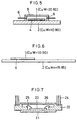
- Figs. 7 and 8 of the accompanying drawings are sectional views showing typical constructions of conventional IC ceramic packages in which the above-described composite materials are used as heat-radiative substrates; and Figs. 9 and 10 are sectional views showing constructions of such packages for use with transistors.
- 21 denotes a substrate composed of CuW or CuMo
- 22 denotes a multi-laminated ceramic substrate composed of, for example, Al 2 O 3 layers
- 23 denotes an Si semiconductor device mounted on the substrate 21
- 24 denotes a Kovar (Fe - 29%Ni - 17%Co) lead wire
- 25 denotes a bonding wire
- 26 denotes a package composed of covar or Al 2 O 3 .
- the construction shown in Fig. 8 is such that the Si semiconductor device 23 mounting portion 21a of the substrate 21 is higher than the construction in Fig. 7. Accordingly, the terminal mounting portion 27 of the multi-laminated ceramic substrate 22 can be flush with the Si semiconductor device 23, thus advantageous for mounting devices.
- Figs. 9 and 10 of the drawings Conventional transistor-oriented packages are now described, referring to Figs. 9 and 10 of the drawings.
- a GaAs transistor device 29 is directly mounted to a protrusive portion 21b provided on a CuW or CuMo heat-radiative substrate 21 having a good heat conductivity and the device can be wired with a circuit 31 provided on an insulating ceramic substrate 30 in the vicinity of the device so as to be flush with the circuit, which type of construction is thus preferred.
- the substrates 21 used in the packages shown in Fig. 7 and Fig. 9 out of the above-described ones are simple flat plates which do not involve much difficulty in manufacture thereof, whereas the stepped substrates having partial protrusions 21a and 21b as shown in Fig. 8 and Fig. 10 involve various problems on manufacture thereof.
- stepped substrates are manufactured, in general, by leaving protrusive portions on a sheet of flat plate and removing the remains thereof by cutting or grinding.
- This method is wasteful in material to be cut and, what is more, burdened with cost for cutting tools due to the fact that its substrate material is of combination of Cu, which is a soft material, and W or Mo, which is a hard, difficult-to-cut material, and therefore the cutting tools are unavoidably subject to intermittent cutting, with the result of their greatly worn edges, which requires cutting tools to be frequently exchanged to obtain high precision and suppress any after-processing machining distortions.
- the substrate 21 used for a package having such a configuration as shown in Fig. 8 is shaped as shown in Fig. 11, where the surface 33 brazed to the ceramic substrate 22 is larger in area than the surface 32 on which the semiconductor device 23 is mounted.
- the surface 33 is often required to be as thin as 0.3 to 0.5 mm, normally.
- the area of the part to be cut off is large and, when the edge of the cutting tool is worn, the mounting surface 33 is deformed due to machining distortion in cutting, thus often encountering an obstacle in brazing it with the ceramic substrate 22.
- one method is that W or Mo powder is molded by die-pressing into a stepped shape similar to the foregoing one and Cu is infiltrated into a porous product obtained by sintering the molding result (the infiltration method).
- Another is that mixed powder of W or Mo powder and Cu powder is molded by die-pressing into a stepped shape similar to the foregoing one and the result is sintered (the mixed powder sintering method).
- the surface 33 to be brazed with the ceramic substrate 22 is thin such that a die-pressing result having the same density as the semiconductor-device mounting surface 32 is difficult to obtain.
- the brazed surface 33 which forms the thin-wall portion of the die-pressing result, is low in strength, thus difficult to treat.
- the heat-radiative substrate 21 used for transistor-oriented packages having a sectional configuration as shown in Fig. 10, is shaped as shown in Fig. 12, where the protrusive portion 21b on which the GaAs transistor device 29 is mounted is much smaller than the flat portion 34.
- the inventors made every effort to solve the foregoing problems of the prior art in obtaining the above-described stepped substrates and packages with the substrates assembled therein, and thus have achieved the present invention.
- the present invention provides a method for manufacturing a semiconductor-mounting heat-radiative substrate, which is a joined body of a CuW or a CuMo composite metal alloy with a layer of copper, free of empty holes, interposed therebetween, comprising the step of joining together a plurality of CuW or CuMo composite metal alloys obtained by either
- the invention also provides a semiconductor-package comprising a heat-radiative substrate made by a method as defined above and enclosure members mounted on said substrate, wherein the thermal expansion coefficient of each composite metal alloy portion of said substrate closely match with that of an enclosure member adjacent to said portion.
- a flat plate 1 serving as the stepped protrusive portion, as shown in Fig. 1, and a flat plate 2 forming the flat portion are separately prepared.
- the melted Cu foil melts with the Cu contained in the composite metal alloy, any excess thereof being press-formed out of the joint surface.
- the brazing material used for joining ceramic substrates in assembling packages generally, eutectic brazing material, brazing temperature: 750 to 900 °C
- the remaining empty holes of the joint surface which is in question, are free from any defects as in the inside of the metal alloy manufactured by the infiltration method, since the melted Cu foil and Cu contained in the composite metal alloy are integrated together so that the excessive part thereof covers the entire joint surface, thus excluding any problems.
- the method of the present invention is advantageous not only in saving the materials for the composite metal alloys to be used and reducing the costs for the cutting process and the tools due to reduction in cutting-processed margins but also in capability of making a number of shapes by combinations by means of preparing simple standard dies. Thus, it is suitable for manufacturing such products which are critical to meet the need for various-type, small-lot production.
- the method of the present invention can provide substrates having the following advantages on performance in addition to the above-described ones on manufacture.
- the joining method of the present invention it is possible to vary the composition ratio of materials combined thereby to make substrates having such characteristics that cannot be provided by the method of grinding out them from a single material by cutting.
- CuW or CuMo composite metal alloys have the following characteristics depending on their composition.
- composition ratio as shown below are available depending on the type of insulating materials and electrically conductive materials to be used in combination:
- a CuMo composite metal alloy although its heat conductivity is inferior to that of CuW composite materials, is small in specific gravity, thus suitable for use as substrates for large-sized packages.
- thermal characteristics heat conductivity and thermal expansion ratio
- ceramic packages used as substrates for use in Si FET-oriented ceramic packages, where good thermal and insulating characteristics are required, are ceramic packages of such a construction that Al 2 O 3 is used as the multi-layer insulating ceramic substrate 22 of outer walls and BeO is used as the heat-radiative insulating circuit substrate 28 on which the semiconductor device 23 is mounted, as shown in Fig. 9.
- the combinational substrates of different composition ratios made by the method of the present invention have a soft Cu thin layer existing between the two materials, and this thin layer serves as a buffer layer so that almost no deformation will occur due to the difference in thermal expansion ratios of the two materials.
- reference numeral 5 denotes an outer frame made of Kovar or the like
- 6 denotes a covar lead wire
- 7 denotes a glass seal.
- a 9 mm ⁇ 9 mm ⁇ 0.1 mm Cu plate 4 was set within a carbon jig, and heated at 1200 °C for 10 minutes in a hydrogen atmosphere to melt Cu. Thereafter, it was cooled. Thus, a stepped heat-radiative substrates as shown in Fig. 6 was obtained. After the Cu adhering to the periphery of joint portion was cut away, it was ground by barrel finishing to eliminate the Cu adhering to the periphery.
- the resulting package proved to have no cracking in the beryllia plate and moreover the warp of the bottom surface of the package was less than 0.002 mm. Thus, a package having a successful heat radiation characteristic was obtained.
- This die-pressed product was heated at 500°C in a hydrogen atmosphere to remove the camphor, and then sintered at 1200 °C for 2 hours in a hydrogen atmosphere. Thus, an Mo porous product was obtained.
- a plurality of CuW or CuMo materials having different compositions and made by the infiltration method or the mixed powder sintering method are joined together with a Cu plate or foil interposed therebetween, and as a result thereof, the remaining empty holes within the CuW or CuMo material are filled with melted Cu, thus allowing heat-radiative substrates excellent in performance to be obtained.
Claims (4)
- Verfahren zum Herstellen eines wärmestrahlenden Substrats zum Montieren von Halbleitern, das ein Verbundkörper aus einer CuW- oder einer CuMo-Verbundmetallegierung mit einer Schicht Kupfer (4), frei von dazwischenliegenden leeren Löchern, ist, umfassend den Schritt des Verbindens einer Mehrzahl von CuW- oder CuMo-Verbundmetallegierungen (1, 2), die entweder erhalten werden durchwobei eine Cu-Schicht an einer Grenzfläche zwischen den CuW- oder CuMo-Verbundmetallegierungen angeordnet wird und die Mehrzahl von CuW- oder CuMo-Verbundmetallegierungen durch Cu (4) verbunden werden, indem sie über den Schmelzpunkt von Cu in einer reduzierenden Atmosphäre erwärmt werden.(a) ein Infiltrationsverfahren, in dem W- oder Mo-Pulver geformt wird und dann geschmolzenes Cu in einer reduzierenden Atmosphäre in leere Löcher eines porösen Produkts, das durch Sintem des Ergebnisses erhalten wird, infiltriert wird, oder(b) ein Mischpulversinterverfahren, wobei W- oder Mo-Pulver mit Cu-Pulver gemischt und geformt wird, bei einer Temperatur über dem Schmelzpunkt von Cu behandelt wird, um eine Verbundmetallegierung zu erhalten,
- Verfahren nach Anspruch 1, wobei eine Mehrzahl von CuW- oder CuMo-Verbundmetallegierungen (1, 2) verwendet werden, die gegenüber den genannten CuW- oder CuMo-Verbundmetallegierungen eine unterschiedliche Zusammensetzung aufweisen.
- Verfahren nach Anspruch 1 oder Anspruch 2, wobei die reduzierende Atmosphäre eine Wasserstoffatmosphäre ist.
- Halbleiterpackung, umfassend ein wärmestrahlendes Substrat, das durch ein Verfahren nach einem der vorangehenden Ansprüche hergestellt wurde.
Applications Claiming Priority (2)
| Application Number | Priority Date | Filing Date | Title |
|---|---|---|---|
| JP29009290 | 1990-10-26 | ||
| JP290092/90 | 1990-10-26 |
Publications (3)
| Publication Number | Publication Date |
|---|---|
| EP0482812A2 EP0482812A2 (de) | 1992-04-29 |
| EP0482812A3 EP0482812A3 (en) | 1992-05-20 |
| EP0482812B1 true EP0482812B1 (de) | 1998-01-07 |
Family
ID=17751696
Family Applications (1)
| Application Number | Title | Priority Date | Filing Date |
|---|---|---|---|
| EP91309470A Expired - Lifetime EP0482812B1 (de) | 1990-10-26 | 1991-10-15 | Verfahren zum Herstellen von wärmestrahlender Substraten zum Montieren von Halbleitern und gemäss diesem Verfahren hergestellte Halbleiterpackung |
Country Status (4)
| Country | Link |
|---|---|
| US (2) | US5305947A (de) |
| EP (1) | EP0482812B1 (de) |
| JP (1) | JPH053265A (de) |
| DE (1) | DE69128601T2 (de) |
Families Citing this family (15)
| Publication number | Priority date | Publication date | Assignee | Title |
|---|---|---|---|---|
| JP3362530B2 (ja) * | 1993-12-16 | 2003-01-07 | セイコーエプソン株式会社 | 樹脂封止型半導体装置およびその製造方法 |
| JP3493833B2 (ja) * | 1995-10-09 | 2004-02-03 | 住友電気工業株式会社 | 半導体素子搭載用プラスチックパッケージおよびその製造方法 |
| US5798566A (en) * | 1996-01-11 | 1998-08-25 | Ngk Spark Plug Co., Ltd. | Ceramic IC package base and ceramic cover |
| JP2833592B2 (ja) * | 1996-08-09 | 1998-12-09 | 日本電気株式会社 | 半導体容器 |
| JP3814924B2 (ja) * | 1997-04-03 | 2006-08-30 | 住友電気工業株式会社 | 半導体装置用基板 |
| US6271585B1 (en) * | 1997-07-08 | 2001-08-07 | Tokyo Tungsten Co., Ltd. | Heat sink substrate consisting essentially of copper and molybdenum and method of manufacturing the same |
| KR100481926B1 (ko) * | 1997-10-31 | 2005-08-29 | 삼성전자주식회사 | 일반칩형반도체패키지및플립칩형반도체패키지와그제조방법 |
| JP2003152145A (ja) | 2001-08-31 | 2003-05-23 | Sumitomo Electric Ind Ltd | 半導体放熱用基板とその製造方法及びパッケージ |
| AT5972U1 (de) * | 2002-03-22 | 2003-02-25 | Plansee Ag | Package mit substrat hoher wärmeleitfähigkeit |
| JP4799069B2 (ja) * | 2005-07-28 | 2011-10-19 | Jfe精密株式会社 | 電子機器で用いる放熱板 |
| EP2071620A1 (de) | 2007-12-12 | 2009-06-17 | Wen-Long Chyn | Kühlkörper mit erweiterter Wärmeverstärkungskapazität |
| US10347559B2 (en) | 2011-03-16 | 2019-07-09 | Momentive Performance Materials Inc. | High thermal conductivity/low coefficient of thermal expansion composites |
| JP6650958B2 (ja) * | 2012-04-27 | 2020-02-19 | キヤノン株式会社 | 電子部品、電子モジュールおよびこれらの製造方法 |
| CN103706797B (zh) * | 2013-12-25 | 2016-08-24 | 西安理工大学 | 宽幅多层Cu-CuMo70-Cu复合材料的制备方法 |
| US9559026B2 (en) | 2015-02-26 | 2017-01-31 | Infineon Technologies Americas Corp. | Semiconductor package having a multi-layered base |
Family Cites Families (20)
| Publication number | Priority date | Publication date | Assignee | Title |
|---|---|---|---|---|
| US3787958A (en) * | 1965-08-18 | 1974-01-29 | Atomic Energy Commission | Thermo-electric modular structure and method of making same |
| FR2431900A1 (fr) * | 1978-07-25 | 1980-02-22 | Thomson Csf | Systeme de soudure d'un laser a semiconducteur sur un socle metallique |
| US4451540A (en) * | 1982-08-30 | 1984-05-29 | Isotronics, Inc. | System for packaging of electronic circuits |
| EP0113088B1 (de) * | 1982-12-22 | 1989-05-24 | Sumitomo Electric Industries Limited | Trägersubstrat für Halbleiterelement |
| JPS6088438A (ja) * | 1983-10-21 | 1985-05-18 | Nec Corp | 半導体装置の製造方法 |
| US4649416A (en) * | 1984-01-03 | 1987-03-10 | Raytheon Company | Microwave transistor package |
| US4563383A (en) * | 1984-03-30 | 1986-01-07 | General Electric Company | Direct bond copper ceramic substrate for electronic applications |
| EP0216090A1 (de) * | 1985-08-30 | 1987-04-01 | Siemens Aktiengesellschaft | Gehäuse für ein im Betrieb Verlustwärme abgebendes Schaltungsbauteil |
| JPH088321B2 (ja) * | 1987-01-19 | 1996-01-29 | 住友電気工業株式会社 | 集積回路パツケ−ジ |
| US4757934A (en) * | 1987-02-06 | 1988-07-19 | Motorola, Inc. | Low stress heat sinking for semiconductors |
| US4736883A (en) * | 1987-02-25 | 1988-04-12 | Gte Products Corporation | Method for diffusion bonding of liquid phase sintered materials |
| CA1284536C (en) * | 1987-07-03 | 1991-05-28 | Akira Sasame | Member for semiconductor apparatus |
| DE3924225C2 (de) * | 1988-07-22 | 1994-01-27 | Mitsubishi Electric Corp | Verfahren zur Herstellung eines Keramik-Metall-Verbundsubstrats sowie Keramik-Metall-Verbundsubstrat |
| JPH02146748A (ja) * | 1988-11-28 | 1990-06-05 | Nec Corp | 半導体容器 |
| EP0382203B1 (de) * | 1989-02-10 | 1995-04-26 | Fujitsu Limited | Keramische Packung vom Halbleiteranordnungstyp und Verfahren zum Zusammensetzen derselben |
| EP0412528A3 (en) * | 1989-08-11 | 1993-01-20 | Fujitsu Limited | Electronic circuit package and production thereof |
| JP2978511B2 (ja) * | 1989-09-20 | 1999-11-15 | 株式会社日立製作所 | 集積回路素子実装構造体 |
| US5100740A (en) * | 1989-09-25 | 1992-03-31 | General Electric Company | Direct bonded symmetric-metallic-laminate/substrate structures |
| JPH04348062A (ja) * | 1991-01-09 | 1992-12-03 | Sumitomo Electric Ind Ltd | 半導体搭載用放熱基板の製造法と該基板を用いた半導体用パッケージ |
| JPH04333265A (ja) * | 1991-05-08 | 1992-11-20 | Sumitomo Electric Ind Ltd | 半導体放熱基板材料の製造方法 |
-
1991
- 1991-10-15 EP EP91309470A patent/EP0482812B1/de not_active Expired - Lifetime
- 1991-10-15 DE DE69128601T patent/DE69128601T2/de not_active Expired - Fee Related
- 1991-10-28 JP JP3309934A patent/JPH053265A/ja active Pending
-
1993
- 1993-07-07 US US08/087,073 patent/US5305947A/en not_active Expired - Fee Related
-
1994
- 1994-01-13 US US08/181,313 patent/US5451817A/en not_active Expired - Fee Related
Also Published As
| Publication number | Publication date |
|---|---|
| US5451817A (en) | 1995-09-19 |
| JPH053265A (ja) | 1993-01-08 |
| EP0482812A2 (de) | 1992-04-29 |
| US5305947A (en) | 1994-04-26 |
| EP0482812A3 (en) | 1992-05-20 |
| DE69128601D1 (de) | 1998-02-12 |
| DE69128601T2 (de) | 1998-06-04 |
Similar Documents
| Publication | Publication Date | Title |
|---|---|---|
| EP0482812B1 (de) | Verfahren zum Herstellen von wärmestrahlender Substraten zum Montieren von Halbleitern und gemäss diesem Verfahren hergestellte Halbleiterpackung | |
| US6917638B2 (en) | Heat radiator for electronic device and method of making it | |
| US5886407A (en) | Heat-dissipating package for microcircuit devices | |
| US7180178B2 (en) | Semiconductor heat-dissipating substrate, and manufacturing method and package therefor | |
| US5481136A (en) | Semiconductor element-mounting composite heat-sink base | |
| EP1432029A2 (de) | Halbleiterchipgehäuse mit einem Metall-diamant-verbundmaterial im Substrat, und dessen Herstellungsverfahren | |
| EP1255297B1 (de) | Elektrisch isolierte Einkapselung eines Leistungsbauteils | |
| US20040183172A1 (en) | Package for housing semiconductor chip, and semiconductor device | |
| KR20030028462A (ko) | 고강도 다층 반도체 패키지 및 그 제조 방법 | |
| US5188985A (en) | Surface mount device with high thermal conductivity | |
| KR20010079642A (ko) | 복합 재료 및 그를 이용한 반도체 장치 | |
| JP3856640B2 (ja) | 半導体搭載用放熱基板材料、その製造方法、及びそれを用いたセラミックパッケージ | |
| US20020191377A1 (en) | Material of heat-dissipating plate on which semiconductor is mounted, method for fabricating the same, and ceramic package produced by using the same | |
| EP1231633B1 (de) | Material für eine wärme-abführende platte auf der ein halbleiter montiert ist, herstellungsmethode und keramisches gehäuse,produziert unter verwendung derselben | |
| JPH04348062A (ja) | 半導体搭載用放熱基板の製造法と該基板を用いた半導体用パッケージ | |
| KR100413848B1 (ko) | 광모듈용 밀폐형 패키지 | |
| JPH05211248A (ja) | 半導体搭載用複合放熱基板及びその製造方法 | |
| WO2022162871A1 (ja) | 両面冷却パワーモジュール | |
| JPH0340453A (ja) | 高周波高出力トランジスターパッケージ | |
| JP2004200530A (ja) | 半導体素子収納用パッケージおよび半導体装置 | |
| JP2000147332A (ja) | 光半導体用パッケージおよびその製造方法 | |
| JP2002246710A (ja) | ベース板一体型セラミックス回路基板とその製法 | |
| JPH0340454A (ja) | ピン、グリッドアレイパッケージ |
Legal Events
| Date | Code | Title | Description |
|---|---|---|---|
| PUAI | Public reference made under article 153(3) epc to a published international application that has entered the european phase |
Free format text: ORIGINAL CODE: 0009012 |
|
| PUAL | Search report despatched |
Free format text: ORIGINAL CODE: 0009013 |
|
| AK | Designated contracting states |
Kind code of ref document: A2 Designated state(s): DE FR GB IT NL |
|
| AK | Designated contracting states |
Kind code of ref document: A3 Designated state(s): DE FR GB IT NL |
|
| 17P | Request for examination filed |
Effective date: 19921005 |
|
| 17Q | First examination report despatched |
Effective date: 19941012 |
|
| GRAG | Despatch of communication of intention to grant |
Free format text: ORIGINAL CODE: EPIDOS AGRA |
|
| GRAG | Despatch of communication of intention to grant |
Free format text: ORIGINAL CODE: EPIDOS AGRA |
|
| GRAH | Despatch of communication of intention to grant a patent |
Free format text: ORIGINAL CODE: EPIDOS IGRA |
|
| GRAH | Despatch of communication of intention to grant a patent |
Free format text: ORIGINAL CODE: EPIDOS IGRA |
|
| GRAA | (expected) grant |
Free format text: ORIGINAL CODE: 0009210 |
|
| AK | Designated contracting states |
Kind code of ref document: B1 Designated state(s): DE FR GB IT NL |
|
| PG25 | Lapsed in a contracting state [announced via postgrant information from national office to epo] |
Ref country code: IT Free format text: LAPSE BECAUSE OF FAILURE TO SUBMIT A TRANSLATION OF THE DESCRIPTION OR TO PAY THE FEE WITHIN THE PRE;WARNING: LAPSES OF ITALIAN PATENTS WITH EFFECTIVE DATE BEFORE 2007 MAY HAVE OCCURRED AT ANY TIME BEFORE 2007. THE CORRECT EFFECTIVE DATE MAY BE DIFFERENT FROM THE ONE RECORDED.SCRIBED TIME-LIMIT Effective date: 19980107 Ref country code: NL Free format text: LAPSE BECAUSE OF FAILURE TO SUBMIT A TRANSLATION OF THE DESCRIPTION OR TO PAY THE FEE WITHIN THE PRESCRIBED TIME-LIMIT Effective date: 19980107 |
|
| REF | Corresponds to: |
Ref document number: 69128601 Country of ref document: DE Date of ref document: 19980212 |
|
| ET | Fr: translation filed | ||
| NLV1 | Nl: lapsed or annulled due to failure to fulfill the requirements of art. 29p and 29m of the patents act | ||
| PLBE | No opposition filed within time limit |
Free format text: ORIGINAL CODE: 0009261 |
|
| STAA | Information on the status of an ep patent application or granted ep patent |
Free format text: STATUS: NO OPPOSITION FILED WITHIN TIME LIMIT |
|
| 26N | No opposition filed | ||
| PGFP | Annual fee paid to national office [announced via postgrant information from national office to epo] |
Ref country code: FR Payment date: 19991011 Year of fee payment: 9 |
|
| PGFP | Annual fee paid to national office [announced via postgrant information from national office to epo] |
Ref country code: GB Payment date: 19991013 Year of fee payment: 9 |
|
| PGFP | Annual fee paid to national office [announced via postgrant information from national office to epo] |
Ref country code: DE Payment date: 19991018 Year of fee payment: 9 |
|
| PG25 | Lapsed in a contracting state [announced via postgrant information from national office to epo] |
Ref country code: GB Free format text: LAPSE BECAUSE OF NON-PAYMENT OF DUE FEES Effective date: 20001015 |
|
| GBPC | Gb: european patent ceased through non-payment of renewal fee |
Effective date: 20001015 |
|
| PG25 | Lapsed in a contracting state [announced via postgrant information from national office to epo] |
Ref country code: FR Free format text: LAPSE BECAUSE OF NON-PAYMENT OF DUE FEES Effective date: 20010629 |
|
| PG25 | Lapsed in a contracting state [announced via postgrant information from national office to epo] |
Ref country code: DE Free format text: LAPSE BECAUSE OF NON-PAYMENT OF DUE FEES Effective date: 20010703 |
|
| REG | Reference to a national code |
Ref country code: FR Ref legal event code: ST |