EP0477884B1 - Circuit pour l'interpolation de lignes horizontales et dispositifs de prise d'image le comportant - Google Patents
Circuit pour l'interpolation de lignes horizontales et dispositifs de prise d'image le comportant Download PDFInfo
- Publication number
- EP0477884B1 EP0477884B1 EP91116300A EP91116300A EP0477884B1 EP 0477884 B1 EP0477884 B1 EP 0477884B1 EP 91116300 A EP91116300 A EP 91116300A EP 91116300 A EP91116300 A EP 91116300A EP 0477884 B1 EP0477884 B1 EP 0477884B1
- Authority
- EP
- European Patent Office
- Prior art keywords
- signal
- circuit
- interpolation
- lines
- output
- Prior art date
- Legal status (The legal status is an assumption and is not a legal conclusion. Google has not performed a legal analysis and makes no representation as to the accuracy of the status listed.)
- Expired - Lifetime
Links
Images


Classifications
-
- G—PHYSICS
- G06—COMPUTING OR CALCULATING; COUNTING
- G06T—IMAGE DATA PROCESSING OR GENERATION, IN GENERAL
- G06T3/00—Geometric image transformations in the plane of the image
- G06T3/40—Scaling of whole images or parts thereof, e.g. expanding or contracting
- G06T3/4007—Scaling of whole images or parts thereof, e.g. expanding or contracting based on interpolation, e.g. bilinear interpolation
-
- G—PHYSICS
- G06—COMPUTING OR CALCULATING; COUNTING
- G06F—ELECTRIC DIGITAL DATA PROCESSING
- G06F17/00—Digital computing or data processing equipment or methods, specially adapted for specific functions
- G06F17/10—Complex mathematical operations
- G06F17/17—Function evaluation by approximation methods, e.g. inter- or extrapolation, smoothing, least mean square method
-
- H—ELECTRICITY
- H04—ELECTRIC COMMUNICATION TECHNIQUE
- H04N—PICTORIAL COMMUNICATION, e.g. TELEVISION
- H04N23/00—Cameras or camera modules comprising electronic image sensors; Control thereof
- H04N23/80—Camera processing pipelines; Components thereof
- H04N23/84—Camera processing pipelines; Components thereof for processing colour signals
- H04N23/843—Demosaicing, e.g. interpolating colour pixel values
-
- H—ELECTRICITY
- H04—ELECTRIC COMMUNICATION TECHNIQUE
- H04N—PICTORIAL COMMUNICATION, e.g. TELEVISION
- H04N5/00—Details of television systems
- H04N5/14—Picture signal circuitry for video frequency region
- H04N5/20—Circuitry for controlling amplitude response
- H04N5/205—Circuitry for controlling amplitude response for correcting amplitude versus frequency characteristic
- H04N5/208—Circuitry for controlling amplitude response for correcting amplitude versus frequency characteristic for compensating for attenuation of high frequency components, e.g. crispening, aperture distortion correction
-
- H—ELECTRICITY
- H04—ELECTRIC COMMUNICATION TECHNIQUE
- H04N—PICTORIAL COMMUNICATION, e.g. TELEVISION
- H04N5/00—Details of television systems
- H04N5/14—Picture signal circuitry for video frequency region
- H04N5/21—Circuitry for suppressing or minimising disturbance, e.g. moiré or halo
-
- H—ELECTRICITY
- H04—ELECTRIC COMMUNICATION TECHNIQUE
- H04N—PICTORIAL COMMUNICATION, e.g. TELEVISION
- H04N5/00—Details of television systems
- H04N5/222—Studio circuitry; Studio devices; Studio equipment
- H04N5/262—Studio circuits, e.g. for mixing, switching-over, change of character of image, other special effects ; Cameras specially adapted for the electronic generation of special effects
- H04N5/2628—Alteration of picture size, shape, position or orientation, e.g. zooming, rotation, rolling, perspective, translation
-
- H—ELECTRICITY
- H04—ELECTRIC COMMUNICATION TECHNIQUE
- H04N—PICTORIAL COMMUNICATION, e.g. TELEVISION
- H04N2209/00—Details of colour television systems
- H04N2209/04—Picture signal generators
- H04N2209/041—Picture signal generators using solid-state devices
- H04N2209/042—Picture signal generators using solid-state devices having a single pick-up sensor
- H04N2209/045—Picture signal generators using solid-state devices having a single pick-up sensor using mosaic colour filter
- H04N2209/046—Colour interpolation to calculate the missing colour values
-
- H—ELECTRICITY
- H04—ELECTRIC COMMUNICATION TECHNIQUE
- H04N—PICTORIAL COMMUNICATION, e.g. TELEVISION
- H04N25/00—Circuitry of solid-state image sensors [SSIS]; Control thereof
- H04N25/10—Circuitry of solid-state image sensors [SSIS]; Control thereof for transforming different wavelengths into image signals
- H04N25/11—Arrangement of colour filter arrays [CFA]; Filter mosaics
- H04N25/13—Arrangement of colour filter arrays [CFA]; Filter mosaics characterised by the spectral characteristics of the filter elements
- H04N25/135—Arrangement of colour filter arrays [CFA]; Filter mosaics characterised by the spectral characteristics of the filter elements based on four or more different wavelength filter elements
- H04N25/136—Arrangement of colour filter arrays [CFA]; Filter mosaics characterised by the spectral characteristics of the filter elements based on four or more different wavelength filter elements using complementary colours
Definitions
- the present invention relates to a horizontal line interpolation circuit which functions to increase or decrease the number of horizontal lines through interpolation processing such as electronic zoom function, by which an image is electronically enlarged, or some method conversion, and further relates to an image pickup apparatus provided with a horizontal line interpolation circuit which functions to increase or decrease the number of horizontal lines of a picked-up image through interpolation processing.
- the prior art will be described below taking the case of an image pickup apparatus provided with an image enlargement function which is effected by increasing the number of horizontal lines of an image.
- a horizontal line interpolation circuit is the television standards converter circuit as shown e.g. in EP-A-0 367 418.
- a further typical example is shown in a literature, Journal of the Japanese Television Society, Vol 29., No. 10, pp. 773 to 784, Fig. 3.
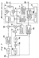
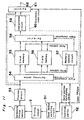
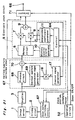
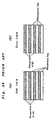
- Shown in Fig. 27 is a typical example of conventional image pickup apparatus which electronically enlarge an image picked-up by an image sensor with application of the above-mentioned horizontal line interpolation circuit.
- reference numeral 1 denotes a solid state image sensor
- 2 denotes a driving circuit for the solid state image sensor 1
- 3 denotes an amplifier for amplifying an output signal from the solid state image sensor 1
- 68 denotes a process circuit for generating a luminance signal or the like from output of the amplifier 3
- 69 denotes a vertical aperture correction signal generator
- 70 denotes a first adder for obtaining a luminance signal whose vertical sharpness has been corrected by adding a luminance signal from the process circuit 68 and a vertical aperture correction signal from the vertical aperture correction signal generator circuit 69.
- Numeral 5 denotes an electronic zoom circuit for enlargement-processing an output signal from the first adder 70 by increasing the number of horizontal lines through interpolation processing
- the electronic zoom circuit 5 generally comprising: a memory circuit 6; a memory control signal generator 10 for generating control signals for write, read, and addresses of the memory circuit 6; multipliers 7, 8 for multiplying signals of two lines read from the memory circuit 6 by their respective interpolation weight coefficients w, (1-w); a second adder 9 for adding up output signals of the multipliers 7, 8 to yield interpolation output; and an interpolation coefficient generator 11 for generating the interpolation weight coefficients w, (1-w) for signals of two lines in accordance with instructions from a control section 64.
- the control section 64 generates control signals to the memory control signal generator 10 and the interpolation coefficient generator 11 according to the zoom multiplying factor of the electronic zoom and the screen position to be zoomed (zoom position).
- Numeral 71 denotes a selector for switching between electronically zoomed output of the electronic zoom circuit 5 and non-zoomed output of the first adder 70 in accordance with instructions from an operation switch 52, which selector 71 feeds a signal to an output terminal 66.
- Numeral 52 denotes an operation switch for giving instructions for on/off control of the electronic zoom as well as the zoom multiplying factor and screen position to be zoomed (zoom position) for the on-control of the electronic zoom.
- the image pickup apparatus so arranged as to perform electronic zoom operation of the same multiplying factor at all times does not require the selector 71 or the operation switch 52; such conventional apparatus is shown in Fig. 28. As shown in the figure, all but the selector 71 and the operation switch 52 of its construction are the same as in Fig. 27.
- the solid state image sensor 1 is scanned by a normal scan method (a scan method corresponding to interlace scan), as shown in Fig. 32. More specifically, signal charge of each pixel of the solid state image sensor 1 is scanned in such a way that for the odd field, as indicated by solid line of Fig. 32, two adjoining horizontal pixel rows are scanned by one-time horizontal scan, while for the even field, as indicated by dotted line of Fig. 32, the two pairs of horizontal pixel rows simultaneously read by one-time horizontal scan are scanned by shifting one row with respect to the odd field in the vertical direction, where of an output signal, the relation between the scanning lines of the odd field and those of the even field is an interlace relation, as shown in Fig. 33 (a).
- solid line represents scanning lines of the odd field
- dotted line represents those of the even field.
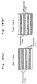
- FIG. 29 Shown in Fig. 29 is a conceptual view of the image enlargement with the above-described image enlarging apparatus. Now assume that the solid state image sensor 1 puts out an image of 240 lines for one field and therefore 480 lines for one frame.
- the electronic zoom circuit 5 in Fig. 27 performs an interpolation processing as shown in Fig. 30 (a).
- an interpolation processing as shown in Fig. 30 (a).
- input lines of the n th and (n+1) th lines are read from the memory circuit 6 and multiplied by interpolation weight coefficients relative to distances (here, 2/12 and 10/12), then added together.
- other output lines are also obtained from the upper and lower two lines by multiplying interpolation weight coefficients relative to distances and adding together.
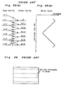
- vertical frequency response characteristic of the output signal obtained by the interpolation processing is examined.
- a line interpolated with interpolation weight coefficients of 1/2 and 1/2 results in the perfect average of input two lines, causing the vertical frequency response characteristic to be the lowest, while a line interpolated with interpolation weight coefficients of 1 and 0 allows one line of an input signal to be output as it is, causing the frequency response characteristic to be the highest.
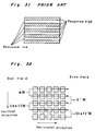
- each output line can be graphed as shown in Fig. 30 (b).
- the graph shows that the lines are either high or low in vertical frequency response, causing high and low portions in vertical frequency response to take place on the output screen, as shown in Fig. 31.
- the electronic zoom circuit 5 in Fig. 27 performs an interpolation processing as shown in Fig. 33 (a). More specifically, odd field output lines are obtained in the odd field from odd field input lines in Fig. 33 (a), while even field output lines are obtained in the even field from even field input lines in the same figure (a). For example, to obtain the (N+1) th line of the odd field, input lines n and n+1 are read from the memory circuit 6, multiplied by interpolation weight coefficients relative to distances (in this case, 2/12 and 10/12), and added together. Similarly, other output lines are also obtained from the upper and lower two lines by multiplying interpolation weight coefficients relative to distances and adding together.
- the vertical noise characteristic of an output signal obtained by the interpolation processing also results in that interpolated line is the perfect average of two input lines, as in the above-described cases, when the lines are interpolated with interpolation weight coefficients of 1/2 and 1/2. Accordingly, the resulting S/N ratio is improved by 3 dB at a maximum, hence a satisfactory S/N ratio.
- the noise level characteristic for each output line can be graphed as shown in Fig. 35 (b). This indicates that an electronically zoomed output image has different S/N ratios of lines, causing noise differences between lines to be viewed as disturbing lateral stripes in the output image, as shown in Fig. 36.
- the conventional horizontal line interpolation circuit as described above has the following problem.
- the vertical frequency response characteristic of an output line varies with interpolation weight coefficient and therefore differ between output lines.
- the output screen involves high and low portions in vertical frequency response, causing the vertical frequency response of an image to be diverse to a great extent depending on the vertical positions of the screen. This results in a most undesirable, unfriendly-to-see image, disadvantageously.
- the image enlarging apparatus and the image pickup apparatus which perform conventional electronic zoom as described above, as stated above, involve different S/N ratios of lines in an electronically zoomed output image, which appear as disturbing lateral stripes in an output image. Accordingly, in common image enlarging apparatus, especially when input signal level is such low as to require the gain of a gain control amplifier to be increased, the S/N ratio of a signal entered into the electronic zoom circuit is unsatisfactory with disturbing lateral stripes conspicuously present.
- the S/N ratio of a signal entered into the electronic zoom circuit is unsatisfactory, causing the disturbing lateral stripes to be conspicuously present.
- the present invention has been developed with a view to substantially solving the above described disadvantages and has for its essential object to provide an improved horizontal line interpolation circuit and an image pickup apparatus with horizontal line interpolation function in which vertical frequency response of an image will not vary with vertical positions of the screen.
- the present invention has for its another important object to provide a horizontal line interpolation circuit and an image pickup apparatus with horizontal line interpolation function which are reduced in disturbing lateral stripes due to S/N difference between lines of the screen.
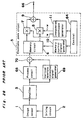
- Fig. 1 is a block diagram showing a first embodiment of the first apparatus of the present invention. Referring to the figure, its construction and operation is explained.
- reference numeral 1 denotes an image sensor
- 2 denotes a driving circuit for the image sensor 1
- 3 denotes an amplifier for amplifying an output signal from the image sensor 1
- 4 denotes a process circuit for generating luminance signals and others from output of the amplifier 3.
- Numeral 5 denotes an electronic zoom circuit for enlargement-processing an output signal from the process circuit 4 through horizontal line interpolation processing, the electronic zoom circuit 5 generally comprising: a memory circuit 6; a memory control signal generator 10 for generating control signals for write, read, and addresses of the memory circuit 6; multipliers 7, 8 for multiplying signals of two lines read from the memory circuit 6 by their respective interpolation weight coefficients w, (1-w); an adder 9 for adding up output signals of the multipliers 7, 8 to yield interpolation output; and an interpolation coefficient generator 11 for generating the interpolation weight coefficients w, (1-w) for signals of two lines in accordance with instructions from a control section 12.
- the control section 12 controls the zoom multiplying factor of the electronic zoom and the screen position to be zoomed (zoom position).
- Numeral 13 denotes a vertical aperture correction circuit for performing vertical aperture correction for output image signals of the electronic zoom circuit 5, the vertical aperture correction circuit 13 serving to feed a signal to an output terminal 19.
- the vertical aperture correction circuit 13 comprises: a vertical aperture correction signal generator 15 for generating a vertical aperture correction signal out of a signal from the electronic zoom circuit 5; a control signal generator circuit 17 for generating a control signal k according to the interpolation coefficient w of the electronic zoom circuit 5; a third multiplier 16 for controlling the level of a vertical aperture correction signal according to the control signal k; a process circuit 14 for performing delay processing and the like to a signal from the electronic zoom circuit 5; and a second adder 18 for adding up a signal from the process circuit 14 and that from the third multiplier 16 thereby to obtain an image signal having been controlled for the level of vertical aperture correction according to the interpolation coefficient w of the electronic zoom circuit 5.
- the operation of the electronic zoom circuit 5 is the same as in the conventional counterpart in Fig. 27 and thus omitted in the following description, and below described in detail is the operation of the vertical aperture correction circuit 13.
- the control signal generator 17 forms a control signal k that depends on the interpolation weight coefficient w from the interpolation coefficient generator 11 (the signal takes a value proportional to the coefficient w when the w is less than 0.5 and proportional to that of (1-w) when the w is more than 0.5, as shown in Fig. 2), and then a vertical aperture correction signal generated by the vertical aperture correction signal generator 15 is multiplied by the control signal k by the multiplier 16, thus controlling the level of the vertical aperture correction signal.
- output of the multiplier 16 is added to a signal of the process circuit 14 (signal not subjected to vertical aperture correction) by the adder 18, so that a signal adaptively controlled in vertical sharpness according to the interpolation weight coefficient w is fed to the output terminal 19. More specifically, lines having smaller coefficients of either of the interpolation weight coefficient w or (1-w), whichever smaller, that is, those having greater vertical frequency responses as described in the section for the prior art are controlled so as to lower the level of vertical aperture correction signals, while lines having greater coefficients of either of the interpolation weight coefficient w or (1-w), whichever smaller, that is, those having smaller vertical frequency responses as described in the section for the prior art are controlled so as to heighten the level of vertical aperture correction signals.
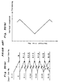
- Fig. 3 is a chart showing the vertical responses of lines of an image, similar to that shown in Fig. 30 (b).
- dotted curve represents the characteristic of the prior art, while solid curve does the characteristic obtained at the output terminal 19 after effecting adaptive control to the level of vertical aperture correction (controlled according to the interpolation weight coefficient w) by the vertical aperture correction circuit 13 of the present invention in Fig. 1.
- a zoom-processed image signal (waveform (a) in Fig. 5) input to an image signal input terminal 20 is delayed by a first one horizontal-scan-period delay circuit (hereinafter, referred to as 1H delay circuit) 22 and a second 1H delay circuit 23 thereby to obtain a 1H delay signal and a 2H delay signal, respectively (waveforms (b) and (c) in Fig. 5).
- 1H delay circuit first one horizontal-scan-period delay circuit
- a control input terminal 21 has the interpolation weight coefficient w led thereto, and the control signal generator 17 generates a control signal k that varies depending on the interpolation weight coefficient w as shown in Fig. 2. Then, the vertical aperture correction signal (waveform (e) in Fig. 5) is multiplied by the control signal k by a multiplier 27, thus controlling the level of the vertical aperture correction signal.
- Output of the multiplier 27 is added to the output signal of the first 1H delay circuit 22 (1H delay signal, waveform (b) in Fig. 5) by a second adder 28, so that a signal whose vertical sharpness has adaptively been controlled according to the interpolation weight coefficient w (waveform (f) in Fig. 5) is fed to an output terminal 29. Consequently, a block 31 in Fig. 4 corresponds to the process circuit 14 in Fig. 1, and a block 30 in Fig. 4 corresponds to the vertical aperture correction signal generator 15 in Fig. 15.
- the vertical aperture correction circuit 13 when the vertical aperture correction circuit 13 is disposed behind the electronic zoom circuit 5 that enlargement-processes an input signal through horizontal line interpolation, there are some advantages: that is, the vertical aperture correction can be effected at a stage at which the number of horizontal lines has been increased by interpolation processing, allowing aperture correction to be effected at higher vertical frequencies with the result of more increased vertical sharpness; the horizontal line of a signal subject to vertical aperture correction and the interpolation weight coefficient w correspond to each other at one to one (as apparent from Fig. 13 (a), the interpolation weight coefficient w is inherent to output line Nos., not corresponding to input line Nos. at one to one), thus allowing the level of vertical aperture correction to be accurately controlled according to the interpolation weight coefficient w.
- Fig. 6 is a block diagram showing a second embodiment of the present invention. Its difference from the first embodiment of Fig. 1 exists in that a vertical aperture correction circuit 33 is disposed ahead of the electronic zoom circuit 5, while in the first embodiment the vertical aperture correction circuit 13 is disposed behind the electronic zoom circuit 5 that enlargement-processes an input signal through horizontal line interpolation.
- reference numeral 1 denotes an image sensor
- 2 denotes a driving circuit for the image sensor 1
- 3 denotes an amplifier for amplifying an output signal from the image sensor 1
- 34 denotes a process circuit for generating luminance signals and others from output of the amplifier 3
- 15 denotes a vertical aperture correction signal generator for generating a vertical aperture correction signal
- 17 denotes a control signal generator for generating a control signal k corresponding to the interpolation weight coefficient w of the electronic zoom circuit 5
- 16 denotes a third multiplier for controlling the level of a vertical aperture correction signal according to the control signal k
- 35 denotes a first adder for adding a luminance signal from the process circuit 34 and a vertical aperture correction signal from the vertical aperture correction signal generator 15 thereby to obtain a luminance signal that has been corrected in vertical sharpness.
- the electronic zoom circuit 5 for enlargement-processing an output signal from the first adder 35 by increasing the number of horizontal lines through interpolation processing is identical to the electronic zoom
- the process circuit 4 and the process circuit 14 in Fig. 1 can be integrated in construction, which allows a simplified construction.
- a third embodiment of the first and second apparatus of the present invention is described below.
- Fig. 7 shows a detailed construction of an image pickup apparatus with image enlargement function in which circuit components of a camera process circuit and a vertical aperture correction signal generator are shared.
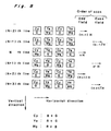
- a signal is led to an input terminal 36 in which a luminance signal and a chrominance signal from the color image sensor provided with such a color filter as shown in Fig. 8 or 9 are synthesized.
- the signal is delayed by a first 1H delay circuit 37 and a second 1H delay circuit 38, thus providing a 1H delay signal and a 2H delay signal, respectively.
- a first adder 39 After adding the input image signal and the 2H delay signal by a first adder 39, the resulting signal multiplied by 1/2 by a 1/2 multiplier circuit 40 is subtracted from the 1H delay signal by a subtracter circuit 41, thereby providing a vertical aperture signal.
- an output signal of the first 1H delay circuit 37 is processed for luminance signal separation and the like by a luminance signal processing circuit 42 so that the luminance signal is extracted.
- the control signal generator 17 generates a control signal k that varies depending on the interpolation weight coefficient w, as shown in Fig. 2, from an electronic zoom circuit 45. Then, the vertical aperture correction signal is multiplied by the control signal k by the multiplier 16, thus controlling the level of the vertical aperture correction signal.
- Output of the multiplier 16 is added to the luminance signal, an output signal of the luminance signal processing circuit 42, by a second adder 43, thereby added to the luminance signal, an interpolation weight coefficient output signal, so that a signal whose vertical sharpness has adaptively been controlled according to the interpolation weight coefficient w is obtained.
- the 1H delay signal and the output of the 1/2 multiplier circuit 40 are both led to a chrominance signal processing circuit 44, where it is processed for color separation, white balance correction, and the like, providing a chrominance signal.
- the luminance signal having adaptively been controlled in vertical sharpness according to the interpolation weight coefficient w, an output of the adder 43, is subjected to horizontal line interpolation by the electronic zoom circuit 45 that comprises: a memory circuit 6; a memory control signal generator 10 for generating control signals for write, read, and addresses of the memory circuit 6; multipliers 7, 8 for multiplying signals of two lines read from the memory circuit 6 by their respective interpolation weight coefficients w, (1-w); a second adder 9 for adding up output signals of the multipliers 7, 8 to feed interpolation output to an output terminal 47; and an interpolation coefficient generator 11 for generating the interpolation weight coefficients w, (1-w) for signals of two lines in compliance with instructions from a control section 12.
- a chrominance signal from the chrominance signal processing circuit 44 is processed for horizontal line interpolation by a chrominance signal interpolation circuit 46, which has a basic construction similar to that for luminance signals, and fed to a chrominance signal output terminal 48.
- an approximate luminance signal of 2R + 3G + 2B as a low-band signal and a color difference signal of 2B - G as a high-frequency modulation signal are obtained from the nH th line or n'H th line
- an approximate luminance signal of 2R + 3G + 2B as a low-band signal and a color difference signal of 2R - G as a high-frequency modulation signal are obtained from the (n+1)H th line or (n+1)'H th line.
- the processing for luminance signal separation is principally carried out by making the signal passed through a low-pass filter.
- the processing for chrominance signal separation is principally done by making a signal from the color image sensor passed through a band-pass filter or by subtraction-processing the signal for each pixel to separate it into two types of color difference signals and further concurrence-processing line-sequential color difference signals using the 1H delay circuit or (1H + 1H) delay circuit.
- the level of vertical aperture correction with luminance signals is adaptively controlled according to the interpolation weight coefficient w as in the first embodiment and others, thus needless to say that differences in vertical frequency response between lines, as would be involved in interpolation processing in the prior arts, can be corrected.
- the first and second apparatus of the present invention have been described above taking the case of an image pickup apparatus provided with image enlargement function (electronic zoom function) through horizontal line interpolation, it is apparent that the present invention can comprehensively be applied to the general horizontal line interpolation circuits without limiting to image pickup apparatus such as described above.
- the image sensor 1 and the driving circuit 2 in Fig. 1 and Fig. 6 are omitted and the amplifier 3 has direct input of an image signal led thereto, and that the process circuit 4 may also be omitted if unnecessary.
- the present invention has been described using a primary interpolation as the horizontal line interpolation method (a method that the mid-point line is obtained out of two adjoining lines, the Sn th and (Sn+1) th line by a calculation of wSn + (1 - w) Sn + 1)
- the interpolation method is not necessarily limited thereto and the present invention can apparently be achieved by any such method if the level of vertical aperture correction is controlled with interpolation weight coefficients according to the method.
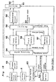
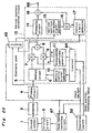
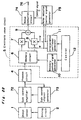
- Fig. 11 is a block diagram of an image pickup apparatus showing a first embodiment of the third apparatus of the present invention.
- reference numeral 1 denotes a solid state image sensor
- 2 denotes a driving circuit for the solid state image sensor 1
- 51 denotes a scan method switching circuit, which is controlled by an electronic zoom on/off control signal from an operation switch 52.
- the operation switch 52 gives instructions for on/off control of the electronic zoom as well as the zoom multiplying factor and screen position to be zoomed (zoom position) for on-control of the electronic zoom.
- Numeral 53 denotes a process circuit for generating luminance signals and chrominance signals from the solid state image sensor 1; 60 denotes an electronic zoom circuit for enlargement-processing an output signal from the process circuit 53, the electronic zoom circuit generally comprising: field memories 55, 56; a switching device 54 for selecting either one of the field memories 55, 56 depending on which field it is, to write a signal; a memory control circuit 57 for putting out write and read addresses for the field memories 55, 56; a selector 58 for selecting either one of the field memories 55, 56 that is not under write operation depending on which field it is, to read a signal; and an interpolation circuit 59 for performing interpolation.
- Designated by numeral 61 is a selector for changing over between electronically zoomed output of an electronic zoom circuit 60 and non-zoomed output of the process circuit 53 in accordance with an instruction from the operation switch 52, the selector 61 serving to feed a signal to an output terminal 62.
- the selector 61 selects a signal from the process circuit 53 according to this control signal to feed a non-zoomed signal to the output terminal 62, while this control signal is also led to the scan method switching circuit 51, controlling so as to scan the solid state image sensor 1 by the same method as in the prior art as shown in Fig. 32 (scan method 1).
- the signal fed to the output terminal 62 is two-field signals in interlace relation.
- the electronic zoom off control signal is led also to the electronic zoom circuit 60 thereby to stop the operation of the electronic zoom circuit 60, there are produced effects in power saving or the like.
- the selector 61 selects a signal from the electronic zoom circuit 60 to feed an electronically zoomed signal to the output terminal 62 according to the control signal, while the control signal is led also to the scan method switching circuit 51, controlling so as to scan the solid state image sensor 1 by the method as shown in Fig. 12.
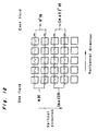
- This scan method is one in which signal charges of pixels of the solid state image sensor are scanned in such a way that the same pair of adjoining two horizontal pixel rows are scanned by one-time horizontal scan for both the odd and even fields, as shown in Fig. 12 (scan method (2)). Accordingly, the two-field signals, output signals of the solid state image sensor 1 are located at an identical position, as shown in Fig. 13 (a).
- the scan lines n, (n+1), (n+2), ... represent scan lines of the odd field
- the scan lines n', (n+1)', (n+2)', ... represent scan lines of the even field.
- the electronic zoom circuit 60 performs the electronic zoom operation as described below.
- the following description is based on the assumption that the solid state image sensor 1 outputs an image of 240 lines for one field, and therefore that of 480 lines for one frame, and that, out of these, a portion corresponding to 200 lines for one field is enlarged so as to obtain a normal one-field image, i.e. a signal of 240 lines.
- the electronic zoom circuit 60 in Fig. 11 performs interpolation processing as shown in Fig. 13 (a). That is, for the odd field, odd field output lines are obtained from odd field input lines in the same manner as in the prior art. For example, to obtain the (N+2) th line in the odd field, the (n+1) th and (n+2) th lines are read from the field memory 55 or 56, the readouts being multiplied by interpolation weight coefficients relative to distances (in this case, 4/12 and 8/12) and further added together. Likewise those for other output lines can be obtained by multiplying readouts of upper and lower two lines by interpolation weight coefficients relative to distances and further adding together.
- even field output lines are obtained from even field input lines in Fig. 13 (a) (the same as input of the odd field) through the same interpolation processing, where the processing is carried out so that lines obtained by the interpolation processing are in interlace relation with signals of the odd field, that is, fall just in the intermediate point between adjoining two lines of the odd field.
- the (n+1)' th and (n+2)' th input lines are read from the field memory 55 or 56 and the readouts are multiplied by the interpolation weight coefficients (in this case, 11/12 and 1/12) relative to distances of the intermediate point between the (N+2) th line and the (N+3) th line of the odd field and further added together.
- the vertical frequency response characteristic of the output signal interpolation-processed as above is such that, as in the prior art, a line interpolated with interpolation weight coefficients of 1/2 and 1/2 results in the perfect average of input two lines, causing the vertical frequency response characteristic to be the lowest, while a line interpolated with interpolation weight coefficients of 1 and 0 allows one line of input 0 to be output as it is, causing the frequency response characteristic to be the highest, whereas the interpolation weight coefficients of adjoining lines between the odd and even fields are not equal and therefore, for example, when lines of the odd field are interpolated with the interpolation weight coefficients of approximately 1/2 and 1/2, adjoining lines of the even field are interpolated with the interpolation weight coefficients of approximately 1 and 0 (e.g.
- the positions of high and low lines in vertical frequency response are approximately reversed between the odd and even fields, with the result that the vertical frequency response of the even field becomes high at a screen position having a low vertical frequency response in the odd field, as shown in Fig. 14.
- the resulting one-frame image in which these two field screens are synthesized is approximately uniform in vertical frequency response over the entire screen.
- Fig. 15 is a block diagram of an image pickup apparatus showing a second embodiment of the third apparatus of the present invention. Its difference from the first embodiment of Fig. 11 exists in that while the scan method of the solid state image sensor 1 is switched only with the on/off control signal of electronic zoom in the first embodiment, it is instead arranged so that the scan method is switched with the on/off control signal of electronic zoom and the zoom multiplying factor.
- a scan method switching circuit 63 there are led an of/off control signal of electronic zoom from the operation switch 52 and a zoom multiplying factor control signal, where, only when the electronic zoom control is on and moreover the zoom multiplying factor is over a specified value, the scan method of the solid state image sensor 1 is switched to the second scan method, so that the electronic zoom circuit 60 performs interpolation processing according to the scan method.
- the remaining construction and operation are the same as in the first embodiment, thus omitted in description.
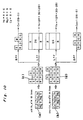
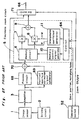
- Fig. 16 is a block diagram of an image pickup apparatus showing a first embodiment of the fourth apparatus of the present invention.
- reference numeral 1 denotes a solid state image sensor
- 2 denotes a driving circuit for the solid state image sensor 1
- 51 denotes a scan method switching circuit 51 for changing over the scan method of the solid state image sensor 1, which is controlled by the electronic zoom on/off control signal from the operation switch 52.
- the operation switch 52 gives instructions for on/off control of the electronic zoom as well as the zoom multiplying factor and screen position to be zoomed (zoom position) for on-control of the electronic zoom.
- Numeral 3 denotes an amplifier for amplifying an output signal from the solid state image sensor 1, and 4 denotes a process (signal processing) circuit for generating luminance signals and others form output of the amplifier 3.
- Numeral 5 denotes an electronic zoom circuit for enlargement-processing an output signal from the process circuit 4 through horizontal line interpolation, the electronic zoom circuit 5 generally comprising: a memory circuit 6; a memory control signal generator 10 for generating control signals for write, read, and addresses of the memory circuit 6; multipliers 7, 8 for multiplying signals of two lines read from the memory circuit 6 by their respective interpolation weight coefficients w, (1-w); a first adder 9 for adding up output signals of the multipliers 7, 8 to yield interpolation output; and an interpolation coefficient generator 11 for generating the interpolation weight coefficients w, (1-w) for signals of two lines in compliance with instructions from a control section 64.
- the control section 64 generates control signals to the memory control signal generator 10 and the interpolation coefficient generator 11 according to the zoom multiplying factor of the electronic zoom and the screen position to be zoomed (zoom position).
- Numeral 65 denotes a selector for switching between electronically zoomed output of the electronic zoom circuit 5 and non-zoomed output of the process circuit 4 in accordance with instructions from the operation switch 52, which selector feeds a signal to a vertical aperture correction circuit 13.
- Numeral 13 denotes a vertical aperture correction circuit for performing vertical aperture correction of an output image signal of the selector 65, the output of the circuit being fed to an output terminal 66.
- the vertical aperture correction circuit 13 comprises: a vertical aperture correction signal generator 15 for generating a vertical aperture correction signal out of a signal from the selector 65; a control signal generator 17 for generating a control signal k according to the interpolation coefficient w of the electronic zoom circuit 5; a third multiplier 16 for controlling the level of a vertical aperture correction signal according to the control signal k; a process circuit 14 for performing delay processing and the like to a signal from the selector 65; and a second adder 18 for adding up a signal from the process circuit 14 and that from the third multiplier 16 thereby to obtain an image signal having been controlled for the level of vertical aperture correction according to the interpolation coefficient w of the electronic zoom circuit 5.
- the selector 65 selects a signal from the process circuit 4 to feed a non-zoomed signal to the vertical aperture correction circuit 13 according to the control signal, while the control signal is led also to the scan method switching circuit 51, controlling so as to scan the solid state image sensor 1 by the same method as in the prior art shown in Fig. 32 (a first scan method).
- the signal fed to the output terminal 66 is two-field signals in interlace relation.
- the electronic zoom off control signal is led also to the electronic zoom circuit 5 thereby to stop the operation of the electronic zoom circuit 5, there are produced effects in power saving or the like.
- the selector 65 selects a signal from the electronic zoom circuit 5 to feed an electronically zoomed signal to the output terminal according to the control signal, while the control signal is led also to the scan method switching circuit 51, controlling so as to scan the solid state image sensor 1 by the method as shown in Fig. 12.
- This scan method is one in which signal charges of pixels of the solid state image sensor are scanned in such a way that the same pair of adjoining two horizontal pixel rows are scanned by one-time horizontal scan for both the odd and even fields, as shown in Fig. 12 (a second scan method). Accordingly, the two-field signals, an output signal of the solid state image sensor 1 are located at an identical position, as shown in Fig. 13 (a).
- the scan lines n, (n+1), (n+2), ... represent scan lines of the odd field, while the scan lines n', (n+1)', (n+2)', ... represent scan lines of the even field.
- the electronic zoom circuit 5 performs the electronic zoom operation as described below.
- the following description is based on the assumption that the solid state image sensor 1 outputs an image of 240 lines for one field, and therefore that of 480 lines for one frame, and that, out of these, a portion corresponding to 200 lines for one field is enlarged so as to obtain a normal one-field image, i.e. a signal of 240 lines.
- the electronic zoom circuit 5 in Fig. 16 performs interpolation processing as shown in Fig. 13 (a). That is, for the odd field, odd field output lines are obtained from odd field input lines in the same manner as in the prior art. For example, to obtain the (N+2) th line in the odd field, the (n+1) th and (n+2) th lines are read from the memory circuit 6, the readouts being multiplied by interpolation weight coefficients relative to distances (in this case, 4/12 and 8/12) and further added together. Likewise those for other output lines can be obtained by multiplying readouts of upper and lower two lines by interpolation weight coefficients relative to distances and further adding together.
- even field output lines are obtained from even field input lines in Fig. 13 (a) (the same as input of the odd field) through the same interpolation processing, where the processing is carried out so that lines obtained by the interpolation processing are in interlace relation with signals of the odd field, that is, fall just in the intermediate point between adjoining two lines of the odd field.
- the (n+1)' th and (n+2)' th input lines are read from the memory circuit 6 and the readouts are multiplied by the interpolation weight coefficients (in this case, 11/12 and 1/12) relative to distances of the intermediate point between the (N+2) th line and the (N+3) th line of the odd field and further added together.
- the vertical frequency response characteristic of the output signal interpolation-processed as above is such that, as in the prior art, a line interpolated with interpolation weight coefficients of 1/2 and 1/2 results in the perfect average of input two lines, causing the vertical frequency response characteristic to be the lowest, while a line interpolated with interpolation weight coefficients of 1 and 0 allows one line of input 0 to be output as it is, causing the frequency response characteristic to be the highest, whereas the interpolation weight coefficients of adjoining lines between the odd and even fields are not equal and therefore, for example, when lines of the odd field are interpolated with the interpolation weight coefficients of approximately 1/2 and 1/2, adjoining lines of the even field are interpolated with the interpolation weight coefficients of approximately 1 and 0 (e.g.
- the positions of high and low lines in vertical frequency response are approximately reversed between the odd and even fields, with the result that the vertical frequency response of the even field becomes high at a screen position having a low vertical frequency response in the odd field, as shown in Fig. 14.
- the resulting one-frame image in which these two field screens are synthesized has better uniformity of vertical frequency response over the entire screen.
- the output signal of the selector 65 is subjected to vertical aperture correction by the vertical aperture correction circuit 13.
- the operation is as follows.
- the control signal generator 17 forms a control signal k that depends on the interpolation weight coefficient w from the interpolation coefficient generator 11 (the signal takes a value proportional to the coefficient w when the w is less than 0.5 and proportional to that of (1-w) when the w is more than 0.5, as shown in Fig. 2), and then a vertical aperture correction signal generated by the vertical aperture correction signal generator 15 is multiplied by the control signal k by the multiplier 16, thus controlling the level of the vertical aperture correction signal. Subsequently, output of the multiplier 16 is added to a signal of the process circuit 14 (signal not subjected to vertical aperture correction) by the adder 18, so that a signal adaptively controlled in vertical sharpness according to the interpolation weight coefficient w is output.
- lines having smaller coefficients of either of the interpolation weight coefficient w or (1-w), whichever smaller, that is, those having greater vertical frequency responses as described in the section for the prior art are controlled so as to lower the level of vertical aperture correction signals
- lines having greater coefficients of either of the interpolation weight coefficient w or (1-w), whichever smaller, that is, those having smaller vertical frequency responses as described in the section for the prior art are controlled so as to heighten the level of vertical aperture correction signals. Accordingly, differences in vertical frequency response between lines of an image signal after being electronically zoomed are substantially reduced as shown in the characteristic view of Fig.
- Fig. 3 is a chart showing the vertical responses of lines of an image, similar to that shown in Fig. 30 (b).
- dotted curve represents the characteristic resulting when vertical aperture adaptive control is not performed
- solid curve represents the characteristic resulting when the level of vertical aperture correction is adaptively controlled by the vertical aperture correction circuit 13 of the present invention in Fig. 16 (controlled according to the interpolation weight coefficient w).
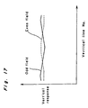
- the electronically zoomed output signal obtained at the output terminal 66 is one in which the characteristic of Fig. 13 (b) and that of Fig. 3 are combined together, resulting in the characteristic as shown in Fig. 17. That is, the vertical frequency response of the even field becomes high at a screen position having a low vertical frequency response in the odd field, and the resulting one-frame image in which these two field screens are synthesized has better uniformity of vertical frequency response over the entire screen. Moreover, differences in vertical frequency response between lines are substantially reduced in each field by the adaptive control of vertical aperture characteristic, thus eliminating the disadvantage of the prior art that the vertical frequency response of an image increases with vertical positions of the screen, resulting in a desirable image.
- the vertical aperture correction circuit 13 such one may be arranged as shown in Fig. 4, as in the description for the first and second apparatus of the present invention.
- the vertical aperture correction circuit 13 when the vertical aperture correction circuit 13 is disposed behind the electronic zoom circuit 5 that enlargement-processes an input signal through horizontal line interpolation, there are some advantages: that is, the vertical aperture correction can be effected at a stage at which the number of horizontal lines has been increased by interpolation processing, allowing aperture correction to be effected at higher vertical frequencies with the result of more increased vertical sharpness; the horizontal line of a signal subject to vertical aperture correction and the interpolation weight coefficient w correspond to each other at the ratio one to one (as apparent from Fig. 13 (a), the interpolation weight coefficient w is inherent to output line Nos., not corresponding to input line Nos. at one to one), thus allowing the level of vertical aperture correction to be accurately controlled according to the interpolation weight coefficient w, as in the first and second apparatus of the present invention.
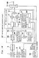
- Fig. 18 is a block diagram showing a second embodiment of the fourth apparatus of the present invention. Its difference from the first embodiment of Fig. 16 exists in that a vertical aperture correction circuit 67 is disposed ahead of the electronic zoom circuit 5, while in the embodiment of Fig. 16 the vertical aperture correction circuit 13 is disposed behind the electronic zoom circuit 5 that enlargement-processes an input signal through horizontal line interpolation.
- the same parts as in Fig. 16 are designated by the same reference numerals, and omitted in description.
- reference numeral 1 denotes a solid state image sensor
- 2 denotes a driving circuit for the solid state image sensor 1
- 3 denotes an amplifier for amplifying an output signal from the image sensor 1
- 68 denotes a process circuit for generating luminance signals and others from output of the amplifier 3
- 69 denotes a vertical aperture correction signal generator for generating a vertical aperture correction signal
- 17 denotes a control signal generator for generating a control signal k corresponding to the interpolation weight coefficient w of the electronic zoom circuit 5
- 16 denotes a third multiplier for controlling the level of a vertical aperture correction signal according to the control signal k
- 70 denotes a first adder for adding a luminance signal from the process circuit 68 and a vertical aperture correction signal from the third multiplier 16 thereby to obtain a luminance signal that has been corrected in vertical sharpness.
- Numeral 5 denotes an electronic zoom circuit for enlargement-processing an output signal from the first adder 70 by increasing the number of horizontal
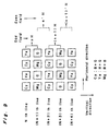
- the scan method of the solid state image sensor is switched between the aforementioned first and second scan methods depending on the on/off control of electronic zoom, the construction shown in Fig. 9 is preferable for the color filter of the solid state image sensor. In this case, the scan method is switched as shown in Fig. 19.
- Fig. 20 and Fig. 21 are block diagrams of image pickup apparatus showing a third and a fourth embodiment of the fourth apparatus of the present invention, respectively, where Fig. 20 is a variation of the first embodiment of Fig. 16, and Fig. 21 is that of the second embodiment of Fig. 18.
- the content of the variation is that while the scan method of the solid state image sensor 1 is switched only with the on/off control signal of electronic zoom in the first and second embodiments, it is instead arranged that the scan method is switched with the on/off control signal of electronic zoom and the zoom multiplying factor.
- a scan method switching circuit 67 there are led an of/off control signal of electronic zoom from the operation switch 52 and a zoom multiplying factor control signal, where, only when the electronic zoom control is on and moreover the zoom multiplying factor is over a specified value, the scan method of the solid state image sensor 1 is switched to the second scan method, so that the electronic zoom circuit 5 performs interpolation processing according to the scan method.
- the remaining construction and operation are the same as in the first embodiment of Fig. 16 and the second embodiment of Fig. 18, thus omitted in description.
- the fourth apparatus of the present invention has been described as above using a primary interpolation as the horizontal line interpolation method (a method that the mid-point line is obtained out of two adjoining lines, the Sn th and (Sn+1) th line by a calculation of wSn + (1 - w) Sn + 1)
- the interpolation method is not necessarily limited thereto and the present invention can apparently be achieved by any such method if the level of vertical aperture correction is controlled with interpolation weight coefficients according to the method.
- the fifth and sixth apparatus are described below with reference to the accompanying drawings, taking the case of an image pickup apparatus with electronic zoom function provided with image enlargement function as an image enlarging apparatus.
- Fig. 22 is a block diagram of an image pickup apparatus with electronic zoom function showing a first embodiment of the fifth and sixth apparatus of the present invention.
- reference numeral 1 denotes an image sensor
- 2 denotes a driving circuit for the image sensor 1
- 72 denotes a gain control amplifier for amplifying an output signal from the image sensor 1
- 73 denotes a gain control signal generator for generating a control signal to control the gain of the gain control amplifier 72
- 4 denotes a process circuit for generating luminance signals and others from output of the gain control amplifier 72.
- Numeral 5 denotes an electronic zoom circuit for enlargement-processing an output signal from the process circuit 4, the electronic zoom circuit generally comprising: a memory circuit 6; a memory control signal generator 10 for generating control signals for write, read, and addresses of the memory circuit 6; multipliers 7, 8 for multiplying signals of two lines read from the memory circuit 6 by their respective interpolation weight coefficients w, (1-w); an adder 9 for adding up output signals of the multipliers 7, 8 to yield interpolation output; and an interpolation coefficient generator 11 for generating the interpolation weight coefficients w, (1-w) for signals of two lines in accordance with instructions from a control section 12.
- the control section 12 controls the zoom multiplying factor of the electronic zoom and the screen position to be zoomed (zoom position).
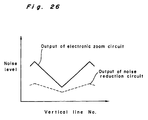
- Numeral 74 denotes a noise reduction circuit for reducing noise of an output image signal of the electronic zoom circuit 5, the output of the noise reduction circuit 74 being fed to an output terminal 76.
- the noise reduction circuit 74 is controlled for its reduction characteristic by a control signal C from a noise reduction control signal generator 75, where the noise reduction control signal generator 75 forms a control signal C from the interpolation weight coefficients w, (1-w) derived from the interpolation coefficient generator 11.
- the noise reduction control signal generator 75 forms a control signal C corresponding to either of the interpolation weight coefficients w, (1-w) from the interpolation coefficient generator circuit 11, whichever smaller (resulting in a smaller value of the signal for a smaller coefficient, a greater value for greater coefficient).
- the control signal C is a smaller one
- the noise reduction circuit 74 is controlled so as to give a greater amount of noise reduction
- the control signal C is a greater one
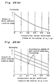
- it is controlled so as to give a smaller amount of noise reduction. Accordingly, the noise reduction characteristic depending on the smaller of the interpolation weight coefficients w and (1-w) results in such one as shown in Fig. 25 (a).
- Fig. 26 is a chart showing the noise level characteristic of each line, similar to that of Fig. 35 (c), where solid line represents the output (i.e.
- the above-described first embodiment is arranged so that the noise reduction characteristic of the noise reduction circuit 74 is controlled depending on the interpolation weight coefficient w, (1-w) from the interpolation coefficient generator 11, it may otherwise be arranged so as to make all the lines uniformly subjected to noise reduction, in which the S/N ratio over the entire screen is also improved such as to suppress the afore-noted disturbing lateral stripes due to noise differences between lines.
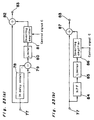
- Fig. 23 (a) shows a so-called line noise cancel circuit, which serves to reduce noise depending on the fact that an image signal has a great correlation between lines.
- the noise cancel circuit extracts approximately only noise components out of a zoom-processed image signal entered into an input terminal 77 by a 1 horizontal-scan-period delay circuit 78 (hereinafter, referred to as 1H delay circuit), a subtracter circuit 79 and a limiter 80, the resulting output being amplified by an inverting amplifier 81 and added to the input image signal by an adder circuit 82, thus feeding the noise-reduced output to an output terminal 83.
- amplification degree of the inverting amplifier 81 is controlled by the control signal C from the noise reduction control signal generator 75, thus controlling the noise reduction characteristic depending on the interpolation characteristic of electronic zoom.
- Fig. 23 (b) shows another example of the noise reduction circuit, which reduces noise depending on the fact that noise of an image signal is concentrated in high-frequency range.
- the circuit extracts high-frequency components containing more noise components out of a zoom-processed image signal entered into the input terminal 77 by a high-pass filter (HPF) 84, and the high-frequency components are made to pass through a limiter circuit 85, thus extracting approximate only noise components.
- the output is amplified by an inverting amplifier 86 and added to the input image signal by an adder circuit 87, thus feeding a noise-reduced output to the output terminal 83.
- amplification degree of the inverting amplifier 86 is controlled by the control signal C from the noise reduction control signal generator 75, controlling the noise reduction characteristic depending on the interpolation characteristic of electronic zoom.
- noise reduction circuit is arranged so that noise reduction characteristic is controlled depending on interpolation characteristic of electronic zoom by controlling the degree of amplification of the inverting amplifiers 81, 86 with the control signal C from the noise reduction control signal generator 75, it is also possible as another embodiment that noise reduction characteristic is controlled depending on interpolation characteristic of electronic zoom by controlling the limiter characteristic of the limiter circuits 80, 85 with the control signal C from the noise reduction control signal generator circuit 75.
- Fig. 24 is a block diagram of an image pickup apparatus with electronic zoom function showing a second embodiment of the fifth apparatus of the present invention. Its difference from the first embodiment of Fig. 22 exists in that while in the first embodiment noise reduction characteristic of the noise reduction circuit 74 is controlled only by the interpolation weight coefficient w, (1-w) from the interpolation coefficient generator 11, the noise reduction characteristic of the noise reduction circuit 74 is instead controlled depending on both the interpolation weight coefficient w, (1-w) from the interpolation coefficient generator 11 and the amplification degree of the gain control amplifier 72.
- a noise reduction control signal generator 88 forms a control signal C corresponding to both a signal for controlling the amplification degree of the gain control amplifier 72 from the gain control signal generator 73 and either of the interpolation weight coefficients w, (1-w) from the interpolation coefficient generator 11, whichever smaller.
- the noise reduction characteristic is controlled depending on both the interpolation weight coefficients w, (1-w) and the amplification degree of the gain control amplifier 72, similar effect can be obtained also when the noise reduction characteristic of the noise reduction circuit 74 is controlled depending on only the amplification degree of the gain control amplifier 72.
- the present invention can generally be applied to image enlargement apparatus which electronically enlarge images without limiting to image pickup apparatus such as described above.
- the image sensor 1 and the driving circuit 2 in Fig. 22 and Fig. 24 are omitted and the gain control amplifier 72 has direct input of an image signal led thereto, and that the process circuit 4 may also be omitted if unnecessary.
- any electronic zoom circuit may be incorporated in the construction of the present invention without limiting to the electronic zoom circuits such as described above.
Landscapes
- Engineering & Computer Science (AREA)
- Physics & Mathematics (AREA)
- Multimedia (AREA)
- Signal Processing (AREA)
- General Physics & Mathematics (AREA)
- Theoretical Computer Science (AREA)
- Data Mining & Analysis (AREA)
- Computational Mathematics (AREA)
- Mathematical Analysis (AREA)
- Mathematical Optimization (AREA)
- Pure & Applied Mathematics (AREA)
- Mathematical Physics (AREA)
- Algebra (AREA)
- Databases & Information Systems (AREA)
- Software Systems (AREA)
- General Engineering & Computer Science (AREA)
- Spectroscopy & Molecular Physics (AREA)
- Transforming Light Signals Into Electric Signals (AREA)
- Studio Devices (AREA)
Claims (4)
- Procédé d'interpolation de lignes horizontales destiné à modifier le nombre des lignes horizontales, comprenant les étapes consistant à :générer des coefficients d'interpolation destinés à exécuter un traitement d'interpolation pour des lignes horizontales d'un signal d'image d'entrée,obtenir un signal d'image de sortie étendu dans une direction verticale en exécutant le traitement d'interpolation pour les lignes horizontales du signal d'image d'entrée suivant les coefficients d'interpolation,générer un signal de netteté verticale sur la base du signal d'image d'entrée ou du signal d'image de sortie,commander un gain du signal de netteté verticale suivant les coefficients d'interpolation et ajouter ensuite le signal de netteté verticale commandé au signal d'image d'entrée, au signal d'image de sortie, à un signal obtenu par le traitement du signal d'image d'entrée ou à un signal obtenu par le traitement du signal d'image de sortie.
- Circuit d'interpolation de lignes horizontales destiné à modifier le nombre des lignes horizontales, comprenant :un circuit de génération de coefficients d'interpolation (11) destiné à générer des coefficients d'interpolation en vue d'exécuter un traitement d'interpolation pour des lignes horizontales d'un signal d'image d'entrée,un circuit d'interpolation de lignes (7, 8, 9) destiné à obtenir un signal d'image de sortie étendu dans une direction verticale en exécutant le traitement d'interpolation pour les lignes horizontales du signal d'image d'entrée suivant les coefficients d'interpolation,un circuit de génération de signal de netteté verticale (15, 69) destiné à générer un signal de netteté verticale sur la base du signal d'image d'entrée ou du signal d'image de sortie,un amplificateur à gain commandable (16, 17) destiné à commander un gain du signal de netteté verticale suivant les coefficients d'interpolation, etun additionneur (18, 35, 70) destiné à additionner un signal de sortie généré depuis l'amplificateur à gain commandable au signal d'image d'entrée, au signal d'image de sortie, ou à un signal obtenu en traitant le signal d'image d'entrée ou à un signal obtenu en traitant le signal d'image de sortie.
- Circuit d'interpolation de lignes horizontales selon la revendication 2,
dans lequel le circuit de génération de signal de netteté verticale (15) génère le signal de netteté verticale sur la base du signal d'image de sortie du circuit d'interpolation de lignes, et
l'additionneur (18) additionne le signal de sortie généré à partir de l'amplificateur à gain commandable au signal d'image de sortie ou au signal obtenu en traitant le signal d'image de sortie. - Circuit d'interpolation de lignes horizontales selon la revendication 2,
dans lequel le circuit de génération de signal de netteté verticale (15) génère le signal de netteté verticale sur la base du signal d'image d'entrée,
l'additionneur (35) additionne le signal de sortie généré à partir de l'amplificateur à gain commandable au signal d'image d'entrée ou au signal obtenu en traitant le signal d'image d'entrée.
Applications Claiming Priority (12)
| Application Number | Priority Date | Filing Date | Title |
|---|---|---|---|
| JP25800390 | 1990-09-26 | ||
| JP258003/90 | 1990-09-26 | ||
| JP2258002A JPH04134979A (ja) | 1990-09-26 | 1990-09-26 | 撮像装置 |
| JP258002/90 | 1990-09-26 | ||
| JP2258003A JP2890774B2 (ja) | 1990-09-26 | 1990-09-26 | 画像拡大装置と電子ズーム機能付き撮像装置 |
| JP25800290 | 1990-09-26 | ||
| JP2285004A JP2858372B2 (ja) | 1990-10-22 | 1990-10-22 | 水平ライン補間回路および撮像装置 |
| JP285004/90 | 1990-10-22 | ||
| JP28500490 | 1990-10-22 | ||
| JP3064476A JPH04299678A (ja) | 1991-03-28 | 1991-03-28 | 撮像装置 |
| JP64476/91 | 1991-03-28 | ||
| JP6447691 | 1991-03-28 |
Publications (3)
| Publication Number | Publication Date |
|---|---|
| EP0477884A2 EP0477884A2 (fr) | 1992-04-01 |
| EP0477884A3 EP0477884A3 (en) | 1994-06-08 |
| EP0477884B1 true EP0477884B1 (fr) | 2002-06-05 |
Family
ID=27464441
Family Applications (1)
| Application Number | Title | Priority Date | Filing Date |
|---|---|---|---|
| EP91116300A Expired - Lifetime EP0477884B1 (fr) | 1990-09-26 | 1991-09-25 | Circuit pour l'interpolation de lignes horizontales et dispositifs de prise d'image le comportant |
Country Status (3)
| Country | Link |
|---|---|
| US (3) | US5268758A (fr) |
| EP (1) | EP0477884B1 (fr) |
| DE (1) | DE69133027T2 (fr) |
Families Citing this family (36)
| Publication number | Priority date | Publication date | Assignee | Title |
|---|---|---|---|---|
| US6278803B1 (en) * | 1990-04-26 | 2001-08-21 | Canon Kabushiki Kaisha | Interpolation apparatus for offset sampling signals |
| WO1994003015A1 (fr) * | 1992-07-22 | 1994-02-03 | Matsushita Electric Industrial Co., Ltd. | Dispositif d'imagerie a fonction d'interpolation des lignes horizontales |
| JP3196354B2 (ja) * | 1992-10-13 | 2001-08-06 | 株式会社日立製作所 | 輪郭補正回路及び撮像装置 |
| JPH06133206A (ja) * | 1992-10-19 | 1994-05-13 | Canon Inc | 撮像装置のオートフォーカス方式 |
| US6236431B1 (en) * | 1993-05-27 | 2001-05-22 | Canon Kabushiki Kaisha | Video camera apparatus with distance measurement area adjusted based on electronic magnification |
| DE69433374T2 (de) * | 1993-09-17 | 2004-10-07 | Canon Kk | Bildaufnahmegerät |
| JP3336544B2 (ja) * | 1994-04-25 | 2002-10-21 | 富士写真フイルム株式会社 | デジタル画像処理装置 |
| GB9410784D0 (en) * | 1994-05-28 | 1994-07-20 | Kodak Ltd | Image processing |
| CN1136381A (zh) * | 1994-08-31 | 1996-11-20 | 索尼公司 | 摄象装置 |
| JP3581443B2 (ja) * | 1995-07-11 | 2004-10-27 | キヤノン株式会社 | 画像処理装置及びその方法 |
| FR2737324B1 (fr) * | 1995-07-26 | 1997-09-26 | Winbond Electronics Corp | Procede et dispositif pour changer l'echelle d'une image numerique de facon uniforme |
| JPH09101765A (ja) * | 1995-07-31 | 1997-04-15 | Canon Inc | 画像処理装置 |
| US5835160A (en) * | 1995-09-13 | 1998-11-10 | Oak Technology, Inc. | Sampling rate conversion using digital differential analyzers |
| US5748307A (en) * | 1996-01-05 | 1998-05-05 | Chinon Kabushiki Kaisha | Image pickup apparatus |
| JP3755921B2 (ja) * | 1996-02-29 | 2006-03-15 | 株式会社コダックデジタルプロダクトセンター | 撮像デバイスのラインノイズ除去方法及びそれを用いたラインノイズ除去装置 |
| JP3787927B2 (ja) * | 1996-11-18 | 2006-06-21 | ソニー株式会社 | 撮像装置及びカラー画像信号の処理方法 |
| MY119346A (en) | 1996-12-24 | 2005-05-31 | Sony Corp | Picture processing apparatus and method |
| US6166831A (en) * | 1997-12-15 | 2000-12-26 | Analog Devices, Inc. | Spatially offset, row interpolated image sensor |
| JPH11298862A (ja) * | 1998-04-10 | 1999-10-29 | Seiko Epson Corp | 画像処理方法及び画像表示装置 |
| EP1110381B1 (fr) * | 1998-08-28 | 2003-07-16 | Sarnoff Corporation | Procede et dispositif permettant d'ameliorer des images electroniquement |
| JP3365333B2 (ja) * | 1999-03-03 | 2003-01-08 | 日本電気株式会社 | 解像度変換装置 |
| JP3991543B2 (ja) | 2000-01-11 | 2007-10-17 | 株式会社日立製作所 | 撮像装置 |
| US6718074B1 (en) | 2000-06-02 | 2004-04-06 | Cognex Corporation | Method and apparatus for inspection for under-resolved features in digital images |
| GB0027238D0 (en) * | 2000-11-08 | 2000-12-27 | Secr Defence | Adaptive filter |
| WO2002063543A2 (fr) | 2001-01-22 | 2002-08-15 | Hand Held Products, Inc. | Lecteur optique presentant un mode de fonctionnement a trame partielle |
| US7268924B2 (en) | 2001-01-22 | 2007-09-11 | Hand Held Products, Inc. | Optical reader having reduced parameter determination delay |
| JP2004159067A (ja) * | 2002-11-06 | 2004-06-03 | Sanyo Electric Co Ltd | 垂直シャープネス装置及びそれを備えたtv受像機 |
| JP4178455B2 (ja) * | 2003-01-21 | 2008-11-12 | ソニー株式会社 | フレーム変換方法、フレーム変換回路および電子カメラ |
| US7750945B2 (en) | 2004-10-13 | 2010-07-06 | Panasonic Corporation | Video signal processing device and image processing device |
| US7697049B1 (en) * | 2005-05-04 | 2010-04-13 | Samsung Electrics Co., Ltd. | Better SNR ratio for downsized images using interlaced mode |
| US7898581B2 (en) * | 2006-05-08 | 2011-03-01 | Panasonic Corporation | Image pickup apparatus with noise reduction unit |
| US7956907B2 (en) * | 2006-08-23 | 2011-06-07 | Panasonic Corporation | Image capture device with low-frequency noise suppression |
| EP2019424B1 (fr) | 2007-07-26 | 2016-11-23 | SEMIKRON Elektronik GmbH & Co. KG | Module semi-conducteur de puissance doté d'un dispositif étanche destiné au support de substrat et son procédé de fabrication |
| TWI413101B (zh) * | 2009-08-13 | 2013-10-21 | Novatek Microelectronics Corp | 增進亮度一致性的控制方法及相關亮度校正控制器與顯示裝置 |
| US20110298972A1 (en) | 2010-06-04 | 2011-12-08 | Stmicroelectronics Asia Pacific Pte. Ltd. | System and process for image rescaling using adaptive interpolation kernel with sharpness and de-ringing control |
| KR102295526B1 (ko) | 2017-04-10 | 2021-08-30 | 삼성전자 주식회사 | 이미지 센서 및 이를 포함하는 이미지 처리 장치 |
Family Cites Families (20)
| Publication number | Priority date | Publication date | Assignee | Title |
|---|---|---|---|---|
| GB1594341A (en) * | 1976-10-14 | 1981-07-30 | Micro Consultants Ltd | Picture information processing system for television |
| NL7709662A (nl) * | 1977-09-02 | 1979-03-06 | Philips Nv | Televisiekamera. |
| JPS56119909A (en) * | 1980-02-22 | 1981-09-19 | Victor Co Of Japan Ltd | Reproducing device for speed variable digital signal |
| GB2140644B (en) * | 1983-05-17 | 1986-09-17 | Sony Corp | Television standards converters |
| US5083204A (en) * | 1984-10-01 | 1992-01-21 | Hughes Aircraft Company | Signal processor for an imaging sensor system |
| EP0179594A1 (fr) * | 1984-10-23 | 1986-04-30 | EMI Limited | Traitement de signaux d'image |
| US4746985A (en) * | 1985-04-11 | 1988-05-24 | Rank Cintel Limited | Generating picture effects in video signals |
| GB2183118B (en) * | 1985-11-19 | 1989-10-04 | Sony Corp | Image signal processing |
| JPS63290014A (ja) * | 1987-05-22 | 1988-11-28 | Nippon Hoso Kyokai <Nhk> | ディジタル振幅変調器 |
| JPS6481472A (en) * | 1987-09-24 | 1989-03-27 | Hitachi Electronics | Television camera device |
| JPH01170280A (ja) * | 1987-12-25 | 1989-07-05 | Matsushita Electric Ind Co Ltd | 固体撮像装置 |
| JP2551629B2 (ja) * | 1988-06-21 | 1996-11-06 | 株式会社日立製作所 | 撮像装置 |
| JPH0229178A (ja) * | 1988-07-19 | 1990-01-31 | Sony Corp | 映像信号処理回路 |
| JPH02111188A (ja) * | 1988-10-20 | 1990-04-24 | Toshiba Corp | 画質改善装置 |
| US4988984A (en) * | 1988-10-31 | 1991-01-29 | International Business Machines Corporation | Image interpolator for an image display system |
| US4962419A (en) * | 1989-02-13 | 1990-10-09 | Eastman Kodak Company | Detail processing method and apparatus providing uniform processing of horizontal and vertical detail components |
| JP2621469B2 (ja) * | 1989-03-23 | 1997-06-18 | 松下電器産業株式会社 | ビデオカメラ装置 |
| JPH031669A (ja) * | 1989-05-29 | 1991-01-08 | Canon Inc | 動画/静止画変換装置 |
| KR920005018B1 (ko) * | 1989-07-20 | 1992-06-22 | 삼성전자 주식회사 | 텔레비젼수상기에 있어서 동작적응형 수직윤곽 보상회로 |
| JP2533393B2 (ja) * | 1990-02-16 | 1996-09-11 | シャープ株式会社 | Ntsc―hdコンバ―タ |
-
1991
- 1991-09-24 US US07/765,036 patent/US5268758A/en not_active Expired - Lifetime
- 1991-09-25 EP EP91116300A patent/EP0477884B1/fr not_active Expired - Lifetime
- 1991-09-25 DE DE69133027T patent/DE69133027T2/de not_active Expired - Fee Related
-
1993
- 1993-08-12 US US08/104,913 patent/US5517239A/en not_active Expired - Lifetime
-
1995
- 1995-06-01 US US08/456,406 patent/US5521636A/en not_active Expired - Lifetime
Also Published As
| Publication number | Publication date |
|---|---|
| DE69133027T2 (de) | 2003-01-30 |
| EP0477884A2 (fr) | 1992-04-01 |
| EP0477884A3 (en) | 1994-06-08 |
| DE69133027D1 (de) | 2002-07-11 |
| US5268758A (en) | 1993-12-07 |
| US5521636A (en) | 1996-05-28 |
| US5517239A (en) | 1996-05-14 |
Similar Documents
| Publication | Publication Date | Title |
|---|---|---|
| EP0477884B1 (fr) | Circuit pour l'interpolation de lignes horizontales et dispositifs de prise d'image le comportant | |
| JP3242515B2 (ja) | 撮像装置 | |
| JP3074967B2 (ja) | 高ダイナミックレンジ撮像・合成方法及び高ダイナミックレンジ撮像装置 | |
| US6693676B2 (en) | Motion detecting apparatus for detecting motion information of picture within signal | |
| JP4372955B2 (ja) | 固体撮像装置および信号処理方法 | |
| JPH0335870B2 (fr) | ||
| KR920001009B1 (ko) | 촬상장치 | |
| JPH0636602B2 (ja) | 雑音低減回路 | |
| EP0461615B1 (fr) | Appareil de prise de vues en couleurs | |
| JPH1175118A (ja) | ビデオカメラ | |
| US6690418B1 (en) | Image sensing apparatus image signal controller and method | |
| US7265785B2 (en) | Imaging apparatus and method that provide high resolution under low illumination without substantial S/N degradation | |
| JPH0884348A (ja) | 撮像装置 | |
| JP2001086394A (ja) | 撮像装置 | |
| US5912702A (en) | Video camera and image enhancing apparatus | |
| JP3578246B2 (ja) | 固体撮像装置 | |
| JP3992403B2 (ja) | 画像信号処理装置および画像信号処理方法 | |
| JPH0662325A (ja) | 固体撮像素子を使用した撮像装置 | |
| JP2511968B2 (ja) | 撮像装置 | |
| JP2698404B2 (ja) | 輝度信号処理装置 | |
| JP2010193112A (ja) | 画像処理装置およびディジタルスチルカメラ | |
| JP3524211B2 (ja) | 撮像装置 | |
| JP4033641B2 (ja) | 固体撮像装置 | |
| JPH11239294A (ja) | ビデオカメラ | |
| KR0141107B1 (ko) | 비월주사신호의 순차주사신호로의 변환회로 |
Legal Events
| Date | Code | Title | Description |
|---|---|---|---|
| PUAI | Public reference made under article 153(3) epc to a published international application that has entered the european phase |
Free format text: ORIGINAL CODE: 0009012 |
|
| 17P | Request for examination filed |
Effective date: 19910925 |
|
| AK | Designated contracting states |
Kind code of ref document: A2 Designated state(s): DE FR GB |
|
| PUAL | Search report despatched |
Free format text: ORIGINAL CODE: 0009013 |
|
| AK | Designated contracting states |
Kind code of ref document: A3 Designated state(s): DE FR GB |
|
| 17Q | First examination report despatched |
Effective date: 19990318 |
|
| RIC1 | Information provided on ipc code assigned before grant |
Free format text: 7G 06T 3/40 A, 7G 06F 17/17 B |
|
| GRAG | Despatch of communication of intention to grant |
Free format text: ORIGINAL CODE: EPIDOS AGRA |
|
| GRAG | Despatch of communication of intention to grant |
Free format text: ORIGINAL CODE: EPIDOS AGRA |
|
| GRAH | Despatch of communication of intention to grant a patent |
Free format text: ORIGINAL CODE: EPIDOS IGRA |
|
| GRAH | Despatch of communication of intention to grant a patent |
Free format text: ORIGINAL CODE: EPIDOS IGRA |
|
| GRAA | (expected) grant |
Free format text: ORIGINAL CODE: 0009210 |
|
| AK | Designated contracting states |
Kind code of ref document: B1 Designated state(s): DE FR GB |
|
| REG | Reference to a national code |
Ref country code: GB Ref legal event code: FG4D |
|
| REF | Corresponds to: |
Ref document number: 69133027 Country of ref document: DE Date of ref document: 20020711 |
|
| ET | Fr: translation filed | ||
| PLBE | No opposition filed within time limit |
Free format text: ORIGINAL CODE: 0009261 |
|
| STAA | Information on the status of an ep patent application or granted ep patent |
Free format text: STATUS: NO OPPOSITION FILED WITHIN TIME LIMIT |
|
| 26N | No opposition filed |
Effective date: 20030306 |
|
| PGFP | Annual fee paid to national office [announced via postgrant information from national office to epo] |
Ref country code: FR Payment date: 20080915 Year of fee payment: 18 |
|
| PGFP | Annual fee paid to national office [announced via postgrant information from national office to epo] |
Ref country code: DE Payment date: 20081002 Year of fee payment: 18 |
|
| PGFP | Annual fee paid to national office [announced via postgrant information from national office to epo] |
Ref country code: GB Payment date: 20081001 Year of fee payment: 18 |
|
| GBPC | Gb: european patent ceased through non-payment of renewal fee |
Effective date: 20090925 |
|
| REG | Reference to a national code |
Ref country code: FR Ref legal event code: ST Effective date: 20100531 |
|
| PG25 | Lapsed in a contracting state [announced via postgrant information from national office to epo] |
Ref country code: DE Free format text: LAPSE BECAUSE OF NON-PAYMENT OF DUE FEES Effective date: 20100401 Ref country code: FR Free format text: LAPSE BECAUSE OF NON-PAYMENT OF DUE FEES Effective date: 20090930 |
|
| PG25 | Lapsed in a contracting state [announced via postgrant information from national office to epo] |
Ref country code: GB Free format text: LAPSE BECAUSE OF NON-PAYMENT OF DUE FEES Effective date: 20090925 |