EP0476661B1 - Dispositif semi-conducteur du type à contact par pression - Google Patents
Dispositif semi-conducteur du type à contact par pression Download PDFInfo
- Publication number
- EP0476661B1 EP0476661B1 EP19910115961 EP91115961A EP0476661B1 EP 0476661 B1 EP0476661 B1 EP 0476661B1 EP 19910115961 EP19910115961 EP 19910115961 EP 91115961 A EP91115961 A EP 91115961A EP 0476661 B1 EP0476661 B1 EP 0476661B1
- Authority
- EP
- European Patent Office
- Prior art keywords
- electrode
- pellet
- soft
- semiconductor device
- metal plate
- Prior art date
- Legal status (The legal status is an assumption and is not a legal conclusion. Google has not performed a legal analysis and makes no representation as to the accuracy of the status listed.)
- Expired - Lifetime
Links
Images


Classifications
-
- H—ELECTRICITY
- H01—ELECTRIC ELEMENTS
- H01L—SEMICONDUCTOR DEVICES NOT COVERED BY CLASS H10
- H01L24/00—Arrangements for connecting or disconnecting semiconductor or solid-state bodies; Methods or apparatus related thereto
- H01L24/71—Means for bonding not being attached to, or not being formed on, the surface to be connected
- H01L24/72—Detachable connecting means consisting of mechanical auxiliary parts connecting the device, e.g. pressure contacts using springs or clips
-
- H—ELECTRICITY
- H01—ELECTRIC ELEMENTS
- H01L—SEMICONDUCTOR DEVICES NOT COVERED BY CLASS H10
- H01L23/00—Details of semiconductor or other solid state devices
- H01L23/02—Containers; Seals
- H01L23/04—Containers; Seals characterised by the shape of the container or parts, e.g. caps, walls
- H01L23/043—Containers; Seals characterised by the shape of the container or parts, e.g. caps, walls the container being a hollow construction and having a conductive base as a mounting as well as a lead for the semiconductor body
- H01L23/051—Containers; Seals characterised by the shape of the container or parts, e.g. caps, walls the container being a hollow construction and having a conductive base as a mounting as well as a lead for the semiconductor body another lead being formed by a cover plate parallel to the base plate, e.g. sandwich type
-
- H—ELECTRICITY
- H01—ELECTRIC ELEMENTS
- H01L—SEMICONDUCTOR DEVICES NOT COVERED BY CLASS H10
- H01L2224/00—Indexing scheme for arrangements for connecting or disconnecting semiconductor or solid-state bodies and methods related thereto as covered by H01L24/00
- H01L2224/01—Means for bonding being attached to, or being formed on, the surface to be connected, e.g. chip-to-package, die-attach, "first-level" interconnects; Manufacturing methods related thereto
- H01L2224/26—Layer connectors, e.g. plate connectors, solder or adhesive layers; Manufacturing methods related thereto
- H01L2224/2612—Auxiliary members for layer connectors, e.g. spacers
-
- H—ELECTRICITY
- H01—ELECTRIC ELEMENTS
- H01L—SEMICONDUCTOR DEVICES NOT COVERED BY CLASS H10
- H01L2924/00—Indexing scheme for arrangements or methods for connecting or disconnecting semiconductor or solid-state bodies as covered by H01L24/00
- H01L2924/01—Chemical elements
- H01L2924/01004—Beryllium [Be]
-
- H—ELECTRICITY
- H01—ELECTRIC ELEMENTS
- H01L—SEMICONDUCTOR DEVICES NOT COVERED BY CLASS H10
- H01L2924/00—Indexing scheme for arrangements or methods for connecting or disconnecting semiconductor or solid-state bodies as covered by H01L24/00
- H01L2924/01—Chemical elements
- H01L2924/01005—Boron [B]
-
- H—ELECTRICITY
- H01—ELECTRIC ELEMENTS
- H01L—SEMICONDUCTOR DEVICES NOT COVERED BY CLASS H10
- H01L2924/00—Indexing scheme for arrangements or methods for connecting or disconnecting semiconductor or solid-state bodies as covered by H01L24/00
- H01L2924/01—Chemical elements
- H01L2924/01006—Carbon [C]
-
- H—ELECTRICITY
- H01—ELECTRIC ELEMENTS
- H01L—SEMICONDUCTOR DEVICES NOT COVERED BY CLASS H10
- H01L2924/00—Indexing scheme for arrangements or methods for connecting or disconnecting semiconductor or solid-state bodies as covered by H01L24/00
- H01L2924/01—Chemical elements
- H01L2924/01013—Aluminum [Al]
-
- H—ELECTRICITY
- H01—ELECTRIC ELEMENTS
- H01L—SEMICONDUCTOR DEVICES NOT COVERED BY CLASS H10
- H01L2924/00—Indexing scheme for arrangements or methods for connecting or disconnecting semiconductor or solid-state bodies as covered by H01L24/00
- H01L2924/01—Chemical elements
- H01L2924/01015—Phosphorus [P]
-
- H—ELECTRICITY
- H01—ELECTRIC ELEMENTS
- H01L—SEMICONDUCTOR DEVICES NOT COVERED BY CLASS H10
- H01L2924/00—Indexing scheme for arrangements or methods for connecting or disconnecting semiconductor or solid-state bodies as covered by H01L24/00
- H01L2924/01—Chemical elements
- H01L2924/01029—Copper [Cu]
-
- H—ELECTRICITY
- H01—ELECTRIC ELEMENTS
- H01L—SEMICONDUCTOR DEVICES NOT COVERED BY CLASS H10
- H01L2924/00—Indexing scheme for arrangements or methods for connecting or disconnecting semiconductor or solid-state bodies as covered by H01L24/00
- H01L2924/01—Chemical elements
- H01L2924/01033—Arsenic [As]
-
- H—ELECTRICITY
- H01—ELECTRIC ELEMENTS
- H01L—SEMICONDUCTOR DEVICES NOT COVERED BY CLASS H10
- H01L2924/00—Indexing scheme for arrangements or methods for connecting or disconnecting semiconductor or solid-state bodies as covered by H01L24/00
- H01L2924/01—Chemical elements
- H01L2924/01042—Molybdenum [Mo]
-
- H—ELECTRICITY
- H01—ELECTRIC ELEMENTS
- H01L—SEMICONDUCTOR DEVICES NOT COVERED BY CLASS H10
- H01L2924/00—Indexing scheme for arrangements or methods for connecting or disconnecting semiconductor or solid-state bodies as covered by H01L24/00
- H01L2924/01—Chemical elements
- H01L2924/01078—Platinum [Pt]
-
- H—ELECTRICITY
- H01—ELECTRIC ELEMENTS
- H01L—SEMICONDUCTOR DEVICES NOT COVERED BY CLASS H10
- H01L2924/00—Indexing scheme for arrangements or methods for connecting or disconnecting semiconductor or solid-state bodies as covered by H01L24/00
- H01L2924/01—Chemical elements
- H01L2924/01079—Gold [Au]
-
- H—ELECTRICITY
- H01—ELECTRIC ELEMENTS
- H01L—SEMICONDUCTOR DEVICES NOT COVERED BY CLASS H10
- H01L2924/00—Indexing scheme for arrangements or methods for connecting or disconnecting semiconductor or solid-state bodies as covered by H01L24/00
- H01L2924/01—Chemical elements
- H01L2924/01082—Lead [Pb]
-
- H—ELECTRICITY
- H01—ELECTRIC ELEMENTS
- H01L—SEMICONDUCTOR DEVICES NOT COVERED BY CLASS H10
- H01L2924/00—Indexing scheme for arrangements or methods for connecting or disconnecting semiconductor or solid-state bodies as covered by H01L24/00
- H01L2924/01—Chemical elements
- H01L2924/01088—Radium [Ra]
-
- H—ELECTRICITY
- H01—ELECTRIC ELEMENTS
- H01L—SEMICONDUCTOR DEVICES NOT COVERED BY CLASS H10
- H01L2924/00—Indexing scheme for arrangements or methods for connecting or disconnecting semiconductor or solid-state bodies as covered by H01L24/00
- H01L2924/10—Details of semiconductor or other solid state devices to be connected
- H01L2924/11—Device type
- H01L2924/13—Discrete devices, e.g. 3 terminal devices
- H01L2924/1301—Thyristor
-
- H—ELECTRICITY
- H01—ELECTRIC ELEMENTS
- H01L—SEMICONDUCTOR DEVICES NOT COVERED BY CLASS H10
- H01L2924/00—Indexing scheme for arrangements or methods for connecting or disconnecting semiconductor or solid-state bodies as covered by H01L24/00
- H01L2924/10—Details of semiconductor or other solid state devices to be connected
- H01L2924/11—Device type
- H01L2924/13—Discrete devices, e.g. 3 terminal devices
- H01L2924/1304—Transistor
- H01L2924/1305—Bipolar Junction Transistor [BJT]
- H01L2924/13055—Insulated gate bipolar transistor [IGBT]
Definitions
- the invention relates to a press-contact type semiconductor device as disclosed in DE-A-2 556 469.
- This prior art press-contact type semiconductor device comprises a pellet having upper and lower surfaces, said pellet having a mesa portion formed on said upper surface, said lower surface being flat, and a semiconductor element being formed in said pellet; a first pellet electrode formed on the mesa portion and on the upper surface of said pellet; a second pellet electrode formed on the lower surface of said pellet; a first electrode post which is provided in said package so as to be located above said first pellet electrode, and to which pressure is applied; a second electrode post which is provided in said package so as to be located below said second pellet electrode, and to which the pressure is applied; and a soft-metal layer arranged between said first pellet electrode and said first electrode post and having projections along its surface.
- the semiconductor element is covered at the side surfaces or edges thereof by a protective layer also covering the top major surface and the bottom major surface of the semiconductor element.
- the bottom surface of the second pellet electrode comprises indentations and projections, and the entire bottom surface of the second pellet electrode is covered by a thin layer made of e.g. tin.
- the protective layer of the semiconductor element also covers the top major surface of the semiconductor element.
- the projections of the second pellet electrode with the tin layer thereon displace the protective layer, resulting in that the projections with the tin layer thereon reach the top major surface of the semiconductor element, and that the material of the protective layer is displaced into the indentations.
- the hardness of the second pellet electrode has to exceed the hardness of the protective layer.
- a solid metal which may comprise copper with a tin layer, or may comprise silver.
- the hardness of the material of the second pellet electrode may not be too large, because then the semiconductor element might be destroyed, or too small, because then the second pellet electrode might flow to the side thereof, and thereofore the hardness is required to lie in a particular range.
- This hardness may be achieved by a copper electrode having a tin layer thereon, and using a protective layer consisting of an elastomeric material like, e.g. silicon rubber.
- US-A-427 863 discloses a press-contacted semiconductor device having aluminum electrodes.
- an electrode which is formed on the semiconductor pellet (this electrode is hereinafter referred to as the pellet electrode), and an electrode with which the device package is provided (this electrode is hereinafter referred to as the external electrode), are brought into pressure-contact with each other so as to achieve electrical ccnnection therebetween.
- the contacts of the pellet electrode and the external electrode can resist a high voltage, and consequently the above semiconductor device is commonly used as a semiconductor device to which a large current is supplied.
- a stress decreasing member (hereinafter referred to as the soft-metal plate) constituted by a relatively soft metal (e.g. copper) sheet is inserted between the pellet electrode and the external electrode in order to prevent the pellet from cracking due to stress resulting from generation of heat.
- the soft-metal plate constituted by a relatively soft metal (e.g. copper) sheet is inserted between the pellet electrode and the external electrode in order to prevent the pellet from cracking due to stress resulting from generation of heat.
- such a semiconductor device has the drawback that the resistance between the pellet electrode and the external electrode is high due to the insulating film covering the pellet electrode, resulting in a high ON voltage for turning on the elements incorporated in the semiconductor device.
- a rough soft-metal plate is inserted between the pellet electrode and the external electrode.
- a metal plate in a press-contact type semiconductor device results in a low ON voltage, for the reason stated below.
- the pellet electrode has an insulating film formed thereover made of alumina. As the pellet electrode and the external electrode are brought into pressure-contact with each other, with a soft-metal plate which has projections along its surface being arranged therebetween, those projections penetrate through the insulating film of the pellet electrode such that the soft-metal plate directly contacts the pellet electrode. Under this condition, the contact resistance is low and the resistance between the external electrode and the pellet electrode is correspondingly low, ensuring a low ON voltage of the semiconductor device.
- Fig. 1 is a cross-sectional view of the press-contact type semiconductor device (anode short-circuiting type GTO thyristor) according to the first embodiment of the present invention.
- a semiconductor pellet 100 includes a P-type emitter layer 12, an N-type base layer 14, a P-type base layer 16, and an N-type emitter layer 18, which is formed in a mesa shape on the P-type base layer 16.
- a cathode electrode 20 which is made of aluminum is formed on the N-type emitter layer 18.
- a gate electrode 22 which is also made of aluminum is formed on the P-type base layer 16.
- the P-type emitter layer 12 is formed in a surface of the N-type base layer 14.
- An anode electrode 24, also made of aluminum, is formed so as to extend over the P-type emitter layer 12 and the N-type base layer 14, constituting what is called an "anode short-circuiting type GTO thyristor".
- the side surfaces of the pellet 100 are covered by a passivation film 25 which is made of silicone resin, for example.
- the pellet 100 may be beveled to attain a satisfactory high anode-cathode withstand voltage (such a beveled pellet is not shown in the drawings).
- a cathode electrode post (external electrode) 26 to which pressure P is being applied is in pressure-contact with the cathode electrode 20, with an electrode plate 28 and a soft-metal plate 30, which is made of copper, arranged therebetween.
- An anode electrode post (external electrode) 32, to which pressure P is being applied, is in pressure-contact with the anode electrode 24, with an electrode plate 34 arranged therebetween.
- a gate lead 36 is in contact with the gate electrode 22 under the pressure applied by a gate pressing spring 38.
- One end of the gate lead 36 extends outside an insulating cylindrical casing (package) 40 through a metal sleeve 42 brazed to the side wall thereof.
- the sleeve 42 has a sealing portion 44, which is plugged such that the pellet 100 is sealed within the package 40.
- the electrode plates 28 and 34 which are made of e.g. molybdenum and positioned by positioning members 46, are located the former between the cathode electrode post 26 and the cathode electrode 20 and the latter between the anode electrode post 32 and the anode electrode 24.
- Fig. 2 is an enlarged view of a part 102 which is represented by a broken line in Fig. 1.
- the soft-metal plate 30 has projections 31 along its surface.
- the cathode electrode 20 which is made of aluminum is covered by an insulating film 21 made of alumina (Al 2 O 3 ).
- Each of the anode electrode 24 and the gate electrode 22 is also covered by an insulating film made of alumina (the insulating films covering them are not shown in the drawings).
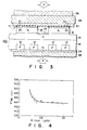
- Fig. 3 is a diagram showing the state of the aforementioned thyristor when pressure P is applied thereto.
- the soft-metal plate 30 and the cathode electrode 20 are in direct contact with each other by means of the projections 31 penetrating through the insulating film 21. Under this condition, the resistance between the soft-metal plate 30 and the cathode electrode 20 is low, ensuring a low ON voltage of the thyristor.
- the entire surface region of the soft-metal plate 30 may have the projections 31 or, as shown in Figs. 2 and 3, only that surface region of the soft-metal plate 30 which faces the cathode electrode 20 may have the same.
- the soft-metal plate 30 which is made of copper is subjected to etching using acid (HCl) in order to provide it with the projections 31.
- the inventors made packages which had the sturcture identical to that one shown in Fig. 1, and which were identical to one another, except that they have soft-metal plates having different surface roughnesses. These packages were tested, supplying a current I TM of 3000A, and maintaining the packages at temperature of 25°C, thereby detecting their ON voltages. The results of the test were as is shown in Fig. 4, wherein the ON voltages are plotted on the ordinate, and the maximun height Rmax" of the projections 31 are plotted on the abscissa.
- the soft-metal plate 30 has scratches of depths equal to or greater than 0.5 ⁇ m, the soft-metal plate 30 can be regarded as having a maximum height Rmax of 0.5 ⁇ m.
- Rmax a maximum height of 0.5 ⁇ m.
- Fig. 5 shows in cross section an example of a modification of the soft-metal plate 30 used in the first embodiment.
- the soft-metal plate 30 having the projections 31 may be covered by a coaing film 50 which is made of gold (Au), for example.
- the soft-metal plate 30 covered by the coating film 50 can be obtained by subjecting the soft-metal plate 30, made of copper, to etching, using acid in order to provide the plate 30 with the projections 31, and by thereafter plating it with gold for example.
- the coating film 50 which is made of a conductive and inactive material such as gold on the copper plate 30, the plate 30 can be successfully protected from oxygen contained in the atmosphere, thus preventing the plate 30 from oxidizing.
- Fig. 6 is a cross-sectional view of the press-contact type semiconductor device according to the second embodiment of the present invention.
- a pellet 200 in which a power transistor is formed, is employed in place of the pellet 100 in which a GTO thyristor is formed.
- the pellet 200 includes an N-type collector layer 64 consisting of an N + -type silicon layer 60 and an N-type silicon layer 62, a P-type base layer 66 which is formed on the N-type collector layer 64, and an N-type emitter layer 68 which is formed in a mesa shape on the P-type base layer 66.
- An emitter electrode 70 which is made of aluminum is formed on the N-type emitter layer 68, a base electrode 72 which is also made of aluminum is formed on the P-type base layer 66, and a collector electrode 74 which is also made of aluminum is formed on the N-type collector layer 64.
- Each of these electrodes 70, 72, and 74 is covered by an insulating film made of aluminum. In Fig. 6, only the insulating film covering the emitter electrode 70 is shown with a reference numeral 71.
- a low ON voltage can be attained by employing the soft-metal plate 30 having projections 31.
- Fig. 7 is a cross-sectional view of the press-contact semiconductor device according to the third embodiment of the present invention.
- a pellet 300 in which an IGBT is formed, is employed as shown in Fig. 7.
- the pellet 300 includes a P + -type anode layer 80, an N-type collector layer 82 which is formed on the P + -type anode layer 80, a P-type base layer 84 which is formed in the N-type collector layer 82, and an N-type source layer 86 which is formed in the P + -type base layer 84.
- a gate electrode 90 is formed above the P-type base layer 84 located between the N-type collector layer 82 and the N-type source layer 86, with a gate insulating film 88 present under the gate electrode 90.
- An insulating film 91 is formed so as to cover the gate electrode 90.
- a cathode electrode 92 made of aluminum is formed on the P-type base layer 84 and the N-type source layer 86.
- An anode electrode 94 which is made of aluminum is formed on the P + -type anode layer 80.
- Each of these electrodes 92 and 94 is covered by an insulating film made of alumina. In Fig. 7, only the insulating film covering the electrode 92 is shown with reference numeral 93.
- a low ON voltage can be attained by employing the soft-metal plate 30 having projections 31.
- Figs. 8A to 8D are diagrams which show progressive steps in producing the soft-metal plate 30.
- a photoresist film 106 is formed on a copper plate 104 by a photo-etching method, as is shown in Fig. 8A, after which the copper plate 104 is subjected to patterning, with the photoresist film 106 used as a mask, thereby obtaining a disk-shaped soft-metal plate 30 having an opening 108 formed in its central portion, as shown in Fig. 8B.
- the opening 108 is one into which the gate lead shown in Fig. 1 is inserted.
- the soft-metal plate 30 is immersed in an etchant 110 of hydrochloric acid for 20 minutes, and 70°C - 90°C (the plate 30 may be immersed for 15 minutes in an etchant of phosphoric acid series, e.g. phosphoric acid plus H 2 O 2 plus H 2 O), after which it is subjected to etching, with the result that the soft-metal plate 3 having projections 31 is obtained, as is shown in Fig. 8D.
- phosphoric acid series e.g. phosphoric acid plus H 2 O 2 plus H 2 O
- the soft-metal plate 30 is plated with gold after the step shown in Fig. 8D, the soft-metal plate 30 shown in Fig. 5 which is covered by the coating film 50 can be obtained.
- Fig. 9A is an enlarged view of a surface of the soft-metal plate 30 before being subjected to etching using the etchant (hydrochloric acid) 110
- Fig. 9B is an enlarged view of a surface of the soft-metal plate 30 after being subjected thereto.
- Fig. 10 is the cross-section of the soft-metal plate 30 which is taken along the line 10-10 shown in Fig. 9B.
- Fig. 11A is an enlarged view of a surface of the soft-metal plate 30 before being subjected to the etchant 110 (phosphoric acid series), and Fig. 11B is an enlarged view of a surface of the soft-metal plate 30 after being subjected thereto.
- Fig. 12 is the cross section of the soft-metal plate 30 which is taken along the line 12-12 shown in Fig. 11B.
- projections 31 are formed in accordance with scratches 202 which are formed mainly by a reduction roll.
- projections 31 are formed in accordance with crystal grains 204.
- the shape of the projections 31 depends upon crystal orientation.
- the projections 31 can be formed using each of a hydrochloric acid etchant and a phosphoric acid series etchant.
- a phosphoric acid series etchant it is preferable to use a phosphoric acid series etchant.
- copper is suitable for use as the material of the soft-metal plate 30, since copper is low in price and therefore best when producing a large number of soft-metal plates.
Claims (9)
- Dispositif à semi-conducteur du type à contact par pression, comprenant :une pastille (100, 200, 300) ayant des surfaces supérieure et inférieure, la pastille ayant une partie mesa formée à sa surface supérieure, la surface inférieure étant plate, et un élément semi-conducteur étant formé dans la pastille,un boîtier (40) qui entoure la pastille (100, 200, 300),une première électrode de pastille (20) formée d'aluminium sur la partie mesa de la pastille (100, 200, 300),un film isolant (21) formé d'alumine et recouvrant la première électrode de pastille (20),une seconde électrode de pastille (24) formée à la surface inférieure de la pastille (100, 200, 300),un premier plot d'électrode (26) formé dans le boîtier (40) afin qu'il soit disposé au-dessus de la première électrode de pastille (20) et auquel une pression (P) est appliquée,un second plot (32) d'électrode placé dans le boîtier (40) afin qu'il se trouve sous la seconde électrode de pastille (24), la pression (P) étant appliquée à ce plot, etune plaque (30) de métal tendre placée entre la première électrode de pastille (20) et le premier plot d'électrode (26) et ayant des saillies (31) le long de sa surface.
- Dispositif à semi-conducteur du type à contact par pression selon la revendication 1, caractérisé en ce que les saillies (31) ont une hauteur maximale de 0,5 µm ou plus pour une longueur de référence de 0,25 mm.
- Dispositif à semi-conducteur du type à contact par pression selon la revendication 1, caractérisé en ce que la plaque (30) de métal tendre est formée de cuivre.
- Dispositif à semi-conducteur du type à contact par pression selon la revendication 1, caractérisé en ce que l'élément semi-conducteur formé dans la pastille (100) est un thyristor.
- Dispositif à semi-conducteur du type à contact par pression selon la revendication 1, caractérisé en ce que l'élément semi-conducteur formé dans la pastille (200) est un transistor bipolaire.
- Dispositif à semi-conducteur du type à contact par pression selon la revendication 1, caractérisé en ce que l'élément semi-conducteur formé dans la pastille (300) est un transistor IGBT.
- Dispositif à semi-conducteur du type à contact par pression selon la revendication 1, comprenant en outre :une première plaque d'électrode (28) placée entre le premier plot d'électrode (26) et la plaque (30) de métal tendre, etune seconde plaque d'électrode (34) placée entre le second plot d'électrode (32) et la seconde électrode de pastille (24).
- Dispositif à semi-conducteur du type à contact par pression selon la revendication 1, caractérisé en ce que la plaque (30) de métal tendre est recouverte d'un film conducteur et inactif (50) de revêtement.
- Dispositif à semi-conducteur du type à contact par pression selon la revendication 8, caractérisé en ce que le film (50) de revêtement est formé d'or.
Applications Claiming Priority (4)
| Application Number | Priority Date | Filing Date | Title |
|---|---|---|---|
| JP251549/90 | 1990-09-20 | ||
| JP25154990 | 1990-09-20 | ||
| JP227109/91 | 1991-09-06 | ||
| JP22710991A JP3137375B2 (ja) | 1990-09-20 | 1991-09-06 | 圧接型半導体装置 |
Publications (3)
| Publication Number | Publication Date |
|---|---|
| EP0476661A2 EP0476661A2 (fr) | 1992-03-25 |
| EP0476661A3 EP0476661A3 (en) | 1992-06-24 |
| EP0476661B1 true EP0476661B1 (fr) | 1997-11-19 |
Family
ID=26527516
Family Applications (1)
| Application Number | Title | Priority Date | Filing Date |
|---|---|---|---|
| EP19910115961 Expired - Lifetime EP0476661B1 (fr) | 1990-09-20 | 1991-09-19 | Dispositif semi-conducteur du type à contact par pression |
Country Status (4)
| Country | Link |
|---|---|
| US (1) | US5360985A (fr) |
| EP (1) | EP0476661B1 (fr) |
| JP (1) | JP3137375B2 (fr) |
| DE (1) | DE69128226T2 (fr) |
Families Citing this family (15)
| Publication number | Priority date | Publication date | Assignee | Title |
|---|---|---|---|---|
| JP3258200B2 (ja) * | 1995-05-31 | 2002-02-18 | 株式会社東芝 | 圧接型半導体装置 |
| DE4227063A1 (de) * | 1992-08-15 | 1994-02-17 | Abb Research Ltd | Abschaltbares Hochleistungs-Halbleiterbauelement |
| JP2804216B2 (ja) * | 1993-06-22 | 1998-09-24 | 株式会社日立製作所 | ゲートターンオフサイリスタ |
| JP3180863B2 (ja) * | 1993-07-27 | 2001-06-25 | 富士電機株式会社 | 加圧接触形半導体装置およびその組立方法 |
| JP3256636B2 (ja) * | 1994-09-15 | 2002-02-12 | 株式会社東芝 | 圧接型半導体装置 |
| JP3588503B2 (ja) * | 1995-06-20 | 2004-11-10 | 株式会社東芝 | 圧接型半導体装置 |
| JP3319569B2 (ja) * | 1996-05-31 | 2002-09-03 | 株式会社東芝 | 圧接型半導体装置 |
| DE19800469A1 (de) * | 1998-01-09 | 1999-07-15 | Asea Brown Boveri | Niederinduktiv angesteuerter, gategesteuerter Thyristor |
| CN1236982A (zh) * | 1998-01-22 | 1999-12-01 | 株式会社日立制作所 | 压力接触型半导体器件及其转换器 |
| DE10258565B3 (de) * | 2002-12-14 | 2004-08-12 | Semikron Elektronik Gmbh | Schaltungsanordnung für Halbleiterbauelemente und Verfahren zur Herstellung |
| US7447041B2 (en) * | 2007-03-01 | 2008-11-04 | Delphi Technologies, Inc. | Compression connection for vertical IC packages |
| US8911087B2 (en) | 2011-05-20 | 2014-12-16 | Eyefluence, Inc. | Systems and methods for measuring reactions of head, eyes, eyelids and pupils |
| JP5899952B2 (ja) * | 2012-01-19 | 2016-04-06 | 株式会社明電舎 | 半導体モジュール |
| EP3324432A1 (fr) * | 2016-11-17 | 2018-05-23 | Infineon Technologies AG | Procédé de mise en contact électrique plusieurs puces à semi-conducteurs |
| CN113223959B (zh) * | 2021-04-12 | 2023-03-31 | 黄山芯微电子股份有限公司 | 一种压接式二极管管芯制作方法 |
Family Cites Families (12)
| Publication number | Priority date | Publication date | Assignee | Title |
|---|---|---|---|---|
| US3893153A (en) * | 1974-01-10 | 1975-07-01 | Westinghouse Electric Corp | Light activated thyristor with high di/dt capability |
| US4127863A (en) * | 1975-10-01 | 1978-11-28 | Tokyo Shibaura Electric Co., Ltd. | Gate turn-off type thyristor with separate semiconductor resistive wafer providing emitter ballast |
| DE2556469C3 (de) * | 1975-12-15 | 1978-09-07 | Siemens Ag, 1000 Berlin Und 8000 Muenchen | Halbleiterbauelement mit Druckkontakt |
| JPS5495183A (en) * | 1978-01-13 | 1979-07-27 | Mitsubishi Electric Corp | Pressure contact-type semiconductor device |
| JPS5578535A (en) * | 1978-12-08 | 1980-06-13 | Mitsubishi Electric Corp | Pressure-contact type semiconductor device |
| DE2926756C2 (de) * | 1979-07-03 | 1984-03-22 | Licentia Patent-Verwaltungs-Gmbh, 6000 Frankfurt | Schottky-Dioden-Anordnung |
| JPH081914B2 (ja) * | 1987-03-31 | 1996-01-10 | 株式会社東芝 | 圧接型半導体装置 |
| GB2215125B (en) * | 1988-02-22 | 1991-04-24 | Mitsubishi Electric Corp | Semiconductor device |
| EP0347561B1 (fr) * | 1988-06-21 | 1994-03-16 | International Business Machines Corporation | Connexion électrique séparable |
| US4937653A (en) * | 1988-07-21 | 1990-06-26 | American Telephone And Telegraph Company | Semiconductor integrated circuit chip-to-chip interconnection scheme |
| JPH0693468B2 (ja) * | 1988-08-09 | 1994-11-16 | 株式会社東芝 | 圧接平型半導体装置 |
| JP2739970B2 (ja) * | 1988-10-19 | 1998-04-15 | 株式会社東芝 | 圧接型半導体装置 |
-
1991
- 1991-09-06 JP JP22710991A patent/JP3137375B2/ja not_active Expired - Fee Related
- 1991-09-19 EP EP19910115961 patent/EP0476661B1/fr not_active Expired - Lifetime
- 1991-09-19 DE DE1991628226 patent/DE69128226T2/de not_active Expired - Fee Related
-
1993
- 1993-06-01 US US08/070,040 patent/US5360985A/en not_active Expired - Lifetime
Also Published As
| Publication number | Publication date |
|---|---|
| JPH0541514A (ja) | 1993-02-19 |
| DE69128226T2 (de) | 1998-04-16 |
| EP0476661A2 (fr) | 1992-03-25 |
| US5360985A (en) | 1994-11-01 |
| EP0476661A3 (en) | 1992-06-24 |
| JP3137375B2 (ja) | 2001-02-19 |
| DE69128226D1 (de) | 1998-01-02 |
Similar Documents
| Publication | Publication Date | Title |
|---|---|---|
| EP0476661B1 (fr) | Dispositif semi-conducteur du type à contact par pression | |
| CN1016298B (zh) | 为非平面型半导体器件形成顶部接触 | |
| US4996586A (en) | Crimp-type semiconductor device having non-alloy structure | |
| US4100566A (en) | Resin-sealed type semiconductor devices and manufacturing method of the same | |
| EP0285074B1 (fr) | Dispositif semi-conducteur du type de contact par pression | |
| US20070007614A1 (en) | Schottky diode with improved surge capability | |
| US4963970A (en) | Vertical MOSFET device having protector | |
| US4246596A (en) | High current press pack semiconductor device having a mesa structure | |
| US4402004A (en) | High current press pack semiconductor device having a mesa structure | |
| JP2006173437A (ja) | 半導体装置 | |
| US4388635A (en) | High breakdown voltage semiconductor device | |
| TW200409355A (en) | Chip-scale schottky device | |
| KR850006654A (ko) | 반도체 장치 | |
| EP0064231B1 (fr) | Dispositif semiconducteur à compression | |
| KR940008217B1 (ko) | 전력용 압접형 반도체장치 | |
| EP0043818A1 (fr) | Procede et appareil d'elimination d'eau et de substances de contamination electrochimique active environnantes semblables dans des dispositifs a semi-conducteurs, et autres dispositifs electroniques et electriques | |
| EP0677877B1 (fr) | Dispositif semi-conducteur à grille isolée et inverseur de puissance utilisant un tel dispositif | |
| EP0431586A2 (fr) | Dispositif semi-conducteur de haute puissance | |
| JPH0142498B2 (fr) | ||
| EP0235706B1 (fr) | Thyristor comportant un élément résistif couplé à sa grille et méthode de fabrication | |
| KR960000709B1 (ko) | 압접형 반도체장치 | |
| JPH0897406A (ja) | ゲートターンオフサイリスタおよび半導体素子 | |
| JP2604997B2 (ja) | 圧接型半導体装置 | |
| GB2168529A (en) | Electrical contacts for semiconductor devices | |
| JPH065685B2 (ja) | 加圧接触形半導体装置 |
Legal Events
| Date | Code | Title | Description |
|---|---|---|---|
| PUAI | Public reference made under article 153(3) epc to a published international application that has entered the european phase |
Free format text: ORIGINAL CODE: 0009012 |
|
| 17P | Request for examination filed |
Effective date: 19910919 |
|
| AK | Designated contracting states |
Kind code of ref document: A2 Designated state(s): DE FR GB |
|
| PUAL | Search report despatched |
Free format text: ORIGINAL CODE: 0009013 |
|
| AK | Designated contracting states |
Kind code of ref document: A3 Designated state(s): DE FR GB |
|
| 17Q | First examination report despatched |
Effective date: 19941108 |
|
| GRAG | Despatch of communication of intention to grant |
Free format text: ORIGINAL CODE: EPIDOS AGRA |
|
| GRAH | Despatch of communication of intention to grant a patent |
Free format text: ORIGINAL CODE: EPIDOS IGRA |
|
| GRAH | Despatch of communication of intention to grant a patent |
Free format text: ORIGINAL CODE: EPIDOS IGRA |
|
| GRAA | (expected) grant |
Free format text: ORIGINAL CODE: 0009210 |
|
| AK | Designated contracting states |
Kind code of ref document: B1 Designated state(s): DE FR GB |
|
| REF | Corresponds to: |
Ref document number: 69128226 Country of ref document: DE Date of ref document: 19980102 |
|
| ET | Fr: translation filed | ||
| PLBE | No opposition filed within time limit |
Free format text: ORIGINAL CODE: 0009261 |
|
| STAA | Information on the status of an ep patent application or granted ep patent |
Free format text: STATUS: NO OPPOSITION FILED WITHIN TIME LIMIT |
|
| REG | Reference to a national code |
Ref country code: GB Ref legal event code: 746 Effective date: 19980915 |
|
| 26N | No opposition filed | ||
| REG | Reference to a national code |
Ref country code: FR Ref legal event code: D6 |
|
| REG | Reference to a national code |
Ref country code: GB Ref legal event code: IF02 |
|
| PGFP | Annual fee paid to national office [announced via postgrant information from national office to epo] |
Ref country code: FR Payment date: 20080915 Year of fee payment: 18 |
|
| PGFP | Annual fee paid to national office [announced via postgrant information from national office to epo] |
Ref country code: GB Payment date: 20080924 Year of fee payment: 18 |
|
| PGFP | Annual fee paid to national office [announced via postgrant information from national office to epo] |
Ref country code: DE Payment date: 20081002 Year of fee payment: 18 |
|
| GBPC | Gb: european patent ceased through non-payment of renewal fee |
Effective date: 20090919 |
|
| REG | Reference to a national code |
Ref country code: FR Ref legal event code: ST Effective date: 20100531 |
|
| PG25 | Lapsed in a contracting state [announced via postgrant information from national office to epo] |
Ref country code: DE Free format text: LAPSE BECAUSE OF NON-PAYMENT OF DUE FEES Effective date: 20100401 Ref country code: FR Free format text: LAPSE BECAUSE OF NON-PAYMENT OF DUE FEES Effective date: 20090930 |
|
| PG25 | Lapsed in a contracting state [announced via postgrant information from national office to epo] |
Ref country code: GB Free format text: LAPSE BECAUSE OF NON-PAYMENT OF DUE FEES Effective date: 20090919 |