EP0431586A2 - Dispositif semi-conducteur de haute puissance - Google Patents
Dispositif semi-conducteur de haute puissance Download PDFInfo
- Publication number
- EP0431586A2 EP0431586A2 EP19900123304 EP90123304A EP0431586A2 EP 0431586 A2 EP0431586 A2 EP 0431586A2 EP 19900123304 EP19900123304 EP 19900123304 EP 90123304 A EP90123304 A EP 90123304A EP 0431586 A2 EP0431586 A2 EP 0431586A2
- Authority
- EP
- European Patent Office
- Prior art keywords
- conductive layer
- thinner
- semiconductor device
- conductive layers
- terminal
- Prior art date
- Legal status (The legal status is an assumption and is not a legal conclusion. Google has not performed a legal analysis and makes no representation as to the accuracy of the status listed.)
- Granted
Links
Images


Classifications
-
- H—ELECTRICITY
- H01—ELECTRIC ELEMENTS
- H01L—SEMICONDUCTOR DEVICES NOT COVERED BY CLASS H10
- H01L23/00—Details of semiconductor or other solid state devices
- H01L23/58—Structural electrical arrangements for semiconductor devices not otherwise provided for, e.g. in combination with batteries
- H01L23/62—Protection against overvoltage, e.g. fuses, shunts
-
- H—ELECTRICITY
- H01—ELECTRIC ELEMENTS
- H01L—SEMICONDUCTOR DEVICES NOT COVERED BY CLASS H10
- H01L23/00—Details of semiconductor or other solid state devices
-
- H—ELECTRICITY
- H01—ELECTRIC ELEMENTS
- H01L—SEMICONDUCTOR DEVICES NOT COVERED BY CLASS H10
- H01L2224/00—Indexing scheme for arrangements for connecting or disconnecting semiconductor or solid-state bodies and methods related thereto as covered by H01L24/00
- H01L2224/01—Means for bonding being attached to, or being formed on, the surface to be connected, e.g. chip-to-package, die-attach, "first-level" interconnects; Manufacturing methods related thereto
- H01L2224/02—Bonding areas; Manufacturing methods related thereto
- H01L2224/04—Structure, shape, material or disposition of the bonding areas prior to the connecting process
- H01L2224/05—Structure, shape, material or disposition of the bonding areas prior to the connecting process of an individual bonding area
- H01L2224/0554—External layer
- H01L2224/0555—Shape
- H01L2224/05552—Shape in top view
- H01L2224/05553—Shape in top view being rectangular
-
- H—ELECTRICITY
- H01—ELECTRIC ELEMENTS
- H01L—SEMICONDUCTOR DEVICES NOT COVERED BY CLASS H10
- H01L2224/00—Indexing scheme for arrangements for connecting or disconnecting semiconductor or solid-state bodies and methods related thereto as covered by H01L24/00
- H01L2224/01—Means for bonding being attached to, or being formed on, the surface to be connected, e.g. chip-to-package, die-attach, "first-level" interconnects; Manufacturing methods related thereto
- H01L2224/42—Wire connectors; Manufacturing methods related thereto
- H01L2224/44—Structure, shape, material or disposition of the wire connectors prior to the connecting process
- H01L2224/45—Structure, shape, material or disposition of the wire connectors prior to the connecting process of an individual wire connector
- H01L2224/45001—Core members of the connector
- H01L2224/45099—Material
- H01L2224/451—Material with a principal constituent of the material being a metal or a metalloid, e.g. boron (B), silicon (Si), germanium (Ge), arsenic (As), antimony (Sb), tellurium (Te) and polonium (Po), and alloys thereof
-
- H—ELECTRICITY
- H01—ELECTRIC ELEMENTS
- H01L—SEMICONDUCTOR DEVICES NOT COVERED BY CLASS H10
- H01L2224/00—Indexing scheme for arrangements for connecting or disconnecting semiconductor or solid-state bodies and methods related thereto as covered by H01L24/00
- H01L2224/01—Means for bonding being attached to, or being formed on, the surface to be connected, e.g. chip-to-package, die-attach, "first-level" interconnects; Manufacturing methods related thereto
- H01L2224/42—Wire connectors; Manufacturing methods related thereto
- H01L2224/47—Structure, shape, material or disposition of the wire connectors after the connecting process
- H01L2224/48—Structure, shape, material or disposition of the wire connectors after the connecting process of an individual wire connector
- H01L2224/4805—Shape
- H01L2224/4809—Loop shape
- H01L2224/48091—Arched
-
- H—ELECTRICITY
- H01—ELECTRIC ELEMENTS
- H01L—SEMICONDUCTOR DEVICES NOT COVERED BY CLASS H10
- H01L2224/00—Indexing scheme for arrangements for connecting or disconnecting semiconductor or solid-state bodies and methods related thereto as covered by H01L24/00
- H01L2224/01—Means for bonding being attached to, or being formed on, the surface to be connected, e.g. chip-to-package, die-attach, "first-level" interconnects; Manufacturing methods related thereto
- H01L2224/42—Wire connectors; Manufacturing methods related thereto
- H01L2224/47—Structure, shape, material or disposition of the wire connectors after the connecting process
- H01L2224/48—Structure, shape, material or disposition of the wire connectors after the connecting process of an individual wire connector
- H01L2224/481—Disposition
- H01L2224/48151—Connecting between a semiconductor or solid-state body and an item not being a semiconductor or solid-state body, e.g. chip-to-substrate, chip-to-passive
- H01L2224/48221—Connecting between a semiconductor or solid-state body and an item not being a semiconductor or solid-state body, e.g. chip-to-substrate, chip-to-passive the body and the item being stacked
- H01L2224/48225—Connecting between a semiconductor or solid-state body and an item not being a semiconductor or solid-state body, e.g. chip-to-substrate, chip-to-passive the body and the item being stacked the item being non-metallic, e.g. insulating substrate with or without metallisation
- H01L2224/48227—Connecting between a semiconductor or solid-state body and an item not being a semiconductor or solid-state body, e.g. chip-to-substrate, chip-to-passive the body and the item being stacked the item being non-metallic, e.g. insulating substrate with or without metallisation connecting the wire to a bond pad of the item
-
- H—ELECTRICITY
- H01—ELECTRIC ELEMENTS
- H01L—SEMICONDUCTOR DEVICES NOT COVERED BY CLASS H10
- H01L2224/00—Indexing scheme for arrangements for connecting or disconnecting semiconductor or solid-state bodies and methods related thereto as covered by H01L24/00
- H01L2224/01—Means for bonding being attached to, or being formed on, the surface to be connected, e.g. chip-to-package, die-attach, "first-level" interconnects; Manufacturing methods related thereto
- H01L2224/42—Wire connectors; Manufacturing methods related thereto
- H01L2224/47—Structure, shape, material or disposition of the wire connectors after the connecting process
- H01L2224/48—Structure, shape, material or disposition of the wire connectors after the connecting process of an individual wire connector
- H01L2224/484—Connecting portions
- H01L2224/4847—Connecting portions the connecting portion on the bonding area of the semiconductor or solid-state body being a wedge bond
- H01L2224/48472—Connecting portions the connecting portion on the bonding area of the semiconductor or solid-state body being a wedge bond the other connecting portion not on the bonding area also being a wedge bond, i.e. wedge-to-wedge
-
- H—ELECTRICITY
- H01—ELECTRIC ELEMENTS
- H01L—SEMICONDUCTOR DEVICES NOT COVERED BY CLASS H10
- H01L24/00—Arrangements for connecting or disconnecting semiconductor or solid-state bodies; Methods or apparatus related thereto
- H01L24/01—Means for bonding being attached to, or being formed on, the surface to be connected, e.g. chip-to-package, die-attach, "first-level" interconnects; Manufacturing methods related thereto
- H01L24/42—Wire connectors; Manufacturing methods related thereto
- H01L24/44—Structure, shape, material or disposition of the wire connectors prior to the connecting process
- H01L24/45—Structure, shape, material or disposition of the wire connectors prior to the connecting process of an individual wire connector
-
- H—ELECTRICITY
- H01—ELECTRIC ELEMENTS
- H01L—SEMICONDUCTOR DEVICES NOT COVERED BY CLASS H10
- H01L24/00—Arrangements for connecting or disconnecting semiconductor or solid-state bodies; Methods or apparatus related thereto
- H01L24/01—Means for bonding being attached to, or being formed on, the surface to be connected, e.g. chip-to-package, die-attach, "first-level" interconnects; Manufacturing methods related thereto
- H01L24/42—Wire connectors; Manufacturing methods related thereto
- H01L24/47—Structure, shape, material or disposition of the wire connectors after the connecting process
- H01L24/48—Structure, shape, material or disposition of the wire connectors after the connecting process of an individual wire connector
-
- H—ELECTRICITY
- H01—ELECTRIC ELEMENTS
- H01L—SEMICONDUCTOR DEVICES NOT COVERED BY CLASS H10
- H01L2924/00—Indexing scheme for arrangements or methods for connecting or disconnecting semiconductor or solid-state bodies as covered by H01L24/00
- H01L2924/0001—Technical content checked by a classifier
- H01L2924/00014—Technical content checked by a classifier the subject-matter covered by the group, the symbol of which is combined with the symbol of this group, being disclosed without further technical details
-
- H—ELECTRICITY
- H01—ELECTRIC ELEMENTS
- H01L—SEMICONDUCTOR DEVICES NOT COVERED BY CLASS H10
- H01L2924/00—Indexing scheme for arrangements or methods for connecting or disconnecting semiconductor or solid-state bodies as covered by H01L24/00
- H01L2924/01—Chemical elements
- H01L2924/01014—Silicon [Si]
-
- H—ELECTRICITY
- H01—ELECTRIC ELEMENTS
- H01L—SEMICONDUCTOR DEVICES NOT COVERED BY CLASS H10
- H01L2924/00—Indexing scheme for arrangements or methods for connecting or disconnecting semiconductor or solid-state bodies as covered by H01L24/00
- H01L2924/10—Details of semiconductor or other solid state devices to be connected
- H01L2924/1015—Shape
- H01L2924/1016—Shape being a cuboid
- H01L2924/10161—Shape being a cuboid with a rectangular active surface
-
- H—ELECTRICITY
- H01—ELECTRIC ELEMENTS
- H01L—SEMICONDUCTOR DEVICES NOT COVERED BY CLASS H10
- H01L2924/00—Indexing scheme for arrangements or methods for connecting or disconnecting semiconductor or solid-state bodies as covered by H01L24/00
- H01L2924/10—Details of semiconductor or other solid state devices to be connected
- H01L2924/11—Device type
- H01L2924/13—Discrete devices, e.g. 3 terminal devices
- H01L2924/1301—Thyristor
-
- H—ELECTRICITY
- H01—ELECTRIC ELEMENTS
- H01L—SEMICONDUCTOR DEVICES NOT COVERED BY CLASS H10
- H01L2924/00—Indexing scheme for arrangements or methods for connecting or disconnecting semiconductor or solid-state bodies as covered by H01L24/00
- H01L2924/10—Details of semiconductor or other solid state devices to be connected
- H01L2924/11—Device type
- H01L2924/13—Discrete devices, e.g. 3 terminal devices
- H01L2924/1304—Transistor
- H01L2924/1305—Bipolar Junction Transistor [BJT]
- H01L2924/13055—Insulated gate bipolar transistor [IGBT]
-
- H—ELECTRICITY
- H01—ELECTRIC ELEMENTS
- H01L—SEMICONDUCTOR DEVICES NOT COVERED BY CLASS H10
- H01L2924/00—Indexing scheme for arrangements or methods for connecting or disconnecting semiconductor or solid-state bodies as covered by H01L24/00
- H01L2924/10—Details of semiconductor or other solid state devices to be connected
- H01L2924/11—Device type
- H01L2924/13—Discrete devices, e.g. 3 terminal devices
- H01L2924/1304—Transistor
- H01L2924/1306—Field-effect transistor [FET]
- H01L2924/13091—Metal-Oxide-Semiconductor Field-Effect Transistor [MOSFET]
-
- H—ELECTRICITY
- H01—ELECTRIC ELEMENTS
- H01L—SEMICONDUCTOR DEVICES NOT COVERED BY CLASS H10
- H01L2924/00—Indexing scheme for arrangements or methods for connecting or disconnecting semiconductor or solid-state bodies as covered by H01L24/00
- H01L2924/10—Details of semiconductor or other solid state devices to be connected
- H01L2924/11—Device type
- H01L2924/14—Integrated circuits
Definitions
- This invention relates to a high-power semiconductor device sealed within resin, and more particularly to a high-power semiconductor device which can generate an overcurrent detecting signal, requiring no external elements.
- a conventional high power semiconductor device will be described with reference to Figs. 1A, 1B, and 1C.
- the rated current of the device is several amperes and more.
- a conductive layer for example, copper plate 2 is adhered to the surface of insulating substrate 1.
- Semiconductor element 3 is soldered on copper plate 2.
- Conductive layers 4 and 5 made of copper plates are adhered to the surface of insulating layer 1 on the both sides of copper plate 2.
- Electrodes 6 and 7 are formed on semiconductor element 3 and electrically connected to conductive layers 4 and 5, respectively, by fine wires 8 and 9 made of metal, by means of a known wire bonding method or a ultrasonic bonding method.
- Terminals C, E, and G are adhered to the conductive layers, i.e., copper plates 2, 4, and 5.
- Fig. 1B is a perspective view of the final product, in which terminals C, E, and G protrude from the rectangular sealing resin layer.
- the emitter of semiconductor element 3 is connected to terminal E, the gate thereof to terminal G, and the collector thereof to terminal C, for example, as shown in Fig. 1C illustrating an insulated gate bipolar transistor (IGBT). In this way, high-power semiconductor device 11 is formed.
- IGBT insulated gate bipolar transistor
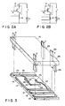
- resistor 12 (see Fig. 2A) or current transformer 13 (see Fig. 2B) is electrically connected to high power semiconductor device 11 enclosed by broken lines, and detects a current.
- reference symbols L and V denote a load and a power source, respectively.
- resistor 12 When resistor 12 detects a current as is shown in Fig. 2A, power of the product of the square of the current and the resistance is lost. To suppress such a loss of power, a resistor having considerably low resistance is used in general. However, a low resistance resistor is not easily available and expensive. In addition, the resistor must be large, so as to withstand to Joule heat generated in the resistor.
- the conventional method of detecting a current is disadvantageous in that an external element for detecting an overcurrent must be connected thereto, and the element is expensive. Moreover, since an external element must be used, the entire system including the semiconductor device tends to be large and difficult to handle.
- an object of the present invention is to provide a high-power semiconductor device which requires no external elements for detecting a current.
- Another object of the present invention is to provide an inexpensive and compact high-power semiconductor device which can generate an overcurrent detecting signal.
- a high-power semiconductor device comprising a plurality of conductive layers selectively adhered to a surface of an insulating substrate, a semiconductor element having a plurality of electrodes connected to the conductive layers, terminals electrically connected to the electrodes, and a sealing resin layer covering the above-mentioned components, the semiconductor device further comprising an overcurrent detecting terminal, and characterized in that at least one of the conductive layers has at least a portion which is thinner than the other conductive layers, the terminals for one of the electrodes is connected to an end of the conductive layer having a thinner portion, and the overcurrent detecting terminal is electrically connected to said one of the electrodes and to the other end of the conductive layer having a thinner portion.
- Fig. 1A is a perspective view showing a primary portion of a conventional high-power semiconductor device
- Fig. 1B is a perspective view showing an exterior of the conventional high-power semiconductor device sealed with resin
- Fig. 1C is a diagram showing an equivalent circuit of the conventional high power semiconductor device
- Figs. 2A and 2B are diagrams showing equivalent circuits of conventional devices for detecting an overcurrent
- Fig. 3 is a perspective view showing a step of assembling a high power semiconductor device according to an embodiment of the present invention
- Figs. 4, 5, and 6 are perspective views showing a high power semiconductor device according to other embodiments of the present invention.
- assembly 16 has terminal E (emitter), terminal C (collector), terminal G (gate), and overcurrent detecting terminal T, all of which are attached to sealing resin plate 28.
- Conductive layers for example, copper plates, 19, 20, 21 and 22 are adhered to an insulating substrate, or ceramic substrate 18 formed of alumina and aluminum nitride. At least one of the conductive layers is thinner than the others. In the embodiment layer 22 is thinner than the others.
- Conductive layers 19, 20, 21 and 22 are adhered to ceramic substrate 18 by a direct bonding method, i.e., cuprous oxide plates are heated and adhered to ceramic substrate, thereby forming conductive layers 19, 20, 21 and 22.
- the conductive layers can be formed of metallized layers, or can be formed by a screen printing method. It is desirable that thicker conductive layers 19, 20 and 21 be 0.5 to 0.3 mm thick and thinner conductive layer 22 be 10 to 100 ⁇ m thick.
- Insulator element 23 for example, an insulated gate bipolar transistor (IGBT) for use in a high power device, is mounted on conductive layer 19 by soldering.
- IGBT insulated gate bipolar transistor
- the IGBT is only an example of various semiconductor elements, and can be replaced by other high power semiconductor devices such as high-power Darlington transistor, a high power transistor thyristor, or a power MOS transistor.
- Gate electrode 24 and emitter electrode 25 are formed on the surface of high-power semiconductor element 23.
- the top face of semiconductor element 23 generally has an insulating layer or a conductive metal layer formed thereon, so these layers are referred to as "the surface”.
- the electrodes in the present invention are electrically connected to areas isolated by PN junctions which are formed by injecting or diffusing a predetermined amount of impurities into the silicon substrate, for example.
- Gate electrode 24 and emitter electrode 25 are respectively connected to conductive layers 20 and 21 having the same thickness by metallic fine wires 26 and 27 by an ultrasonic bonding method or a thermocompression bonding method.
- Copper plate 19 is soldered with high-power semiconductor element 23, and serves as a collector electrode of a bipolar transistor.
- terminal G for gate electrode 24, terminal E for emitter electrode 25, collector terminal C for collector electrode and overcurrent detecting terminal T are fixed to sealing resin plate 28, thus constituting assembly 16.
- terminal T is so shaped as to be connected to both of thinner conductive layer 22 and thicker conductive layer 21 which is connected to emitter electrode 25 by metallic fine wire 27.
- terminal T consists of metal plate portion 29 which is as wide as the distance between conductive layers 21 and 22 plus the widths of layers 21 and 22, and lead-in portion 30 which is narrower than metal plate portion 29.
- Terminals G, E and C are simultaneously brought into contact with copper plates 20, 22 and 19, and soldered thereto. At the same time, metal plate portion 29 of terminal T is soldered to conductive layers 21 and 22.
- each potential of the electrodes is derived by terminal E, G or T to the exterior of the semiconductor device.
- terminal T connected to conductive layers 21 and 22 has the same potential as that of electrode 25 which is electrically connected to these conductive layers 21 and 22.
- Layer 22 has a resistance such that Joule heat generated is negligible low, but the current can be detected, that is, 1 to several tens of m ⁇ in accordance with the rating of the current.
- a voltage corresponding to the current flowing through the conductive layers is detected as a potential difference between emitter terminal E and overcurrent detecting terminal T. Since the thinner conductive layer serving as a resistor is formed on the insulating substrate having a relatively high heat conductivity, Joule heat generated from the thinner conductive layer is easily dissipated to the substrate.
- Fig. 4 shows another embodiment of the present invention, which differs from the embodiment shown Fig. 3 in that terminal C for collector electrode is connected to one of the end portions of thinner conductive layer 22.
- Overcurrent detecting terminal T is connected across conductive layer 19 and another end portions of thinner conductive layer 22.
- the overcurrent flowing through the collector circuit can be detected by measuring the voltage across terminal C and overcurrent detecting terminal T.
- Fig. 5 shows still another embodiment of the present invention.
- a center portion of thick conductive layer 31 is thinner than both end portions.
- Emitter electrode 25 of semiconductor element 23 is connected to one of the end portions, i.e. the thicker portions of conductive layer 31, by metallic fine wire 27.
- Overcurrent detecting terminal T is soldered also to the same portion.
- Terminal E is soldered to the other end portion of conductive layer 31.
- an overcurrent is detected by measuring the voltage across terminals T and E connected to the end portions of conductive layer 31, in the same manner as in the embodiment shown in Fig. 3.
- Metallic fine wire 27 is directly bonded to the above mentioned thicker portion of conductive layer 31.
- the resistance of conductive layer 31 is determined by the length of the thinner portion, so that the resistance is not changed due to the displacement of the connecting point of the fine wire.
- Fig. 6 shows further embodiment of the present invention.
- conductive layer 22 thinner than the other conductive layers is connected to or formed integral with thicker conductive layer 19.
- an end of conductive layer 22 is connected to the a portion of conductive layer 19 on which semiconductor element 23 is mounted.
- Overcurrent detecting terminal T is connected to an end portion of conductive layer 22, which is connected to thicker conductive layer 19.
- Terminal C for a electrode is connected to the other end portion of conductive layer 22.
- the overcurrent detection terminal is derived to the exterior of the sealing resin layer.
- a monolithic or a hybrid semiconductor element incorporating a feedback circuit for detecting and controlling current it is unnecessary that the overcurrent detecting terminal be derived to the exterior of the sealing resin layer.
- only one thinner conductive layer is formed on the substrate; however, if a plurality of semiconductor elements are formed, one thinner conductive layer may be formed with respect to one semiconductor element, and therefore, a plurality of thinner conductive layers can be formed on the substrate.
Applications Claiming Priority (2)
| Application Number | Priority Date | Filing Date | Title |
|---|---|---|---|
| JP318153/89 | 1989-12-07 | ||
| JP1318153A JPH0691176B2 (ja) | 1989-12-07 | 1989-12-07 | 大電力用半導体装置 |
Publications (3)
| Publication Number | Publication Date |
|---|---|
| EP0431586A2 true EP0431586A2 (fr) | 1991-06-12 |
| EP0431586A3 EP0431586A3 (en) | 1992-06-03 |
| EP0431586B1 EP0431586B1 (fr) | 1995-12-06 |
Family
ID=18096080
Family Applications (1)
| Application Number | Title | Priority Date | Filing Date |
|---|---|---|---|
| EP19900123304 Expired - Lifetime EP0431586B1 (fr) | 1989-12-07 | 1990-12-05 | Dispositif semi-conducteur de haute puissance |
Country Status (5)
| Country | Link |
|---|---|
| US (1) | US5115300A (fr) |
| EP (1) | EP0431586B1 (fr) |
| JP (1) | JPH0691176B2 (fr) |
| KR (1) | KR930005492B1 (fr) |
| DE (1) | DE69024031T2 (fr) |
Cited By (3)
| Publication number | Priority date | Publication date | Assignee | Title |
|---|---|---|---|---|
| EP0874401A2 (fr) * | 1997-04-22 | 1998-10-28 | Nec Corporation | Dispositif semiconducteur comprenant une couche conductrice de protection |
| US6724599B2 (en) | 2001-06-19 | 2004-04-20 | Mitsubishi Denki Kabushiki Kaisha | Power semiconductor device |
| DE102006005420A1 (de) * | 2006-02-03 | 2007-09-06 | Infineon Technologies Ag | Stapelbares Halbleiterbauteil und Verfahren zur Herstellung desselben |
Families Citing this family (5)
| Publication number | Priority date | Publication date | Assignee | Title |
|---|---|---|---|---|
| US5313091A (en) * | 1992-09-28 | 1994-05-17 | Sundstrand Corporation | Package for a high power electrical component |
| US5744869A (en) * | 1995-12-05 | 1998-04-28 | Motorola, Inc. | Apparatus for mounting a flip-chip semiconductor device |
| JP3837215B2 (ja) * | 1997-10-09 | 2006-10-25 | 三菱電機株式会社 | 個別半導体装置およびその製造方法 |
| JP2003258180A (ja) * | 2002-02-27 | 2003-09-12 | Sanyo Electric Co Ltd | 半導体装置の製造方法 |
| JP5205834B2 (ja) * | 2007-06-25 | 2013-06-05 | 日産自動車株式会社 | 半導体装置 |
Citations (2)
| Publication number | Priority date | Publication date | Assignee | Title |
|---|---|---|---|---|
| WO1983001153A1 (fr) * | 1981-09-14 | 1983-03-31 | Carreras, Michelle | Dispositif de protection integre contre les surtension d'un circuit electronique, et circuit electronique protege par ce dispositif |
| FR2574222A1 (fr) * | 1984-12-04 | 1986-06-06 | Sintra | Procede de fabrication d'un substrat pour circuit hybride comportant des connexions faiblement resistives |
Family Cites Families (1)
| Publication number | Priority date | Publication date | Assignee | Title |
|---|---|---|---|---|
| US4818895A (en) * | 1987-11-13 | 1989-04-04 | Kaufman Lance R | Direct current sense lead |
-
1989
- 1989-12-07 JP JP1318153A patent/JPH0691176B2/ja not_active Expired - Fee Related
-
1990
- 1990-12-05 EP EP19900123304 patent/EP0431586B1/fr not_active Expired - Lifetime
- 1990-12-05 US US07/622,591 patent/US5115300A/en not_active Expired - Lifetime
- 1990-12-05 DE DE1990624031 patent/DE69024031T2/de not_active Expired - Fee Related
- 1990-12-06 KR KR1019900020021A patent/KR930005492B1/ko not_active IP Right Cessation
Patent Citations (2)
| Publication number | Priority date | Publication date | Assignee | Title |
|---|---|---|---|---|
| WO1983001153A1 (fr) * | 1981-09-14 | 1983-03-31 | Carreras, Michelle | Dispositif de protection integre contre les surtension d'un circuit electronique, et circuit electronique protege par ce dispositif |
| FR2574222A1 (fr) * | 1984-12-04 | 1986-06-06 | Sintra | Procede de fabrication d'un substrat pour circuit hybride comportant des connexions faiblement resistives |
Non-Patent Citations (2)
| Title |
|---|
| PATENT ABSTRACTS OF JAPAN vol. 8, no. 103 (E-244)(1540) 15 May 1984 & JP-A-59 019 361 ( MITSUBISHI DENKI ) 31 January 1984 * |
| PROCEEDINGS OF THE NINTH INTERNATIONAL TELECOMMUNICATIONS ENERGY CONFERENCE 1987, NEW YORK , US pages 240 - 247; SATOSHI MORI ET AL.: 'A new 100A , 500V power MOSFET module with un-precedented di/dt ,dv/dt endurance' * |
Cited By (6)
| Publication number | Priority date | Publication date | Assignee | Title |
|---|---|---|---|---|
| EP0874401A2 (fr) * | 1997-04-22 | 1998-10-28 | Nec Corporation | Dispositif semiconducteur comprenant une couche conductrice de protection |
| EP0874401A3 (fr) * | 1997-04-22 | 1999-10-27 | Nec Corporation | Dispositif semiconducteur comprenant une couche conductrice de protection |
| US6724599B2 (en) | 2001-06-19 | 2004-04-20 | Mitsubishi Denki Kabushiki Kaisha | Power semiconductor device |
| DE10162242B4 (de) * | 2001-06-19 | 2005-02-17 | Mitsubishi Denki K.K. | Leistungshalbleiterbauelement für beispielsweise Halbbrückenschaltungen |
| DE102006005420A1 (de) * | 2006-02-03 | 2007-09-06 | Infineon Technologies Ag | Stapelbares Halbleiterbauteil und Verfahren zur Herstellung desselben |
| DE102006005420B4 (de) * | 2006-02-03 | 2010-07-15 | Infineon Technologies Ag | Stapelbares Halbleiterbauteil und Verfahren zur Herstellung desselben |
Also Published As
| Publication number | Publication date |
|---|---|
| KR930005492B1 (ko) | 1993-06-22 |
| EP0431586A3 (en) | 1992-06-03 |
| JPH03179767A (ja) | 1991-08-05 |
| DE69024031D1 (de) | 1996-01-18 |
| EP0431586B1 (fr) | 1995-12-06 |
| DE69024031T2 (de) | 1996-05-09 |
| KR910013517A (ko) | 1991-08-08 |
| US5115300A (en) | 1992-05-19 |
| JPH0691176B2 (ja) | 1994-11-14 |
Similar Documents
| Publication | Publication Date | Title |
|---|---|---|
| KR930011798B1 (ko) | 반도체장치 | |
| US5347160A (en) | Power semiconductor integrated circuit package | |
| US5682057A (en) | Semiconductor device incorporating a temperature fuse | |
| US5038194A (en) | Semiconductor device | |
| JP4220094B2 (ja) | パワー半導体モジュール | |
| US20060113562A1 (en) | Semiconductor power module having an electrically insulating heat sink and method of manufacturing the same | |
| JP2009503872A (ja) | 熱的に結合したmov過電圧要素とpptc過電流要素を有する回路保護デバイス | |
| CN112352314B (zh) | 半导体模块 | |
| US4314270A (en) | Hybrid thick film integrated circuit heat dissipating and grounding assembly | |
| EP0418891B1 (fr) | Dispositif semi-conducteur de puissance à encapsulation en plastique | |
| EP0431586B1 (fr) | Dispositif semi-conducteur de haute puissance | |
| EP0609528A1 (fr) | Empaquetage semi-conducteur à basse inductance | |
| EP0304058B1 (fr) | Montage d'un élément transistor sur cadre de connexion au moyen d'une plaque céramique | |
| JP2005129826A (ja) | パワー半導体装置 | |
| EP0340466B1 (fr) | Dispositif semi-conducteur comprenant des conducteurs | |
| CN110176446B (zh) | 半导体装置 | |
| JPH0677399A (ja) | 双方向半導体スイッチ | |
| JPH0645504A (ja) | 半導体装置 | |
| GB2038554A (en) | Thyristor | |
| JP3477002B2 (ja) | 半導体装置 | |
| EP0181975B1 (fr) | Dispositif semi-conducteur comprenant un corps de support | |
| JP3311935B2 (ja) | 半導体装置およびその計測方法 | |
| JPH0648874Y2 (ja) | 半導体装置 | |
| JPH06120271A (ja) | 半導体装置 | |
| US20010020890A1 (en) | High voltage resistance, particularly for current limitation in a microwave progressive wave tube emitter |
Legal Events
| Date | Code | Title | Description |
|---|---|---|---|
| PUAI | Public reference made under article 153(3) epc to a published international application that has entered the european phase |
Free format text: ORIGINAL CODE: 0009012 |
|
| 17P | Request for examination filed |
Effective date: 19901205 |
|
| AK | Designated contracting states |
Kind code of ref document: A2 Designated state(s): DE FR GB |
|
| PUAL | Search report despatched |
Free format text: ORIGINAL CODE: 0009013 |
|
| AK | Designated contracting states |
Kind code of ref document: A3 Designated state(s): DE FR GB |
|
| 17Q | First examination report despatched |
Effective date: 19940214 |
|
| GRAA | (expected) grant |
Free format text: ORIGINAL CODE: 0009210 |
|
| AK | Designated contracting states |
Kind code of ref document: B1 Designated state(s): DE FR GB |
|
| REF | Corresponds to: |
Ref document number: 69024031 Country of ref document: DE Date of ref document: 19960118 |
|
| ET | Fr: translation filed | ||
| PLBE | No opposition filed within time limit |
Free format text: ORIGINAL CODE: 0009261 |
|
| STAA | Information on the status of an ep patent application or granted ep patent |
Free format text: STATUS: NO OPPOSITION FILED WITHIN TIME LIMIT |
|
| 26N | No opposition filed | ||
| PGFP | Annual fee paid to national office [announced via postgrant information from national office to epo] |
Ref country code: GB Payment date: 19971126 Year of fee payment: 8 |
|
| PGFP | Annual fee paid to national office [announced via postgrant information from national office to epo] |
Ref country code: FR Payment date: 19971209 Year of fee payment: 8 |
|
| PG25 | Lapsed in a contracting state [announced via postgrant information from national office to epo] |
Ref country code: GB Free format text: LAPSE BECAUSE OF NON-PAYMENT OF DUE FEES Effective date: 19981205 |
|
| GBPC | Gb: european patent ceased through non-payment of renewal fee |
Effective date: 19981205 |
|
| PG25 | Lapsed in a contracting state [announced via postgrant information from national office to epo] |
Ref country code: FR Free format text: LAPSE BECAUSE OF NON-PAYMENT OF DUE FEES Effective date: 19990831 |
|
| REG | Reference to a national code |
Ref country code: FR Ref legal event code: ST |
|
| PGFP | Annual fee paid to national office [announced via postgrant information from national office to epo] |
Ref country code: DE Payment date: 20051201 Year of fee payment: 16 |
|
| PG25 | Lapsed in a contracting state [announced via postgrant information from national office to epo] |
Ref country code: DE Free format text: LAPSE BECAUSE OF NON-PAYMENT OF DUE FEES Effective date: 20070703 |