EP0472209B1 - Dispositif de mémoire à semi-conducteur ayant un circuit de redondance - Google Patents
Dispositif de mémoire à semi-conducteur ayant un circuit de redondance Download PDFInfo
- Publication number
- EP0472209B1 EP0472209B1 EP91114171A EP91114171A EP0472209B1 EP 0472209 B1 EP0472209 B1 EP 0472209B1 EP 91114171 A EP91114171 A EP 91114171A EP 91114171 A EP91114171 A EP 91114171A EP 0472209 B1 EP0472209 B1 EP 0472209B1
- Authority
- EP
- European Patent Office
- Prior art keywords
- column
- memory cell
- spare
- address
- decoder
- Prior art date
- Legal status (The legal status is an assumption and is not a legal conclusion. Google has not performed a legal analysis and makes no representation as to the accuracy of the status listed.)
- Expired - Lifetime
Links
Images

Classifications
-
- G—PHYSICS
- G11—INFORMATION STORAGE
- G11C—STATIC STORES
- G11C29/00—Checking stores for correct operation ; Subsequent repair; Testing stores during standby or offline operation
-
- G—PHYSICS
- G11—INFORMATION STORAGE
- G11C—STATIC STORES
- G11C29/00—Checking stores for correct operation ; Subsequent repair; Testing stores during standby or offline operation
- G11C29/70—Masking faults in memories by using spares or by reconfiguring
- G11C29/78—Masking faults in memories by using spares or by reconfiguring using programmable devices
- G11C29/781—Masking faults in memories by using spares or by reconfiguring using programmable devices combined in a redundant decoder
Definitions
- This invention relates to a semiconductor memory device, and more particularly to a redundant circuit of a dynamic random access memory (DRAM).
- DRAM dynamic random access memory
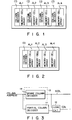
- Fig. 1 The pattern layout of the chip construction in the conventional DRAM is shown in Fig. 1. That is, memory cells are divided into four memory cell arrays AL1 to AL4 and a column decoder CD and a sense amplifier (not shown) are provided for each of the memory cell arrays AL1 to AL4.
- a recent DRAM includes a redundant circuit for remedying or compensating a defective chip by replacing defective memory cells of several bits to several thousand bits by spare memory cells which are preparatorily provided.
- the redundant circuit is a means for replacing a row line or a column line to which the defective memory cells are connected by a spare row line or spare column line provided in the same memory cell array in which the former row line or column line is provided in order to replace the defective memory cells by other memory cells which are provided as spare memory cells.
- a spare column decoder which has a group of fuse elements and in which a column address can be programmed by cutting off specified fuse elements is provided and a spare memory cell can be selected by selecting the spare column line by use of the spare column decoder without selecting the defective memory cell when a column address corresponding to the defective memory cell is input.
- a spare row decoder which has a group of fuse elements and in which a row address can be programmed by cutting off specified fuse elements is provided and a spare memory cell can be selected by selecting the spare row line by use of the spare row decoder without selecting the defective memory cell when a row address corresponding to the defective memory cell is input.
- Fig. 3 shows an example of the conventional column redundant circuit. That is, 11 denotes one of a plurality of partial column decoders provided in the column decoder CD, 12 denotes a logic circuit connected to the output side of the partial column decoder 11, and CDL denotes a column selection line supplied with a column selection signal via the logic circuit 12. Further, 13 denotes a column redundant circuit and SCDL denotes a spare column selection line supplied with a spare column selection signal from the column redundant circuit 13. A spare column line (not shown) to which spare memory cells (not shown) are connected is selected by a signal on the spare column selection line SCDL.
- the column redundant circuit 13 14 denotes a programmable column decoder (spare column decoder) having a fuse element group and receiving a column address.
- the spare column decoder 14 fuse elements are previously cut off so as to activate an output thereof if a defective memory cell is present and when a column address corresponding to the defective memory cell is input.
- the decoder output is supplied as a column selection signal to the column selection line CDL via the logic circuit 12.
- the decoder output from the spare column decoder 14 is set in the non-activated state.
- the decoder output of the spare column decoder 14 is set into the activated state and supplied as a spare column selection signal to the spare column selection line SCDL, and thus the defective memory cell is substantially replaced by a memory cell connected to the spare column selection line SCDL.
- an output generated at this time from the spare column decoder 14 is input to the logic circuit 12 to set the output (column selection signal) of the logic circuit 12 into the non-activated state.
- the maximum number of memory cells which can be remedied or compensated for by use of the above column redundant circuit is determined according to the number of spare memory cells.
- the number of memory cells which can be actually compensated for is largely dependent on the number of divided memory cell arrays, the number of column decoders, the number of column redundant circuits and the like.
- the column compensation rates in the chip constructions shown in Figs. 1 and 2 are compared with each other. In the chip construction shown in Fig.
- a defective column line can be replaced by a spare column line for each memory cell array even when a defective column line is present in each of the memory cell arrays if a column redundant circuit is provided for each of the column decoders of the respective memory cell arrays. That is, when a chip having four column decoders as shown in Fig. 1 is used, one defective column line can be compensated for for each column decoder and four defective column lines at maximum can be compensated for. In contrast, in the chip construction shown in Fig.
- a problem similar to the above problem occurs when a row redundant circuit is provided in the chip construction in which the integration density is increased by commonly selecting four or more memory cell arrays by use of a single row decoder.
- EP-A-0 333 207 shows a memory device in which two transistors are inserted in series between a main memory cell block and the sense amplifier and between the spare cell and sense amplifier, for selection of column, and selection of the spare cell. This shows read out time.
- an object of this invention is to provide a semiconductor memory device capable of enhancing the column compensation rate or row compensation rate while suppressing an increase in the chip area in a case where a column redundant circuit or row redundant circuit is provided in a chip construction in which the integration density is increased by commonly selecting four or more memory cell arrays by use of a single column decoder or row decoder.
- a semiconductor memory device comprising:
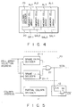
- Fig. 4 is a diagram schematically showing the pattern layout of a DRAM chip according to a first embodiment of this invention and having a redundant circuit provided therein.
- a chip construction in which column lines of four or more (four in this embodiment) memory cell arrays AL1 to AL4 are commonly selected by a column selection line supplied with a column selection signal output from a single column decoder to enhance the integration density is used.
- a column redundant circuit for selecting spare column lines (not shown) for defective memory cell compensation provided for the respective memory cell arrays AL1 to AL4 is provided.
- a memory cell array is divided into the four memory cell arrays AL1 to AL4, for example.
- a column decoder CD, a sense amplifier (not shown) and the like are arranged on one end side of the chip.
- the column decoder CD includes a plurality of partial column decoders commonly used for the four memory cell arrays AL1 to AL4.
- a column redundant circuit 20 is arranged in position adjacent to the column decoder CD on the one end side of the chip.
- the column redundant circuit 20 includes a spare column decoder constructed by a programmable address decoder having a fuse element group, and receives an address for memory cell array selection together with a column address and effects the decoding operation.
- the spare column line is selected by an output of the column redundant circuit 20.
- SAL1 to SAL4 respectively denote redundant memory cell groups provided in positions adjacent to the memory cell arrays AL1 to AL4, and the redundant memory cell groups SAL1 to SAL4 are connected to the spare column lines.
- memory cells for each of the four memory cell arrays can be remedied or compensated for by use of a single column redundant circuit 20, and the concrete construction is shown in Fig. 5.
- Fig. 5 shows one partial column decoder 11 and column redundant circuit 20 in the column decoder CD
- 12 denotes a logic circuit connected to the output side of the partial column decoder 11 and an output (column selection signal) of the logic circuit 12 is supplied to the column selection line CDL.
- An output (spare column selection signal) of the column redundant circuit 20 is supplied to one spare column selection line SCDL.
- the spare column selection line SCDL is provided to select the spare column lines.
- the column redundant circuit 20 includes four spare column decoders 21-1 to 21-4 of the same number as that of memory cell arrays which can be selected by the column selection line supplied with an output of the partial column decoder 11, and a logic circuit which is an OR gate 22 in this example and derives a logical sum of outputs of the four spare column decoders 21-1 to 21-4 and outputs the logical sum to the spare column selection line SCDL.
- An output of the OR gate 22 is supplied to the logic circuit 12.
- each of the spare column decoders 21-1 to 21-4 includes a fuse element group formed of polysilicon, for example, and receives an address for memory cell array selection, for example, 2-bit row address together with an n-bit column address and decodes the same. That is, in a case where a defective memory cell is present, specified fuse elements of the spare column decoders 21-1 to 21-4 are selectively cut off by use of a laser beam or the like so as to activate an output thereof when an address corresponding to the defective memory cell is input.
- the logic circuit 12 includes an inverter 15 for inverting an output of the OR gate 22, for example, and an AND gate 16 supplied with outputs of the inverter 15 and partial column decoder 11.
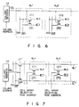
- a single-layered interconnection layer which becomes necessary because the column decoder CD commonly used for the four memory cell arrays AL1 to AL4 is collectively disposed in one place as shown in Fig. 4 can be used according to two circuit arrangements respectively shown in Figs. 6 and 7. That is, as shown in Fig. 6, in the first circuit arrangement, the additionally provided single-layered interconnection layer is assigned to the column selection line CDL extending from the output terminal of the column decoder CD and the column selection line CDL is commonly provided on the memory cell arrays AL1, AL2, --- to select column selection transistors CT1, /CT1, CT2, /CT2, ---.
- the column selection line CDL is provided in parallel with the column line pairs BL1, /BL1; BL2, /BL2; --- of the memory cell arrays AL1, AL2, ---.
- the additionally provided single-layered interconnection layer is assigned to the second column line pairs BL'', /BL'', --- and the second column line pairs BL'', /BL'', --- are commonly provided on the memory cell arrays AL1, AL2, --- and connected to one-side ends of first column selection transistors CT1, /CT1; CT2, /CT2, --- of the memory cell arrays AL1, AL2, --- and connected to one-side ends of second column selection transistors CT'', /CT'', ---.
- the other ends of the second column selection transistors CT'', /CT'', --- are commonly connected to common data line pair DQ'', /DQ'' and the column selection line CDL extending from the output terminal of the column decoder CD is used to select the second column selection transistors CT", /CT", ---.
- the first column selection transistors CT1, /CT1; CT2, /CT2; --- are selected by a memory cell array selection row address.
- the second paired column lines BL" and /BL" are provided in parallel with the first column line pairs BL1, /BL1; BL2, /BL2; --- of the memory cell arrays AL1, AL2, ---.
- one of the outputs of the spare column decoders 21-1 to 21-4 is set into the activated state and supplied as a spare column selection signal to the spare column selection line SCDL via the OR gate 22, thereby permitting the defective memory cell to be replaced by the memory cell connected to the spare column line.
- a signal lying on the spare column selection line SCDL at this time is input to the logic circuit 12 and the output (column selection signal) of the logic circuit 12 is set into the non-activated state.
- a single column redundant circuit 20 which can select a spare column line to be used instead of a defective memory cell to be compensated independently for each memory cell array by adding an address for selection for each memory cell array. Therefore, the same column remedying or compensating rate as in a case wherein the conventional column redundant circuit is provided for each column decoder of the memory cell array in a chip construction having a column decoder provided for each memory cell array as shown in Fig. 1 can be obtained and an increase in the chip area can be suppressed.
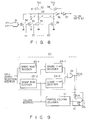
- Fig. 8 shows a concrete construction of a spare column decoder 21-1 which is one of the spare column decoders 21-1 to 21-4.
- a NAND gate 31 is supplied with X1 and X2 as memory cell array selection row addresses.
- the NAND gates 31 in the other spare column decoders 21-2 to 21-4 are respectively supplied with /X1 and X2, X1 and /X2, and /X1 and /X2.
- the source-drain path of a precharging P-channel MOS transistor 33 is connected between an application node of power source potential VCC and a node 32.
- the gate of the transistor 33 is supplied with a precharge control pulse signal ⁇ .
- the source-drain path of an N-channel MOS transistor 34 whose gate is connected to receive an output of the NAND gate 31 is connected between the node 32 and a ground potential terminal.
- fuse elements F and the respective source-drain paths of a plurality of N-channel MOS transistors35, 35, --- are series-connected between the node 32 and the ground potential terminal.
- the gates of the plurality of MOS transistors 35, 35, --- are respectively supplied with complementary data Y1 and /Y1, ---, Yn and /Yn of an n-bit column address.
- the node 32 is connected to an input terminal of an inverter 36.
- the output terminal of the inverter 36 is connected to an output terminal of an inverter 37.
- An output of the inverter 37 is supplied to the OR gate 22.
- the source-drain path of a P-channel MOS transistor 38 is connected between the application node of power source potential VCC and the node 32.
- the gate of the MOS transistor 38 is supplied with an output of the inverter 36.
- the spare column decoder 21-1 with the above construction, if a defective memory cell is present in a corresponding memory cell array AL1, one of the fuse elements F of each pair is cut off to program a column address for the defective memory cell. For example, when a Y1 bit of the column address corresponding to the defective memory cell is "1", the fuse element F which is series-connected with the MOS transistor 35 whose gate is connected to receive /Y1 is cut off.
- an output of the inverter 36 is set to the "L” level and an output of the inverter 37 is set to the "H” level, thereby driving the spare column selection line SCDL to the "H” level via the OR gate 22.
- the MOS transistor 38 has a function to maintain the potential of the node 32 at the "H” level even after the period of precharging by the MOS transistor 33 is terminated and the MOS transistor 33 is turned off.
- an output of the inverter 15 in the logic circuit 12 shown in Fig. 5 is set to the "L” level and an output of the AND gate 16 is also set to the "L” level so that the normal column selection line CDL will not be driven.
- Fig. 9 shows the construction of the redundant circuit 20 according to a second embodiment of this invention.
- the redundant circuit 20 includes two spare row decoders 23-1 and 23-2 for receiving a memory cell array selection address used for selection of each memory cell array and decoding the same, two spare column decoders 24-1 and 24-2 for receiving outputs of the spare row decoders together with the column address and decoding the same, and an OR gate 22 for deriving a logical sum of the outputs of the spare column decoders 24-1 and 24-2 and supplying the logical sum to the spare column selection line SCDL.
- Programmable fuse elements are provided in the spare column decoders 24-1 and 24-2. If a defective memory cell is present in the memory cell arrays AL1 to AL4, specified fuse elements in the spare row decoders 23-1 and 23-2 are previously cut off so as to activate the outputs thereof when an address necessary for selecting the memory cell array in which the defective memory cell is present is input. Likewise, fuse elements are provided in the spare column decoders 24-1 and 24-2, and specified fuse elements are previously cut off so as to activate the outputs thereof when the decoder outputs of the spare row decoders 23-1 and 23-2 are set in the selected state and a column address for the defective memory cell is input.
- the number of memory cell arrays selected by the spare row decoder 23-1 or 23-2 is not limited to one, and specified fuse elements may be cut off so as to decode the upper one bit or lower one bit of a 2-bit row address input to simultaneously select two memory cell arrays.
- the remedying or compensating operation for the defective memory cells of the two memory cell arrays can be commonly effected by use of the spare column decoder 24-1 or 24-2.
- the number of spare column decoders used can be reduced in comparison with the column redundant circuit shown in Fig. 5. That is, in the column redundant circuit shown in Fig. 5, four spare column decoders of the same number as that of memory cell arrays which can be selected by a column selection line to which an output of the column decoder is supplied are required, but in the column redundant circuit shown in Fig. 9, a desired number of spare column decoders which is not larger than the number of memory cell arrays can be used.
- Fig. 10 shows the concrete construction of the spare row decoder 23-1 and the spare column decoder 24-1 which are respectively used as one of the spare row decoders 23-1 and 23-2 and one of the spare column decoders 24-1 and 24-2 in the embodiment of Fig. 9.
- the construction of the spare column decoder 24-1 in this embodiment is equal to that obtained by removing the NAND gate 31 and the N-channel MOS transistor 34 from the spare column decoder shown in Fig. 8, and therefore, the explanation therefor is omitted.
- the spare column decoder 24-1 is constructed by four fuse elements F and N-channel MOS transistors 38.
- the four fuse elements F and the source-drain paths of the respective N-channel MOS transistors 38 are series-connected between the node 32 of the spare column decoder 24-1 and the ground potential terminal.
- the gates of the four MOS transistors 38, 38, --- are respectively supplied with 2-bit complementary row addresses X1 and /X1; and X2 and /X2 for memory cell array selection.
- the spare row decoder 23-1 four fuse elements F are selectively cut off to select two memory cell arrays AL1 and AL2, for example. Further, in the spare column decoder 24-1, the fuse elements F are selectively cut off to program a column address corresponding to a defective memory cell.
- Figs. 11 and 12 schematically show the pattern layouts of DRAM chips according to third and fourth embodiments of this invention, and like the former embodiments, this invention can be applied to these embodiments. That is, the pattern layout of Fig. 11 is different from the pattern layout of Fig. 4 in that a column decoder section 50 including a column decoder and a spare column decoder is disposed in the central portion of the pattern layout.
- pattern layout of Fig. 12 includes two pattern layouts which are the same as that shown in Fig. 11.
- the column redundant circuit is provided as the redundant circuit, but it is of course possible to use a row redundant circuit in substantially the same manner as in the above embodiments.
- the semiconductor memory device of this invention in a case where a column redundant circuit or row redundant circuit is provided in a chip construction in which the integration density is enhanced by using one column decoder or row decoder to commonly select a plurality of memory cell arrays, the column compensation rate or row compensation rate can be enhanced while an increase in the chip area is suppressed.
Landscapes
- For Increasing The Reliability Of Semiconductor Memories (AREA)
- Dram (AREA)
- Techniques For Improving Reliability Of Storages (AREA)
Claims (3)
- Dispositif de mémoire à semiconducteur comprenant :une pluralité de réseaux de cellules de mémoire (AL1 à AL4) ;une pluralité de lignes de sélection de colonne (CDL) prévues en commun pour ladite pluralité de réseaux de cellules de mémoire ;un circuit de sélection de ligne de sélection de colonne (CD) pour recevoir une adresse et pour sélectionner ladite pluralité de lignes de sélection de colonne conformément à l'adresse reçue ;une ligne de sélection de colonne de secours (SCDL) utilisée pour une compensation de cellule de mémoire défectueuse ; etun circuit redondant (20) dans lequel une adresse de sélection de colonne spécifiée correspondant à une ligne de sélection incluse dans ladite pluralité de lignes de sélection de colonne et associée à une cellule de mémoire défectueuse est programmable et qui est conçu pour recevoir une adresse de colonne et une adresse de sélection de réseau de cellules de mémoire pour sélectionner l'un de ladite pluralité de réseaux de cellules de mémoire, le circuit pouvant être activé pour sélectionner ladite ligne de sélection de colonne de secours conformément aux adresses reçues,caractérisé en ce que :ledit circuit redondant inclut des décodeurs de colonne de secours (21-1 à 21-4) selon le même nombre que celui desdits réseaux de cellules de mémoire, recevant une adresse de colonne et une adresse de sélection de réseau de cellules de mémoire et décodant celles-ci ; et un circuit logique (22) pour dériver une somme logique de sorties de ladite pluralité de décodeurs de colonne de secours et pour appliquer la somme logique sur ladite ligne de sélection de colonne de secours ; et en ce que :ledit circuit de sélection de ligne de sélection de colonne (CD) inclut un décodeur de colonne partiel où la sortie dudit décodeur de colonne partiel est commandée sur la base d'une sortie (SCDL) dudit circuit logique (22).
- Dispositif de mémoire à semiconducteur selon la revendication 1, caractérisé en ce que ledit circuit redondant inclut une pluralité de décodeurs de rangée de secours (23-1, 23-2) pour recevoir l'adresse de sélection de réseau de cellules de mémoire et pour décoder celle-ci ; dans lequel ladite pluralité de décodeurs de colonne de secours (24-1, 24-2) reçoivent des sorties de décodeur desdits décodeurs de rangée de secours et l'adresse de colonne pour décoder celle-ci.
- Dispositif de mémoire à semiconducteur selon la revendication 1, caractérisé en ce que lesdites lignes de sélection de colonne sont formées en commun sur ladite pluralité de réseaux de cellules de mémoire et sont agencées en parallèle avec des lignes de colonne desdits réseaux de cellules de mémoire pour sélectionner lesdites lignes de colonne.
Applications Claiming Priority (2)
| Application Number | Priority Date | Filing Date | Title |
|---|---|---|---|
| JP219937/90 | 1990-08-23 | ||
| JP2219937A JPH04103099A (ja) | 1990-08-23 | 1990-08-23 | 半導体記憶装置 |
Publications (3)
| Publication Number | Publication Date |
|---|---|
| EP0472209A2 EP0472209A2 (fr) | 1992-02-26 |
| EP0472209A3 EP0472209A3 (en) | 1992-12-23 |
| EP0472209B1 true EP0472209B1 (fr) | 1996-06-05 |
Family
ID=16743365
Family Applications (1)
| Application Number | Title | Priority Date | Filing Date |
|---|---|---|---|
| EP91114171A Expired - Lifetime EP0472209B1 (fr) | 1990-08-23 | 1991-08-23 | Dispositif de mémoire à semi-conducteur ayant un circuit de redondance |
Country Status (5)
| Country | Link |
|---|---|
| US (1) | US5272672A (fr) |
| EP (1) | EP0472209B1 (fr) |
| JP (1) | JPH04103099A (fr) |
| KR (1) | KR950013400B1 (fr) |
| DE (1) | DE69120000T2 (fr) |
Families Citing this family (18)
| Publication number | Priority date | Publication date | Assignee | Title |
|---|---|---|---|---|
| US5740114A (en) * | 1992-03-23 | 1998-04-14 | Matsushita Electric Industrial Co., Ltd. | Redundant memory cell selecting circuit having fuses coupled to memory cell group address and memory cell block address |
| JPH0696598A (ja) * | 1992-07-10 | 1994-04-08 | Texas Instr Japan Ltd | 半導体メモリ装置及び欠陥メモリセル救済回路 |
| US5469401A (en) * | 1992-07-14 | 1995-11-21 | Mosaid Technologies Incorporated | Column redundancy scheme for DRAM using normal and redundant column decoders programmed with defective array address and defective column address |
| JP2981346B2 (ja) * | 1992-08-31 | 1999-11-22 | シャープ株式会社 | 読み出し専用半導体記憶装置 |
| EP0612074B1 (fr) * | 1993-02-19 | 2001-05-02 | Infineon Technologies AG | Dispositif de colonnes redondantes pour une mémoire |
| DE69319886T2 (de) * | 1993-03-31 | 1999-03-18 | Sgs Thomson Microelectronics | Halbleiterspeicher mit Speichermatrix, der mit einem einzigen Sektor assoziierte Redundantezellenspalte enthält |
| JP2856645B2 (ja) * | 1993-09-13 | 1999-02-10 | 株式会社東芝 | 半導体記憶装置 |
| DE69412230T2 (de) * | 1994-02-17 | 1999-04-08 | Sgs Thomson Microelectronics | Verfahren zur Programmierung von Redundanzregistern in einer Spaltenredundanzschaltung für einen Halbleiterspeicherbaustein |
| ATE187826T1 (de) * | 1994-08-12 | 2000-01-15 | Siemens Ag | Redundanz-schaltungsanordnung für einen integrierten halbleiterspeicher |
| GB2292236A (en) * | 1995-04-04 | 1996-02-14 | Memory Corp Plc | Improved partial memory engine |
| JP3230795B2 (ja) * | 1995-09-29 | 2001-11-19 | シャープ株式会社 | 読み出し専用半導体記憶装置 |
| US5821772A (en) * | 1996-08-07 | 1998-10-13 | Xilinx, Inc. | Programmable address decoder for programmable logic device |
| US6137307A (en) * | 1998-08-04 | 2000-10-24 | Xilinx, Inc. | Structure and method for loading wide frames of data from a narrow input bus |
| US6097210A (en) * | 1998-08-04 | 2000-08-01 | Xilinx, Inc. | Multiplexer array with shifted input traces |
| US6069489A (en) * | 1998-08-04 | 2000-05-30 | Xilinx, Inc. | FPGA having fast configuration memory data readback |
| KR20030000766A (ko) * | 2001-06-27 | 2003-01-06 | 삼성전자 주식회사 | 반도체 메모리의 리던던시 회로 |
| KR100498598B1 (ko) * | 2003-04-30 | 2005-07-01 | 주식회사 하이닉스반도체 | 리페어 효율을 향상시킨 반도체 메모리 장치 |
| US7093989B2 (en) * | 2004-05-27 | 2006-08-22 | Silverbrook Research Pty Ltd | Printer comprising two uneven printhead modules and at least two printer controllers, one which spends print data to the other |
Family Cites Families (8)
| Publication number | Priority date | Publication date | Assignee | Title |
|---|---|---|---|---|
| JPS6376191A (ja) * | 1986-09-19 | 1988-04-06 | Hitachi Ltd | 半導体記憶装置 |
| JPH0748315B2 (ja) * | 1986-12-22 | 1995-05-24 | 三菱電機株式会社 | 半導体記憶装置 |
| JP2629697B2 (ja) * | 1987-03-27 | 1997-07-09 | 日本電気株式会社 | 半導体記憶装置 |
| JPH01119995A (ja) * | 1987-11-02 | 1989-05-12 | Toshiba Corp | 半導体メモリ |
| JP2618938B2 (ja) * | 1987-11-25 | 1997-06-11 | 株式会社東芝 | 半導体記憶装置 |
| EP0333207B1 (fr) * | 1988-03-18 | 1997-06-11 | Kabushiki Kaisha Toshiba | Mémoire ROM masquée avec des cellules mémoire de remplacement |
| NL8900026A (nl) * | 1989-01-06 | 1990-08-01 | Philips Nv | Matrixgeheugen, bevattende standaardblokken, standaardsubblokken, een redundant blok, en redundante subblokken, alsmede geintegreerde schakeling bevattende meerdere van zulke matrixgeheugens. |
| JPH0748314B2 (ja) * | 1989-02-02 | 1995-05-24 | 株式会社東芝 | 半導体記憶装置 |
-
1990
- 1990-08-23 JP JP2219937A patent/JPH04103099A/ja active Pending
-
1991
- 1991-08-20 KR KR1019910014297A patent/KR950013400B1/ko not_active IP Right Cessation
- 1991-08-22 US US07/748,518 patent/US5272672A/en not_active Expired - Lifetime
- 1991-08-23 DE DE69120000T patent/DE69120000T2/de not_active Expired - Lifetime
- 1991-08-23 EP EP91114171A patent/EP0472209B1/fr not_active Expired - Lifetime
Also Published As
| Publication number | Publication date |
|---|---|
| US5272672A (en) | 1993-12-21 |
| KR920005174A (ko) | 1992-03-28 |
| JPH04103099A (ja) | 1992-04-06 |
| DE69120000T2 (de) | 1996-11-28 |
| KR950013400B1 (ko) | 1995-11-08 |
| EP0472209A3 (en) | 1992-12-23 |
| DE69120000D1 (de) | 1996-07-11 |
| EP0472209A2 (fr) | 1992-02-26 |
Similar Documents
| Publication | Publication Date | Title |
|---|---|---|
| EP0472209B1 (fr) | Dispositif de mémoire à semi-conducteur ayant un circuit de redondance | |
| US5349556A (en) | Row redundancy circuit sharing a fuse box | |
| US5124948A (en) | Mask ROM with spare memory cells | |
| KR950004872B1 (ko) | 정규 메모리 셀 어레이와 동시에 억세스가능한 용장 메모리 셀 컬럼을 갖고 있는 반도체 메모리 디바이스 | |
| US4837747A (en) | Redundary circuit with a spare main decoder responsive to an address of a defective cell in a selected cell block | |
| US7106643B2 (en) | Method for manufacturing memory device provided with a defect recovery mechanism featuring a redundancy circuit | |
| KR950004623B1 (ko) | 리던던시 효율이 향상되는 반도체 메모리 장치 | |
| US6172916B1 (en) | Semiconductor memory device having a large band width and allowing efficient execution of redundant repair | |
| US4648075A (en) | Redundancy circuit for a semiconductor memory device | |
| US5485424A (en) | Semiconductor memory and redundant-address writing method | |
| EP0410413B1 (fr) | Dispositif de mémoire à semiconducteur à réseau de cellules de mémoire de réserve | |
| US5555522A (en) | Semiconductor memory having redundant cells | |
| US5446692A (en) | Semiconductor memory device having redundancy memory cells shared among memory blocks | |
| US6144591A (en) | Redundancy selection circuit for semiconductor memories | |
| US5434814A (en) | Circuit for repairing defective read only memories with redundant NAND string | |
| EP0503100B1 (fr) | Memoire a semi-conducteur | |
| US5357470A (en) | Semiconductor memory device having redundancy memory cells | |
| JP2629463B2 (ja) | 半導体記憶回路 | |
| KR0140350B1 (ko) | 반도체 기억 장치 | |
| US5390150A (en) | Semiconductor memory device with redundancy structure suppressing power consumption | |
| US6335897B1 (en) | Semiconductor memory device including redundancy circuit adopting latch cell | |
| JPH04222998A (ja) | 半導体メモリ装置 | |
| US5877992A (en) | Data-bit redundancy in semiconductor memories | |
| US6288964B1 (en) | Method to electrically program antifuses | |
| US5479371A (en) | Semiconductor memory device |
Legal Events
| Date | Code | Title | Description |
|---|---|---|---|
| PUAI | Public reference made under article 153(3) epc to a published international application that has entered the european phase |
Free format text: ORIGINAL CODE: 0009012 |
|
| 17P | Request for examination filed |
Effective date: 19910823 |
|
| AK | Designated contracting states |
Kind code of ref document: A2 Designated state(s): DE FR GB |
|
| PUAL | Search report despatched |
Free format text: ORIGINAL CODE: 0009013 |
|
| AK | Designated contracting states |
Kind code of ref document: A3 Designated state(s): DE FR GB |
|
| 17Q | First examination report despatched |
Effective date: 19940526 |
|
| GRAH | Despatch of communication of intention to grant a patent |
Free format text: ORIGINAL CODE: EPIDOS IGRA |
|
| GRAA | (expected) grant |
Free format text: ORIGINAL CODE: 0009210 |
|
| AK | Designated contracting states |
Kind code of ref document: B1 Designated state(s): DE FR GB |
|
| REF | Corresponds to: |
Ref document number: 69120000 Country of ref document: DE Date of ref document: 19960711 |
|
| ET | Fr: translation filed | ||
| PLBE | No opposition filed within time limit |
Free format text: ORIGINAL CODE: 0009261 |
|
| STAA | Information on the status of an ep patent application or granted ep patent |
Free format text: STATUS: NO OPPOSITION FILED WITHIN TIME LIMIT |
|
| 26N | No opposition filed | ||
| REG | Reference to a national code |
Ref country code: GB Ref legal event code: IF02 |
|
| PGFP | Annual fee paid to national office [announced via postgrant information from national office to epo] |
Ref country code: FR Payment date: 20100824 Year of fee payment: 20 Ref country code: DE Payment date: 20100818 Year of fee payment: 20 |
|
| PGFP | Annual fee paid to national office [announced via postgrant information from national office to epo] |
Ref country code: GB Payment date: 20100818 Year of fee payment: 20 |
|
| REG | Reference to a national code |
Ref country code: DE Ref legal event code: R071 Ref document number: 69120000 Country of ref document: DE |
|
| REG | Reference to a national code |
Ref country code: DE Ref legal event code: R071 Ref document number: 69120000 Country of ref document: DE |
|
| PG25 | Lapsed in a contracting state [announced via postgrant information from national office to epo] |
Ref country code: GB Free format text: LAPSE BECAUSE OF EXPIRATION OF PROTECTION Effective date: 20110822 |
|
| PG25 | Lapsed in a contracting state [announced via postgrant information from national office to epo] |
Ref country code: DE Free format text: LAPSE BECAUSE OF EXPIRATION OF PROTECTION Effective date: 20110824 |