EP0464794A2 - Système de génération de motif peint et méthode de peinture de motif utilisant le système - Google Patents
Système de génération de motif peint et méthode de peinture de motif utilisant le système Download PDFInfo
- Publication number
- EP0464794A2 EP0464794A2 EP91111032A EP91111032A EP0464794A2 EP 0464794 A2 EP0464794 A2 EP 0464794A2 EP 91111032 A EP91111032 A EP 91111032A EP 91111032 A EP91111032 A EP 91111032A EP 0464794 A2 EP0464794 A2 EP 0464794A2
- Authority
- EP
- European Patent Office
- Prior art keywords
- data
- outline
- pattern
- memory
- painting
- Prior art date
- Legal status (The legal status is an assumption and is not a legal conclusion. Google has not performed a legal analysis and makes no representation as to the accuracy of the status listed.)
- Granted
Links
- 238000010422 painting Methods 0.000 title claims abstract description 66
- 238000000034 method Methods 0.000 title claims abstract description 17
- 230000015654 memory Effects 0.000 claims abstract description 98
- 239000003973 paint Substances 0.000 claims description 3
- 238000010586 diagram Methods 0.000 description 10
- 230000008569 process Effects 0.000 description 4
- 230000006870 function Effects 0.000 description 1
- 230000004048 modification Effects 0.000 description 1
- 238000012986 modification Methods 0.000 description 1
- 230000009467 reduction Effects 0.000 description 1
Images


Classifications
-
- H—ELECTRICITY
- H01—ELECTRIC ELEMENTS
- H01L—SEMICONDUCTOR DEVICES NOT COVERED BY CLASS H10
- H01L29/00—Semiconductor devices adapted for rectifying, amplifying, oscillating or switching, or capacitors or resistors with at least one potential-jump barrier or surface barrier, e.g. PN junction depletion layer or carrier concentration layer; Details of semiconductor bodies or of electrodes thereof ; Multistep manufacturing processes therefor
-
- G—PHYSICS
- G06—COMPUTING; CALCULATING OR COUNTING
- G06T—IMAGE DATA PROCESSING OR GENERATION, IN GENERAL
- G06T11/00—2D [Two Dimensional] image generation
- G06T11/40—Filling a planar surface by adding surface attributes, e.g. colour or texture
-
- H—ELECTRICITY
- H01—ELECTRIC ELEMENTS
- H01L—SEMICONDUCTOR DEVICES NOT COVERED BY CLASS H10
- H01L21/00—Processes or apparatus adapted for the manufacture or treatment of semiconductor or solid state devices or of parts thereof
- H01L21/02—Manufacture or treatment of semiconductor devices or of parts thereof
- H01L21/027—Making masks on semiconductor bodies for further photolithographic processing not provided for in group H01L21/18 or H01L21/34
Definitions
- This invention relates to a painting pattern generation system for painting a plurality of regions enclosed by outlines (or boundaries) and a pattern painting method using the system.
- a painting method is commonly known by which a plurality of pattern interior areas enclosed only by outlines (or boundaries) are selectively painted based on an even-odd rule.
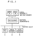
- Fig. 1 is a block diagram of a painting pattern generation system which uses the even-odd method.
- the system comprises a local memory (or a bit-map memory) 11 including a first memory area and a second memory area A and B, each size of which is matched to the size of a pattern to be generated, a pattern generating device 9 by which the contents of the first and the second memories are read out and then processed by a logical operation to generate a pattern, a central processing unit CPU 1 as a host CPU (or a processor) which can control the operation of the pattern generating device 9, and a main memory 3 and a font memory 5 connected to the host CPU 1.
- a local memory or a bit-map memory
- a and B each size of which is matched to the size of a pattern to be generated
- a pattern generating device 9 by which the contents of the first and the second memories are read out and then processed by a logical operation to generate a pattern
- a central processing unit CPU 1 as a host CPU (or a processor
- a white and a black pattern are expressed by two data units, "1" and "0".
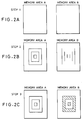
- a step 1 as shown in Fig. 2A the contents of the first and the second memories are initialized by the pattern generating device 9 under the control of the host CPU 1.
- the pattern generating device 9 draws outline data in the first memory A and provides a flag data in the second memory B.
- the flag data is required for a painting operation and generated by a predetermined rule.
- the pattern generating device 9 reads out the outline data and the flag data in the first and the second memories A and B, then calculates an exclusive OR (XOR) operation between two adjacent items of flag data along a scan line direction, which is a painting operation for the interior of an area enclosed by the outlines.
- XOR exclusive OR
- a logical OR operation between the result of the XOR operation and the outline data in the first memory A is carried out in the scan line direction.
- This OR operation is a compensation operation for the painting operation.
- the steps 1 to 3 are carried out for all scan lines on the outlines (or the closed curves which are generated by the outline data) involved in the pattern to obtain the completely painted pattern data.
- the completely painted pattern data is read out to the main memory 3 by the host CPU 1.
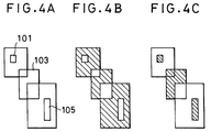
- the resultant pattern data is required as shown in Fig. 4B.
- the resultant pattern as shown in Fig. 4C is required by using the conventional pattern generation system, it is possible to generate the pattern with many processes. But the processes requires much time and must be executed under the control of a host CPU. Each process can process only one segment which means a closed pattern).
- the pattern generating device 9 draws outline data and flag data for segments 101 and 105 shown in Fig. 4A in the first and the second memories A and B which have already been initialized completely under the control of the host CPU 1. Then, the outline data and the painted pattern data is stored in the first and the second memories A and B, respectively, after completion of these painting operations.
- the host CPU 1 reads out the painted pattern data in the second memory B to be transferred to the main memory 3.
- the pattern generating device 9 initializes the contents of the first and the second memories A and B, then draws the outline data and the flag data of the segment 103 shown in Fig. 4A in the first and the second memories A and B as the painting operation.
- the painted pattern data in the second memory B is transferred to the main memory 3 in the host CPU 1 as in the step 1.
- a logical OR operation between the painted data transferred from the second memory 3 and the painted data which have been transferred in the step 1 shown in Fig. 5A is performed, then the resultant data is stored in the main memory 3.
- the pattern generating device 9 initializes completely the contents of the first and the second memories A and B, then draws the outline from the outline data and the flag data of all of the segments as shown in Fig. 4A in the first and the second memories A and B.
- the painting operation is not performed because there is no data to be painted. Accordingly, only the outline data in the first memory A is transferred to the main memory 3 in the host CPU 1. Then, the logical OR operation of the outline data and the data which has been stored in the step 2 is executed, and the result of the operation is transferred to the main memory 3 under the control of the host CPU 1.
- the required data such as the data shown in Fig. 4C can be stored in the main memory 3.
- the painting operations described above require much time to obtain the required pattern data because these painting operations must access the host CPU 1 more frequently.
- This invention is provided to overcome the problem of the conventional painting operations and the conventional pattern generation system in the prior art.
- An object of the present invention is therefore to provide a painting pattern generation system which can be made up of reduced hardware components, and which is capable of executing painting operations at a high speed.
- a painting pattern generation system for painting interior areas enclosed by outlines by using outline data and flag data, comprising: a first memory means used for storing data for drawing an outline by which patterns in the interior areas enclosed by the outline data are generated; a second memory means used for storing drawing flag data by which the interior areas are painted; an operational means for reading out the outline data and the flag data stored in the first and the second memory means, for performing an exclusive OR (XOR) operation between two adjacent items of flag data in the second memory means in a predetermined scan line direction, and for performing predetermined logical operations between the result of the XOR operation and the outline data in the first memory means in the scan line direction for all the scan lines to obtain the data for painting the patterns in the interior areas enclosed by the outline, and a writing means for writing the data for the pattern painted by the operation means into the first memory means and for further overlapping the data for the a next outline on the painted pattern data in the first memory means.
- XOR exclusive OR
- a pattern painting method for obtaining patterns painted in interior areas enclosed by the outline based on outline data comprising:
- the number of times the host CPU is accessed can be reduced by the system and the method based on the even-odd rule according to the present invention because a memory in the host CPU (which must be used frequently to generate the required painted patterns in the prior art) is not used to generate the required painted patterns.
- Fig. 6 is a block diagram of a painting pattern generating device which is capable of efficiently executing a painting operation for various patterns.
- the configuration of the painting pattern generating device is similar to that of the conventional painting pattern generating device as shown in Fig. 1, the functions of a host CPU 20 and a pattern generation system are different from those of the conventional painting pattern generation system.
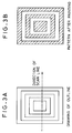
- the patterns as shown in Fig. 4C are used as patterns to be painted in the following description.
- the pattern generator 21 receives the clear command transferred from the CPU 20 for initializing the contents of the memories, then clears the contents of the first and the second memory regions A and B.
- the pattern generator 21 which has received the clear command from the host CPU 20 draws outlines for the segments 101 and 105 shown in Fig. 7A in the first and the second memory regions.
- the pattern generator 21 reads out the painting data stored in the first and the second memory regions, then performs an exclusive OR (XOR) operation between two adjacent items of flag data in the scan line direction (for painting the interior portion enclosed by the outline), and further performs a logical OR operation between the result of the XOR operation and the outline data from the first memory region A (for a compensation of data for painting the patterns in the interior areas).
- XOR exclusive OR
- the flag data in the second memory region is cleared after the operation for the scan line in the painting operation described above.
- the painting operation described above are operated along the scan lines for all closed curves (outlines), so that the painted pattern data of the segments 101 and 105 are obtained in the first memory region A shown in Fig. 7A.
- Fig. 8 is a block diagram of a calculator 22 for performing the XOR and OR operations which is widely used in the prior art for executing the painting operation described above.
- the pattern generator 21 which has received the drawing command transferred from the host CPU 20 overlaps the outline data for the segment 103 shown in Fig. 4A on the pattern data obtained in the step 1 described above, then further draws the flag data for the segment 103 in the second memory region B from the flags.
- the pattern generator 21 which has received the command for painting from the host CPU also performs the painting operation described in the step 1, then writes the result of the operation on the scan line in the memory region A and clears the flag data in the memory region B when the operation on the scan line is completed.
- the painting operations are executed for all of the scan lines on the closed curves to obtain the data for painting the pattern in the segments 101, 103, and 105.
- the pattern generator 21 which has received the outline drawing command from the host CPU 20 draws the outline data of all of the segments on the pattern painted in the segments 101, 103, and 105 in the first memory region A.
- the data for the pattern painted as shown in Fig. 4C can be obtained from the first memory region A.
- the host CPU 20 transfers the pattern data contained in the first memory region A by a block transfer command.
- the painting operation for a plurality of areas enclosed by closed curves (or outlines) can be executed with a reduction in the number of access items of a main memory.
- any element in a pattern can be divided and overlaps with another pattern by using two memory regions for painting.
Applications Claiming Priority (3)
| Application Number | Priority Date | Filing Date | Title |
|---|---|---|---|
| JP174374/90 | 1990-07-03 | ||
| JP2174374A JP2982973B2 (ja) | 1990-07-03 | 1990-07-03 | パターン塗り潰し方法 |
| JP17437490 | 1990-07-03 |
Publications (3)
| Publication Number | Publication Date |
|---|---|
| EP0464794A2 true EP0464794A2 (fr) | 1992-01-08 |
| EP0464794A3 EP0464794A3 (en) | 1993-06-16 |
| EP0464794B1 EP0464794B1 (fr) | 2001-10-10 |
Family
ID=15977499
Family Applications (1)
| Application Number | Title | Priority Date | Filing Date |
|---|---|---|---|
| EP91111032A Expired - Lifetime EP0464794B1 (fr) | 1990-07-03 | 1991-07-03 | Système de génération de motif peint et méthode de peinture de motif utilisant le système |
Country Status (5)
| Country | Link |
|---|---|
| US (1) | US5386502A (fr) |
| EP (1) | EP0464794B1 (fr) |
| JP (1) | JP2982973B2 (fr) |
| KR (1) | KR950006476B1 (fr) |
| DE (1) | DE69132756T2 (fr) |
Families Citing this family (7)
| Publication number | Priority date | Publication date | Assignee | Title |
|---|---|---|---|---|
| JP3332165B2 (ja) * | 1992-08-08 | 2002-10-07 | 株式会社リコー | 画像処理装置 |
| US5600768A (en) * | 1995-06-06 | 1997-02-04 | Apple Computer, Inc. | Image generation with dynamically consolidated list of image data |
| US5671345A (en) * | 1995-06-06 | 1997-09-23 | Apple Computer, Inc. | System and method for intercepting and reconstructing graphics management tool marking instructions |
| JP4100945B2 (ja) * | 2002-03-27 | 2008-06-11 | 富士通株式会社 | 図形描画装置 |
| US7030881B2 (en) * | 2003-03-25 | 2006-04-18 | Mitsubishi Electric Research Laboratories, Inc. | Method for converting two-dimensional objects to distance fields |
| US7106332B2 (en) * | 2003-03-25 | 2006-09-12 | Mitsubishi Electric Research Laboratories, Inc. | Method for converting two-dimensional pen strokes to distance fields |
| US20060103857A1 (en) * | 2004-11-17 | 2006-05-18 | Lexmark International, Inc. | Method of reducing a consumption of imaging substance when forming an image |
Citations (1)
| Publication number | Priority date | Publication date | Assignee | Title |
|---|---|---|---|---|
| US4745575A (en) * | 1983-12-22 | 1988-05-17 | International Business Machines Corporation | Area filling hardware for a color graphics frame buffer |
Family Cites Families (7)
| Publication number | Priority date | Publication date | Assignee | Title |
|---|---|---|---|---|
| DE2641708C3 (de) * | 1976-09-16 | 1980-02-21 | Paul 6456 Langenselbold Gutermuth | Unterdecke, insbesondere für gewerbliche Küchen, Schlachthauser, Waschkuchen u.dgl |
| JPS63135461U (fr) * | 1987-02-23 | 1988-09-06 | ||
| JPH01100590A (ja) * | 1987-10-13 | 1989-04-18 | Fujitsu Ltd | 表示制御方式 |
| CA1317041C (fr) * | 1987-12-24 | 1993-04-27 | Ncr Corporation | Dispositif creant un curseur au moyen de bandes reliees aux lignes de balayage individuelles |
| JPH01196675A (ja) * | 1988-01-30 | 1989-08-08 | Toshiba Corp | パターンデータ生成方式 |
| JPH0736163B2 (ja) * | 1988-08-26 | 1995-04-19 | 株式会社東芝 | 塗潰しパターン発生装置 |
| US4982343A (en) * | 1988-10-11 | 1991-01-01 | Next, Inc. | Method and apparatus for displaying a plurality of graphic images |
-
1990
- 1990-07-03 JP JP2174374A patent/JP2982973B2/ja not_active Expired - Fee Related
-
1991
- 1991-07-03 DE DE69132756T patent/DE69132756T2/de not_active Expired - Fee Related
- 1991-07-03 KR KR1019910011231A patent/KR950006476B1/ko not_active IP Right Cessation
- 1991-07-03 EP EP91111032A patent/EP0464794B1/fr not_active Expired - Lifetime
-
1993
- 1993-09-09 US US08/123,849 patent/US5386502A/en not_active Expired - Lifetime
Patent Citations (1)
| Publication number | Priority date | Publication date | Assignee | Title |
|---|---|---|---|---|
| US4745575A (en) * | 1983-12-22 | 1988-05-17 | International Business Machines Corporation | Area filling hardware for a color graphics frame buffer |
Non-Patent Citations (1)
| Title |
|---|
| IEEE TRANSACTIONS ON COMPUTERS vol. C-30, no. 1, January 1981, NY,USA pages 41 - 48 ACKLAND AND WESTE 'the edge flag algorithm- a fill method for raster scan displays' * |
Also Published As
| Publication number | Publication date |
|---|---|
| DE69132756T2 (de) | 2002-06-20 |
| JP2982973B2 (ja) | 1999-11-29 |
| KR920003543A (ko) | 1992-02-29 |
| KR950006476B1 (ko) | 1995-06-15 |
| DE69132756D1 (de) | 2001-11-15 |
| US5386502A (en) | 1995-01-31 |
| EP0464794B1 (fr) | 2001-10-10 |
| EP0464794A3 (en) | 1993-06-16 |
| JPH0464182A (ja) | 1992-02-28 |
Similar Documents
| Publication | Publication Date | Title |
|---|---|---|
| EP0327003B1 (fr) | Système de génération de données de configuration | |
| US5091976A (en) | Image coding method for extracting, segmenting, and coding image contours | |
| US5386510A (en) | Method of and apparatus for converting outline data to raster data | |
| JPS63198174A (ja) | 図形処理装置 | |
| EP0344686B1 (fr) | Procédé et processeur de découpage | |
| EP0464794A2 (fr) | Système de génération de motif peint et méthode de peinture de motif utilisant le système | |
| KR940006918B1 (ko) | 디지탈 활자체의 문자윤곽을 채우는 방법 및 시스템 | |
| KR100212412B1 (ko) | 문자패턴 생성장치 | |
| JP2634851B2 (ja) | 画像処理装置 | |
| US5526474A (en) | Image drawing with improved process for area ratio of pixel | |
| JP2770582B2 (ja) | 図形塗潰し装置 | |
| US6504543B1 (en) | Polygon drawing method and polygon drawing apparatus | |
| US5428719A (en) | Method and apparatus for generating high-quality pattern in accordance with an edge defining a character pattern | |
| JP2836617B2 (ja) | レンダリングプロセッサ | |
| KR970003326B1 (ko) | 문자 도형 발생 회로 | |
| JP2838556B2 (ja) | 画像処理装置 | |
| JP2835056B2 (ja) | 高品質文字パターン発生方式 | |
| JPH0486961A (ja) | 塗りつぶしパターン発生装置および発生方法 | |
| JPH0259871A (ja) | 画像処理装置および画像処理方法 | |
| JPS6316787B2 (fr) | ||
| JPS6282476A (ja) | 図形処理装置 | |
| JPH011075A (ja) | 画像処理装置 | |
| JPS60245085A (ja) | 塗潰し処理方式 | |
| JPS6376086A (ja) | 輪郭ベクトルからのパタ−ン復元方式 | |
| JPH11198465A (ja) | 文字出力装置 |
Legal Events
| Date | Code | Title | Description |
|---|---|---|---|
| PUAI | Public reference made under article 153(3) epc to a published international application that has entered the european phase |
Free format text: ORIGINAL CODE: 0009012 |
|
| 17P | Request for examination filed |
Effective date: 19910703 |
|
| AK | Designated contracting states |
Kind code of ref document: A2 Designated state(s): DE FR GB |
|
| PUAL | Search report despatched |
Free format text: ORIGINAL CODE: 0009013 |
|
| AK | Designated contracting states |
Kind code of ref document: A3 Designated state(s): DE FR GB |
|
| 17Q | First examination report despatched |
Effective date: 19970627 |
|
| GRAG | Despatch of communication of intention to grant |
Free format text: ORIGINAL CODE: EPIDOS AGRA |
|
| RIC1 | Information provided on ipc code assigned before grant |
Free format text: 7G 06T 11/40 A |
|
| GRAG | Despatch of communication of intention to grant |
Free format text: ORIGINAL CODE: EPIDOS AGRA |
|
| GRAH | Despatch of communication of intention to grant a patent |
Free format text: ORIGINAL CODE: EPIDOS IGRA |
|
| GRAH | Despatch of communication of intention to grant a patent |
Free format text: ORIGINAL CODE: EPIDOS IGRA |
|
| GRAA | (expected) grant |
Free format text: ORIGINAL CODE: 0009210 |
|
| AK | Designated contracting states |
Kind code of ref document: B1 Designated state(s): DE FR GB |
|
| REF | Corresponds to: |
Ref document number: 69132756 Country of ref document: DE Date of ref document: 20011115 |
|
| REG | Reference to a national code |
Ref country code: GB Ref legal event code: IF02 |
|
| ET | Fr: translation filed | ||
| PLBE | No opposition filed within time limit |
Free format text: ORIGINAL CODE: 0009261 |
|
| STAA | Information on the status of an ep patent application or granted ep patent |
Free format text: STATUS: NO OPPOSITION FILED WITHIN TIME LIMIT |
|
| 26N | No opposition filed | ||
| PGFP | Annual fee paid to national office [announced via postgrant information from national office to epo] |
Ref country code: GB Payment date: 20060628 Year of fee payment: 16 |
|
| PGFP | Annual fee paid to national office [announced via postgrant information from national office to epo] |
Ref country code: DE Payment date: 20060629 Year of fee payment: 16 |
|
| PGFP | Annual fee paid to national office [announced via postgrant information from national office to epo] |
Ref country code: FR Payment date: 20060719 Year of fee payment: 16 |
|
| GBPC | Gb: european patent ceased through non-payment of renewal fee |
Effective date: 20070703 |
|
| PG25 | Lapsed in a contracting state [announced via postgrant information from national office to epo] |
Ref country code: DE Free format text: LAPSE BECAUSE OF NON-PAYMENT OF DUE FEES Effective date: 20080201 |
|
| PG25 | Lapsed in a contracting state [announced via postgrant information from national office to epo] |
Ref country code: GB Free format text: LAPSE BECAUSE OF NON-PAYMENT OF DUE FEES Effective date: 20070703 |
|
| REG | Reference to a national code |
Ref country code: FR Ref legal event code: ST Effective date: 20080331 |
|
| PG25 | Lapsed in a contracting state [announced via postgrant information from national office to epo] |
Ref country code: FR Free format text: LAPSE BECAUSE OF NON-PAYMENT OF DUE FEES Effective date: 20070731 |