EP0457591A2 - Halbleiterspeicheranordnung mit reduzierten parasitären Kapazitäten zwischen Bitleitungen - Google Patents
Halbleiterspeicheranordnung mit reduzierten parasitären Kapazitäten zwischen Bitleitungen Download PDFInfo
- Publication number
- EP0457591A2 EP0457591A2 EP91304409A EP91304409A EP0457591A2 EP 0457591 A2 EP0457591 A2 EP 0457591A2 EP 91304409 A EP91304409 A EP 91304409A EP 91304409 A EP91304409 A EP 91304409A EP 0457591 A2 EP0457591 A2 EP 0457591A2
- Authority
- EP
- European Patent Office
- Prior art keywords
- bit lines
- sense amplifiers
- conductive shield
- shield plate
- plate
- Prior art date
- Legal status (The legal status is an assumption and is not a legal conclusion. Google has not performed a legal analysis and makes no representation as to the accuracy of the status listed.)
- Granted
Links
Images


Classifications
-
- G—PHYSICS
- G11—INFORMATION STORAGE
- G11C—STATIC STORES
- G11C7/00—Arrangements for writing information into, or reading information out from, a digital store
- G11C7/18—Bit line organisation; Bit line lay-out
-
- G—PHYSICS
- G11—INFORMATION STORAGE
- G11C—STATIC STORES
- G11C11/00—Digital stores characterised by the use of particular electric or magnetic storage elements; Storage elements therefor
- G11C11/21—Digital stores characterised by the use of particular electric or magnetic storage elements; Storage elements therefor using electric elements
- G11C11/34—Digital stores characterised by the use of particular electric or magnetic storage elements; Storage elements therefor using electric elements using semiconductor devices
- G11C11/40—Digital stores characterised by the use of particular electric or magnetic storage elements; Storage elements therefor using electric elements using semiconductor devices using transistors
- G11C11/401—Digital stores characterised by the use of particular electric or magnetic storage elements; Storage elements therefor using electric elements using semiconductor devices using transistors forming cells needing refreshing or charge regeneration, i.e. dynamic cells
- G11C11/4063—Auxiliary circuits, e.g. for addressing, decoding, driving, writing, sensing or timing
- G11C11/407—Auxiliary circuits, e.g. for addressing, decoding, driving, writing, sensing or timing for memory cells of the field-effect type
- G11C11/409—Read-write [R-W] circuits
- G11C11/4097—Bit-line organisation, e.g. bit-line layout, folded bit lines
Definitions
- the present invention relates to a semiconductor memory device, and more particularly, to a dynamic MOS (metal-oxide-semiconductor, broadly MIS) random access memory (RAM) having a highly-integrated configuration.
- MOS metal-oxide-semiconductor, broadly MIS
- RAM random access memory
- bit lines are first formed on a cell transistor portion, and then a capacitor electrode portion (cell plate electrode) is formed over the bit lines, so that a capacitor is created on the bit lines.
- the cell plate electrode serves as a conductive shield plate for the bit lines, to thereby reduce the parasitic electrostatic capacity between the bit lines.
- This stacked capacitor cell configuration has not been applied to the bit lines inside of and near the sense amplifiers.
- a shared sense amplifier configuration can be adopted.
- this shared sense amplifier configuration also two pairs of such bit lines are connected to both sides of one sense amplifier, to reduce the number of sense amplifiers.
- the pitch of connections such as bit lines within the sense amplifiers is still small.
- transfer gates are usually provided on the bit lines between the sense amplifiers and the memory cells, thus complicating an area between the sense amplifiers and the memory cells. Therefore, it is impossible to reduce the parasitic electrostatic capacity between the bit lines, since the bit lines inside of and near the sense amplifiers have a large parasitic electrostatic capacity.
- An object of the present invention is to further reduce the parasitic electrostatic capacity between the bit lines in DRAMs.
- a conductive shield plate is arranged over the bit lines between the memory cell array and the sense amplifiers whereby the parasitic electrostatic capacity between the bit lines is reduced.
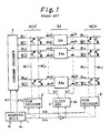
- Figure 1 illustrates a prior art DRAM device, which is a shared sense amplifier type device having, two memory cell arrays MCA and MCA′ are arranged on both sides of sense amplifiers SA1, SA2, ..., and SA m , and two pair of folded bit lines such as BL1 and BL 1′, and BL1′ and BL 1 are connected to one of the sense amplifiers such as SA1.
- Reference numeral 1 designates an address multiplexer for receiving address signals A l through A n from the address buffer (not shown) to generate multiple X-address signals AX l through AX n and Y-address signals AY l through AY n .
- Reference numerals 2 and 2′ designate row decoders for selecting one of the word lines WL1, WL2, ... (or WL1′, WL2′, ...) of the memory cell arrays MCA and MCA′ in accordance with the X-address signals AX l through AX n .
- Reference numeral 3 designates a column decoder for selecting one pair of the bit lines such BL1 and BL 1 (BL1′ and BL 1′) of the memory cell arrays MCA and MCA′ in accordance with the Y-address signals AY l through AY n .
- Reference numeral 4 designates a clock generator for generating a clock signal BT or BT′ in accordance with the X-address signal AX n and the clock signal ⁇ s from the RAS clock system (not shown).
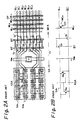
- transfer gates Q T and Q T ′ are provided on the bit lines BL1, BL 1, ..., BL1′, BL 1′, ... between the sense amplifiers SA1, SA2, ..., SA m and the memory cell arrays MCA and MCA′.
- one-transistor, one-capacitor type memory cells such as MC11 are provided mosaicly at intersections between the word lines and the bit lines.
- each of the sense amplifiers SA1, SA2, ... is formed by two cross-coupled N-channel MOS transistors Q ns and Q ns ′, which are enabled by a low potential of a clock signal NSA.
- each of the sense amplifiers also has two cross-coupled P-channel MOS transistors Q ps and Q ps ′, which are enabled by a high potential of a clock signal PSA, (not shown in Figs. 2A and 2B, but shown in Figs. 11A and 11B).
- the memory cell array MCA has a cell plate CP common to all memory cells.
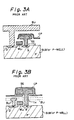
- This cell plate CP serves as a conductive shield plate for reducing the parasitic electrostatic capacity between the bit lines such as BL1 and BL 1, as showns in Figs. 3A and 3B, which illustrate one memory cell.
- a word line WL1 which serves as a gate electrode, is formed by depositing polycristalline silicon with a CVD method via the gate insulator (not shown) on the substrate SUB.
- a storage electrode SE is formed by depositing polycrystalline silicon by a CVD method via a through hole TH on the source region S, and a common cell plate CP is formed opposite to the storage SE, with the insulating layer (not shown) therebetween, thus forming a cell capacitor.
- a bit line such as BL1 is formed on the cell plate CP. Therefore, in this case, the cell plate CP cannot properly serve as a conductive shield layer for the bit lines, since the cell plate CP covers only a part of the lower surface of the bit lines.
- a common cell plate CP is formed thereon, so that the common cell plate CP completely covers the memory cell array MCA, particularly, the bit lines within the memory cell array MCA. Also, since the cell plate CP covers the both sides of the bit lines as well as the upper surface thereof, the shield effect of the cell plate CP against the bit lines is remarkably increased compared with that of the cell plate CP of Fig. 3A. This contributes to the reduction of the parasitic electrostatic capacity between the bit lines.
- the memory cell array MCA, the transfer gates Q T and Q T ′, and one part sense amplifiers SA1, SA2, ... enabled by the clock signal NSA are formed on a P-well, and therefore, a bias voltage V BB is applied thereto.
- the substrates SUB of Figs. 3A and 3B are formed by the P-well.
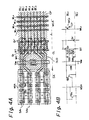
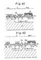
- a conductive shield plate SLD is added to the device of Figs. 2A and 2B.
- This conductive shield plate SLD covers the portion CL in which the transfer gates Q T and the bias voltage line for V BB are formed.
- the cell plate CP of Fig. 3B is used, as illustrated in Fig. 4C.
- the conductive shield plate SLD is integrated with the cell plate CP of the memory cell array MCA, i.e., the conductive shield plate SLD and the cell plate CP are made of the same metal layer such as polycrystalline, and therefore, the addition of the conductive shield plate SLD is carried out without increasing the number of manufacturing steps.
- a well bias voltage line V BB which is made of aluminium, is deposited via a well contact WC to the P-well region.
- the voltage of the well bias voltage line V BB is, for example, -1.5 V.
- two separate well bias voltage lines V BB1 and V BB2 having voltages 0 V and -1.5 V respectively, are connected to the P-well region for the transfer gates Q T and the P-well region for the memory cell array MCA.
- each bit line is about 1 ⁇ m, and the thickness thereof is about 0.2 ⁇ m. Also, the spacing between the bit lines is about 1.5 ⁇ m.
- the parasitic electrostatic capacity CBS between the conductive shield plate SLD including the cell plate CP and each bit line is increased to thus reduce the parasitic electrostatic capacity CBB between the bit lines.
- a potential at one bit line generated during a read operation has little affect on potentials at other adjacent bit lines.
- each bit line is able to withstand the affects of noise generated at bit lines adjacent thereto, and thus an erroneous write operation due to a read operation can be avoided.
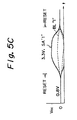
- Figs. 5A and 5B which illustrate a second embodiment of the present invention
- the conductive shield plate SLD is separate from the cell plate CP and is connected to a power supply source such as the ground. Nevertheless, the conductive shield plate SLD and the cell plate CP are made of the same material as used in the first embodiment of Figs. 4A through 4D.
- the separation of the conductive shield plate SLD and the cell plate CP is particularly effective when the amplitude of the restore voltage at the bit lines is different from the amplitude of the sense voltage of the sense amplifiers.
- a reset voltage for the bit lines is 0.8 V
- a restore voltage i.e., a rewritten voltage of "1”
- a reset voltage for the sense amplifiers is assumed to be 0.8 V.
- the drive of the sense amplifiers is carried out by using an external power supply voltage such as 3.3 V, and thus the sense voltage is amplified to 3.3 V.
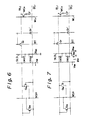
- a resistor R SD is inserted between the conductive shield plate SLD and the ground in Figs. 5A and 5B. If the resistor R SD is not included, as in the device of Figs. 5A and 5B, when the sense amplifier is operated so that a noise supplied to the conductive shield plate SLD is supplied directly to the power supply such as the ground, such a noise also is transferred in other circuits, via the power supply. To avoid this, the resistor R is provided to smooth the noise with a time constant ⁇ determined by CBS x R SD x n, where n is the number of bit lines. If this time constant is too large, however, a shield effect of the conductive shield plate SLD is reduced.
- the above-mentioned time constant ⁇ must be smaller than a value which corresponds, for example, to a half of a cycle time of a row address strobe (RAS) signal.
- resistor R SD can be introduced into the conductive shield plate SLD, if the conductive shield plate SLD is made of high resistance polycrystalline silicon.
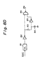
- Fig. 7 which is a fourth embodiment of the present invention, an N-channel MOS transistor Q SD is added to the device of Fig. 6, and the transistor Q SD is controlled by a clock signal ⁇ SD , which is turned OFF after the activation of the sense amplifiers before a completion of the operation of the sense amplifiers.
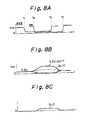
- the clock signal ⁇ SD is explained with reference to Figs. 8A through 8C.
- the clock signal ⁇ SD remains high and the transistor Q SD is turned ON, i.e., the conductive shield plate SLD is grounded to thereby exhibit a shielding effect.
- the state of the sense amplifiers is determined, the conductive shield plate SLD is no longer present, and the clock signal ⁇ SD falls to turn OFF the transistor Q SD .
- the conductive shield plate SLD becomes substantially in a floating state, due to the OFF state of the transistor Q SD , and therefore, when the mean voltage of the bit lines near the sense amplifiers is increased from 0.8 V to 1.65 V, the voltage of the conductive shield plate SLD follows this mean voltage, as shown in Figs. 8B and 8C.
- the sense voltages of the sense amplifiers are reset to 0.8 V as shown in Fig. 8B, and accordingly, the voltage of the conductive shield plate SLD falls as shown in Fig. 8C.
- the clock signal ⁇ SD returns to the initial stage.
- Fig. 8D designates a delay circuit, 82 an invester, 83 a resistor, 84 a capacitor, 85 an invester, and 86 a NAND circuit.
- the change of the voltage of the conductive shield plate SLD due to the change of the mean voltage of the bit lines near the sense amplifiers is not led to the power supply (the ground), and thus the power consumption is reduced.
- the resistor R SD can be omitted, i.e., the above-mentioned time constant ⁇ has a lower limit equal to a half of a RAS cycle, but has no upper limit, and therefore, the value of the resistor R SD can be made infinite, i.e., the resistor R SD can be omitted.
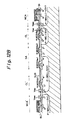
- the conductive shield plate SLD also covers the sense amplifier portion SA, to further exhibit a shield effect for noise generated between the bit lines.
- active areas for the source and drain regions of the cell transistors are indicated by AR.
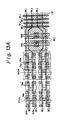
- FIGs. 11A and 11B which are modifications of Figs. 4A and 4B, P-channel MOS transistors Q ps and Q ps ′ are added to each of the sense amplifiers SA1, SA2, ....
- Fig. 12A which is a modification of Fig. 5A, P-channel MOS transistors Q ps and Q ps ′ are added to each of the sense amplifiers SA1, SA2, ....
- the P-channel transistors Q ps and Q ps ′ are enabled by a low potential of a clock signal PSA.
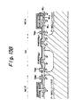
- Figure 12B is a cross-section view of Fig. 12A, the P-channel transistor of the sense amplifier portion SA, the transfer gate portion CL′, and the memory cell array MCA′ are also illustrated in addition to Fig. 4D.
- FIGs. 13A and 13B which are modifications of Figs. 12A and 12B, an open bit line type device is illustrated. In this device, the transfer gates Q T and Q T ′ are unnecessary. Note, the present invention obviously can be applied to a simple folded bit line type DRAMs.
- the parasitic electrostatic capacity between the bit lines can be reduced by the conductive shield plate, an erroneous operation due to noise between the bit lines can be avoided. Also, since the provision of the conductive shield plate does not increase the occupied area of the device, the integration thereof is not reduced.
Landscapes
- Engineering & Computer Science (AREA)
- Microelectronics & Electronic Packaging (AREA)
- Computer Hardware Design (AREA)
- Semiconductor Memories (AREA)
- Dram (AREA)
Applications Claiming Priority (2)
| Application Number | Priority Date | Filing Date | Title |
|---|---|---|---|
| JP2127524A JP2746730B2 (ja) | 1990-05-17 | 1990-05-17 | 半導体記憶装置 |
| JP127524/90 | 1990-05-17 |
Publications (3)
| Publication Number | Publication Date |
|---|---|
| EP0457591A2 true EP0457591A2 (de) | 1991-11-21 |
| EP0457591A3 EP0457591A3 (en) | 1992-10-21 |
| EP0457591B1 EP0457591B1 (de) | 1996-04-03 |
Family
ID=14962150
Family Applications (1)
| Application Number | Title | Priority Date | Filing Date |
|---|---|---|---|
| EP91304409A Expired - Lifetime EP0457591B1 (de) | 1990-05-17 | 1991-05-16 | Halbleiterspeicheranordnung mit reduzierten parasitären Kapazitäten zwischen Bitleitungen |
Country Status (5)
| Country | Link |
|---|---|
| US (1) | US5808334A (de) |
| EP (1) | EP0457591B1 (de) |
| JP (1) | JP2746730B2 (de) |
| KR (1) | KR950008671B1 (de) |
| DE (1) | DE69118436T2 (de) |
Cited By (1)
| Publication number | Priority date | Publication date | Assignee | Title |
|---|---|---|---|---|
| WO2003030176A3 (en) * | 2001-09-28 | 2003-12-31 | Infineon Technologies Ag | Memory array employing integral isolation transistors |
Families Citing this family (10)
| Publication number | Priority date | Publication date | Assignee | Title |
|---|---|---|---|---|
| US6947324B1 (en) | 2000-06-28 | 2005-09-20 | Marvell International Ltd. | Logic process DRAM |
| US6570781B1 (en) * | 2000-06-28 | 2003-05-27 | Marvell International Ltd. | Logic process DRAM |
| US7184290B1 (en) | 2000-06-28 | 2007-02-27 | Marvell International Ltd. | Logic process DRAM |
| JP2004040042A (ja) * | 2002-07-08 | 2004-02-05 | Fujitsu Ltd | 半導体記憶装置 |
| JP4015968B2 (ja) * | 2003-06-09 | 2007-11-28 | 株式会社東芝 | 強誘電体メモリ |
| US6822891B1 (en) * | 2003-06-16 | 2004-11-23 | Kabushiki Kaisha Toshiba | Ferroelectric memory device |
| JP2005322380A (ja) * | 2004-04-09 | 2005-11-17 | Toshiba Corp | 半導体記憶装置 |
| JP4781783B2 (ja) | 2005-10-31 | 2011-09-28 | エルピーダメモリ株式会社 | 半導体記憶装置 |
| TWI683418B (zh) | 2018-06-26 | 2020-01-21 | 華邦電子股份有限公司 | 動態隨機存取記憶體及其製造、寫入與讀取方法 |
| CN110718549A (zh) * | 2018-07-12 | 2020-01-21 | 华邦电子股份有限公司 | 动态随机存取存储器及其制造、写入与读取方法 |
Family Cites Families (7)
| Publication number | Priority date | Publication date | Assignee | Title |
|---|---|---|---|---|
| US3811076A (en) * | 1973-01-02 | 1974-05-14 | Ibm | Field effect transistor integrated circuit and memory |
| JPS5862893A (ja) * | 1981-10-09 | 1983-04-14 | Mitsubishi Electric Corp | Mosダイナミツクメモリ |
| JPH0664907B2 (ja) * | 1985-06-26 | 1994-08-22 | 株式会社日立製作所 | ダイナミツク型ram |
| US4791616A (en) * | 1985-07-10 | 1988-12-13 | Fujitsu Limited | Semiconductor memory device |
| KR910009805B1 (ko) * | 1987-11-25 | 1991-11-30 | 후지쓰 가부시끼가이샤 | 다이나믹 랜덤 액세스 메모리 장치와 그의 제조방법 |
| JPH021928A (ja) * | 1988-06-10 | 1990-01-08 | Toshiba Corp | 半導体集積回路 |
| US5057887A (en) * | 1989-05-14 | 1991-10-15 | Texas Instruments Incorporated | High density dynamic ram cell |
-
1990
- 1990-05-17 JP JP2127524A patent/JP2746730B2/ja not_active Expired - Fee Related
-
1991
- 1991-05-16 EP EP91304409A patent/EP0457591B1/de not_active Expired - Lifetime
- 1991-05-16 DE DE69118436T patent/DE69118436T2/de not_active Expired - Fee Related
- 1991-05-17 KR KR1019910008083A patent/KR950008671B1/ko not_active Expired - Fee Related
-
1994
- 1994-11-14 US US08/340,318 patent/US5808334A/en not_active Expired - Fee Related
Cited By (1)
| Publication number | Priority date | Publication date | Assignee | Title |
|---|---|---|---|---|
| WO2003030176A3 (en) * | 2001-09-28 | 2003-12-31 | Infineon Technologies Ag | Memory array employing integral isolation transistors |
Also Published As
| Publication number | Publication date |
|---|---|
| JP2746730B2 (ja) | 1998-05-06 |
| EP0457591A3 (en) | 1992-10-21 |
| US5808334A (en) | 1998-09-15 |
| DE69118436D1 (de) | 1996-05-09 |
| DE69118436T2 (de) | 1996-08-14 |
| KR950008671B1 (ko) | 1995-08-04 |
| JPH0422169A (ja) | 1992-01-27 |
| EP0457591B1 (de) | 1996-04-03 |
Similar Documents
| Publication | Publication Date | Title |
|---|---|---|
| KR100397684B1 (ko) | 메모리장치,집적회로구조물및다이나믹램설계를최소화하기위한방법 | |
| US4477736A (en) | Semiconductor integrated circuit device including means for reducing the amount of potential variation on a reference voltage line | |
| US6584031B2 (en) | Semiconductor integrated circuit device | |
| KR100218622B1 (ko) | 면적효율이 우수한 용량소자를 갖는 반도체장치 | |
| US5866928A (en) | Single digit line with cell contact interconnect | |
| JP2929430B2 (ja) | キャパシタがないdramおよびその製造方法 | |
| EP0046011B1 (de) | Halbleiterspeicheranordnung | |
| JPS5826830B2 (ja) | 集積回路メモリ・アレイ | |
| US6532167B2 (en) | Voltage generator for semiconductor device | |
| EP0457591B1 (de) | Halbleiterspeicheranordnung mit reduzierten parasitären Kapazitäten zwischen Bitleitungen | |
| EP1181694B1 (de) | Plattenleitungslesen | |
| US5850090A (en) | Dynamic semiconductor memory device on SOI substrate | |
| KR930000759B1 (ko) | 다이나믹 메모리 | |
| KR20000071473A (ko) | 반도체 메모리 장치 | |
| US4916666A (en) | Dynamic random access memory device and operating method therefor | |
| US5666306A (en) | Multiplication of storage capacitance in memory cells by using the Miller effect | |
| JPH09232531A (ja) | 半導体記憶装置 | |
| US6002636A (en) | Semiconductor memory drive capable of canceling power supply noise | |
| US6115309A (en) | Sense amplifier having increased drive current capability | |
| US4771322A (en) | Semiconductor memory device with low-noise structure | |
| US6172897B1 (en) | Semiconductor memory and write and read methods of the same | |
| US5761112A (en) | Charge storage for sensing operations in a DRAM | |
| JP2940485B2 (ja) | 半導体記憶装置 | |
| EP0128273B1 (de) | Integrierter Halbleiterspeicher | |
| US5995410A (en) | Multiplication of storage capacitance in memory cells by using the Miller effect |
Legal Events
| Date | Code | Title | Description |
|---|---|---|---|
| PUAI | Public reference made under article 153(3) epc to a published international application that has entered the european phase |
Free format text: ORIGINAL CODE: 0009012 |
|
| AK | Designated contracting states |
Kind code of ref document: A2 Designated state(s): DE FR GB IT |
|
| PUAL | Search report despatched |
Free format text: ORIGINAL CODE: 0009013 |
|
| AK | Designated contracting states |
Kind code of ref document: A3 Designated state(s): DE FR GB IT |
|
| 17P | Request for examination filed |
Effective date: 19921102 |
|
| 17Q | First examination report despatched |
Effective date: 19950405 |
|
| ITF | It: translation for a ep patent filed | ||
| GRAH | Despatch of communication of intention to grant a patent |
Free format text: ORIGINAL CODE: EPIDOS IGRA |
|
| GRAA | (expected) grant |
Free format text: ORIGINAL CODE: 0009210 |
|
| AK | Designated contracting states |
Kind code of ref document: B1 Designated state(s): DE FR GB IT |
|
| PG25 | Lapsed in a contracting state [announced via postgrant information from national office to epo] |
Ref country code: FR Effective date: 19960403 |
|
| REF | Corresponds to: |
Ref document number: 69118436 Country of ref document: DE Date of ref document: 19960509 |
|
| EN | Fr: translation not filed | ||
| PLBE | No opposition filed within time limit |
Free format text: ORIGINAL CODE: 0009261 |
|
| STAA | Information on the status of an ep patent application or granted ep patent |
Free format text: STATUS: NO OPPOSITION FILED WITHIN TIME LIMIT |
|
| 26N | No opposition filed | ||
| REG | Reference to a national code |
Ref country code: GB Ref legal event code: IF02 |
|
| PGFP | Annual fee paid to national office [announced via postgrant information from national office to epo] |
Ref country code: DE Payment date: 20070510 Year of fee payment: 17 |
|
| PGFP | Annual fee paid to national office [announced via postgrant information from national office to epo] |
Ref country code: GB Payment date: 20070516 Year of fee payment: 17 |
|
| PGFP | Annual fee paid to national office [announced via postgrant information from national office to epo] |
Ref country code: IT Payment date: 20070528 Year of fee payment: 17 |
|
| GBPC | Gb: european patent ceased through non-payment of renewal fee |
Effective date: 20080516 |
|
| PG25 | Lapsed in a contracting state [announced via postgrant information from national office to epo] |
Ref country code: DE Free format text: LAPSE BECAUSE OF NON-PAYMENT OF DUE FEES Effective date: 20081202 |
|
| PG25 | Lapsed in a contracting state [announced via postgrant information from national office to epo] |
Ref country code: GB Free format text: LAPSE BECAUSE OF NON-PAYMENT OF DUE FEES Effective date: 20080516 |
|
| PG25 | Lapsed in a contracting state [announced via postgrant information from national office to epo] |
Ref country code: IT Free format text: LAPSE BECAUSE OF NON-PAYMENT OF DUE FEES Effective date: 20080516 |