EP0454859A1 - Integrierte halbleiterschaltung - Google Patents
Integrierte halbleiterschaltung Download PDFInfo
- Publication number
- EP0454859A1 EP0454859A1 EP90916371A EP90916371A EP0454859A1 EP 0454859 A1 EP0454859 A1 EP 0454859A1 EP 90916371 A EP90916371 A EP 90916371A EP 90916371 A EP90916371 A EP 90916371A EP 0454859 A1 EP0454859 A1 EP 0454859A1
- Authority
- EP
- European Patent Office
- Prior art keywords
- voltage
- power source
- semiconductor
- external power
- circuit
- Prior art date
- Legal status (The legal status is an assumption and is not a legal conclusion. Google has not performed a legal analysis and makes no representation as to the accuracy of the status listed.)
- Granted
Links
- 239000004065 semiconductor Substances 0.000 claims abstract description 103
- 238000010586 diagram Methods 0.000 description 21
- 239000002784 hot electron Substances 0.000 description 5
- 230000005684 electric field Effects 0.000 description 3
- 238000000034 method Methods 0.000 description 3
- 230000000694 effects Effects 0.000 description 2
- 230000007257 malfunction Effects 0.000 description 2
- 235000001537 Ribes X gardonianum Nutrition 0.000 description 1
- 235000001535 Ribes X utile Nutrition 0.000 description 1
- 235000016919 Ribes petraeum Nutrition 0.000 description 1
- 244000281247 Ribes rubrum Species 0.000 description 1
- 235000002355 Ribes spicatum Nutrition 0.000 description 1
- 230000004913 activation Effects 0.000 description 1
- 230000002411 adverse Effects 0.000 description 1
- 230000032683 aging Effects 0.000 description 1
- 230000006378 damage Effects 0.000 description 1
- 230000010354 integration Effects 0.000 description 1
- 230000004044 response Effects 0.000 description 1
Images


Classifications
-
- H—ELECTRICITY
- H01—ELECTRIC ELEMENTS
- H01L—SEMICONDUCTOR DEVICES NOT COVERED BY CLASS H10
- H01L27/00—Devices consisting of a plurality of semiconductor or other solid-state components formed in or on a common substrate
- H01L27/02—Devices consisting of a plurality of semiconductor or other solid-state components formed in or on a common substrate including semiconductor components specially adapted for rectifying, oscillating, amplifying or switching and having potential barriers; including integrated passive circuit elements having potential barriers
- H01L27/0203—Particular design considerations for integrated circuits
- H01L27/0214—Particular design considerations for integrated circuits for internal polarisation, e.g. I2L
- H01L27/0218—Particular design considerations for integrated circuits for internal polarisation, e.g. I2L of field effect structures
Definitions
- the present invention relates to a semiconductor integrated circuit, and more particularly, relates to a semiconductor integrated circuit for dropping an external power source voltage to thereby obtain an internal power source voltage.
- the miniaturizing a semiconductor elements is continued because the integration level of semiconductor integrated circuits can be thus enhanced. Nevertheless, this miniaturizing of the semiconductor elements leads to such disadvantages as a lowering of the pressure resistance thereof and the possibility that the element will be adversely influenced by hot electrons.
- the measure of lowering the power source voltage to be supplied to the semiconductor element, to minimize the electric field strength of the respective portions of the element is effective.
- the destruction by aging of an oxidated film can be prevented by lowering the electric field strength of the oxidated film.
- the generation of hot electrons can be suppressed, to thereby reduce the amount of hot electrons injected into the oxidated film, i.e., the hot electron instability (concretely, the variation of threshold value V th and a poor conductance) can be prevented.
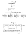
- Fig. 1 and Fig. 2 show the structure of a conventional semiconductor integrated circuit for dropping the external power source voltage inside the semiconductor integrated circuit to produce a low voltage internal power source.
- VccPAD is a power source terminal installed at a semiconductor chip, to which the external power source is to be applied
- "A" is a voltage drop circuit
- C11 through C1n represent a plurality ("n" units) of semiconductor circuits.
- the power source terminal VccPAD is installed, usually as one body, on the semiconductor chip 2, and the semiconductor circuits C11 through C1n are two-dimensionally arranged in the plane of the semiconductor chip 2.
- the voltage drop circuit "A” forms an internal power source voltage Vint, which drops the external power source voltage applied to the power source terminal VccPAD, to a given voltage.
- This external voltage is a common power source voltage which is also applied to the other semiconductor integrated circuits and is, for example, +5 V. The voltage is dropped to a given level by utilizing, for example, the channel resistance of a MOS transistor.
- the given voltage referred to herein means the voltage necessary for the actuation of a miniaturized semiconductor element (for example, a MOS transistor) forming a structure of a plurality of internal semiconductor circuits C11 through C1n, and moreover, which effectively avoids a pressure resistance and hot electrons.
- a miniaturized semiconductor element for example, a MOS transistor
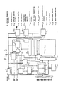
- Fig. 3 shows an example of semiconductor circuits C11 through C1n given in Fig. 1, where the semiconductor integrated circuit is a dynamic RAM.
- C11 is a mode control circuit
- C12 a refresh address counter
- C13 an address buffer
- C14 a pre-decoder
- C15 a basic bias generating circuit
- C16 a sense amplifier driver
- C17 a first clock generating circuit
- C18 a gate circuit
- C20 a write clock generating circuit
- C23 a date input buffer and C24 a data output buffer and the internal power source voltage, which has been dropped by the voltage drop circuit "A"
- Fig. 4A is a circuit diagram showing the structure example of the address buffer of Fig. 3
- Fig. 4B is a circuit diagram showing the structure example of the pre-decoder of Fig. 3.
- a technique is employed such as installing a circuit to detect the voltage drop of the internal power source voltage Vint, and supplying a comparatively large current when the voltage drop has been detected, thus suppress the fluctuations of internal power source voltage.
- a delay in the response, to a certain degree, was unavoidable until the current was supplied after the actual voltage drop, and as a result, the conventional circuit could not properly effectively suppress the instantaneous voltage drop of internal power source voltage Vint.
- an object of this invention is to provide a semiconductor integrated circuit capable of effectively suppressing voltage fluctuations in an internal power source voltage, and which will prevent a malfunction of the semiconductor circuits even if a semiconductor circuit consuming a large current is actuated.
- an external power source terminal is connected to the inside of the semiconductor chip, a plurality of voltage dropping means are installed for altering the external power source voltage into a desired internal power source voltage, and at least 1 block of a plurality of semiconductor circuit blocks arranged inside the semiconductor chip are connected to each of said voltage dropping means.
- an exclusive-use internal power source voltage is formed for each of several semiconductor circuits, and the influence of other internal power source voltages can be avoided if a fluctuation of a single internal power source voltage should occur.
- Fig. 5 is a block circuit diagram showing the structure of semiconductor integrated circuit related to the present invention.
- VccPAD indicates a power source terminal for an external power source
- A1 through An are voltage dropping circuits
- C11 through C1n are semiconductor circuit blocks, respectively.
- the voltage dropping circuits A1 through An are installed for each of a plurality of semiconductor internal circuits (semiconductor circuit blocks) C11 through C1n, for dropping the external power source voltage Vcc applied to the power source terminal VccPAD to a given voltage by utilizing, for example, the channel resistance of a MOS transistor, to thus form internal power source voltages from Vint1 through Vintn, respectively.
- a plurality of semiconductor circuit blocks C11 through C1n are respective functional blocks formed on the semiconductor integrated circuit.
- DRAM dynamic RAM
- such functional blocks as a clock generator and memory cell array (including the sense amplifier) are semiconductor circuit blocks.
- Fig. 6 shows concrete circuit examples of semiconductor circuits C11 through C1n when the semiconductor integrated circuits are DRAMs, and the same symbols are given as given to identical members of the conventional semiconductor integrated circuit shown in Fig. 3.
- Fig. 6 shows concrete circuit examples of semiconductor circuits C11 through C1n when the semiconductor integrated circuits are DRAMs, and the same symbols are given as given to identical members of the conventional semiconductor integrated circuit shown in Fig. 3.
- Fig. 6 shows concrete circuit examples of semiconductor circuits C11 through C1n when the semiconductor integrated circuits are DRAMs, and the same symbols are given as given to identical members of the conventional semiconductor integrated circuit shown in Fig. 3.
- Fig. 6 shows concrete circuit examples of semiconductor circuits C11 through C1n when the semiconductor integrated circuits are DRAMs, and the same symbols are
- C11 is a mode control circuit, C12 a refresh address counter C13 an addresss buffer, C14 a pre-decoder, C15 a basic bias generating circuit, C16 a sense amplifier driver, C17 a 1st clock generating circuit, C18 a gate circuit, C19 a 2nd clock generating circuit, C20 a write clock generating circuit, C21 a column decoder, C22 a low decoder, C23 a data input buffer and C24 a data output buffer, respectively, and the internal power source voltage which has been dropped by the voltage dropping circuits A1 through A5 is to be supplied to each of these semiconductor circuits C11 through C24.
- the address buffer C13 and the pre-decoder C14 have the same structures as those shown in Fig. 4A and Fig. 4B.
- the mode control circuit C11 , refresh address counter C12 , address buffer C13 , pre-decoder c14 , basic bias generating circuit C15 and low decoder C22 corresponds to the semiconductor circuit C11 of Fig. 5, and are activated by the internal power source voltage Vint1 from the voltage dropping circuit A1.
- the sense amplifier driver C16 corresponds to the semiconductor circuit C12 of Fig. 5 and is activated by the internal power source voltage Vint2 from the voltage dropping circuit A2.
- the 1st clock generating circuit C17 , gate circuit C18 , 2nd clock generating circuit C19 and column decoder C21 correspond to the semiconductor circuit C13 of Fig. 5 and are activated by the internal power source voltage Vint3 from the voltage dropping circuit A3.
- the data input buffer C23 and the data output buffer C24 correspond to the semiconductor circuit C14 and are activated by the internal power source voltage Vint4 from the voltage dropping circuit A4, and the write clock generating circuit C20 corresponds to the semiconductor circuit C15 and is activated by the internal power source voltage Vint5 from the voltage dropping circuit A5.
- the operating current of a memory cell array inclusive of the sense amplifier is very high, and therefore, during the actuation of the memory cell array, the current flowing through the voltage dropping circuit A is increased and an instantaneous voltage drop of the internal power source voltage Vint1 occurs. Because, however, in this embodiment this internal power source voltage Vint1 is independent of the internal power source voltages Vint2 through Vint5 of other semiconductor circuits C12 through C15, the voltage drops of other internal power source voltages Vint2 through Vint5 can be suppressed even if the power drop occurs in a single internal power source voltage Vint1.
- Fig. 7 through Fig. 9 are diagrams showing the structures of other embodiments of semiconductor integrated circuits related to the present invention.
- Fig. 7 indicates an example of the structure, using respective MOS transistors, of the voltage dropping means A11 through A1n installed at each of a plurality of semiconductor circuit blocks C11 through C1n.
- the source of each MOS transistor is connected to the external power source terminal VccPAD via a common line L, and further, the gate of each MOS transistor is also connected to the external power source terminal VccPAD via the common line L.
- the resistances R1 through Rn in the common line L represent the wiring resistance between the power source terminal VccPAD and the respective MOS transistors.
- each of internal power source voltages Vint2 through Vintn is lowered by the channel resistance of the MOS transistor to the power source voltage Vcc.
- Fig. 8 illustrates another example of the structure of, using MOS transistors, the voltage dropping means A11 through A1n installed at each of a plurality of semiconductor circuit blocks C11 through C1n, and the same symbols are given to the same component parts as those of Fig. 7.
- the source of each MOS transistor is connected to the external power source terminal VccPAD via the 1st common line L1
- the gate of each MOS transistor is connected to the external power source terminal VccPAD via the 2nd common line L2.
- the resistances R1 through Rn in the 1st common line L1 represent the wiring resistance between the power source terminal VccPAD and the respective MOS transistors.
- the potentials VN1 , VN2 , ... VN n of respective nodes N1 ... Nn in the 1st common line L1 can be expressed by each of the following formulae.
- V R1 , V R2 , ... V Rn are given as the multiplied values of the current I mA and the resistance R1 (or R2 ... Rn), and therefore, if a large current (I mA) flows into a single semiconductor circuit (C1n), the other semi-conductor circuits C11, C12 ... are subjected to the influence of the voltage drop portions V R1 , V R2 ... etc.
- C1n can be made the constant potentials which have been lowered by the threshold value V th portion of MOS transistor from the external power source potential Vcc, even if a voltage drop occurs at the nodes N1 ... Nn, and (iii) the influence of a voltage drop by the wiring resistances R1 ... Rn in the 1st common line L1 can be effectively avoided.
- the internal power source voltage Vint2 for example, of the semiconductor circuit C12 given at the voltage lower by the threshold value V th portion of MOS transistor from the external power source potential Vcc as shown in Fig. 11 is not subjected to the influence of the aforementioned potential difference ⁇ VN2, or even if subjected such an influence is slight, and can maintain an almost constant potential (Vcc - V th ) because the gate potential of MOS transistor is maintained approximately at the external power source potential Vcc by the 2nd common line L2, which is an exclusive-use wiring, even if the potential VN2 of node N2 is lowered by the potential difference ⁇ VN2 at the time t1.
- the dotted line in Fig. 11 is the voltage waveform of Fig. 7 connected to the same node with the gate source of MOS transistor used in common, and the internal power source voltage Vint2 is greatly fluctuated by the voltage fluctuation of node.
- Fig. 9 shows a transformed pattern of the embodiment given in Fig. 8; identical symbols are given to the same structural portions as those of Fig. 8.
- the gate of each MOS transistor in the structure of the voltage dropping circuits A11 through A1n is connected to the 2nd common line L2 via the voltage drop controlling circuits G1, G2 ... Gn.
- G2 is activated by the individual selection signals S1 ...
- the 2nd common line L2 is connected to the gate of MOS transistor A12 via the voltage drop controlling circuit G2 under activation, and thus the gate potential of the MOS transistor can be maintained at approximately the power source voltage Vcc, and thus an effect similar to that of the embodiment shown in Fig. 8 is obtained.
- the power source supply to the respective semiconductor circuit blocks C11 through C1n can be switched ON and OFF by the individual selection signals S1 through Sn, it is preferably applied to the semiconductor integrated circuit in which an attempt is made to obtain a lower power consumption by dividing, for example, the memory cell array into a plurality of blocks and switching off the power source supply in non-operating blocks.
- Fig. 10 shows the transformed embodiment of a concrete example of the semiconductor circuit blocks C11 through C1n in accordance with the present invention, where the semiconductor integrated circuit shown in Fig. 6 is a DRAM, and is an example of the case wherein the voltage of the external power source does not fail, because the characteristics of the device are to be applied, as is, to the data input buffer C23 and the data output buffer C24. Because the voltage dropping circuits are installed respectively at each of semiconductor circuits in the semiconductor integrated circuit of this invention, a transformed embodiment considering the characteristics of device is thus available. Further, although the internal power source voltage of the sense amplifier driver C16 is formed by the voltage dropping circuit A2 in the circuit in Fig. 10, this voltage dropping circuit A2 need not to be installed at the sense amplifier driver which per se has an external power source voltage dropping action.
- Fig. 12 shows a circuit diagram of another embodiment of the voltage dropping circuit, as used in the embodiments explained above, and is an example of a voltage dropping circuit using a plurality of MOS transistors.
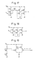
- Fig. 13 and Fig. 14 are circuit diagrams showing the concrete circuit structural examples of the voltage drop controlling circuits of Fig. 9, and are examples of cases where the voltage drop potential is the external power source voltage Vcc and the threshold value voltage is V th . Therefore, because the threshold value voltage is about 1 V when the external power source voltage Vcc is 5 V, the internal power source voltage in the semiconductor integrated circuit using the circuit in this embodiment is about 4 V.
- Fig. 15 through Fig. 18 are circuit diagrams showing other Concrete circuit structural examples of the voltage drop controlling circuits of Fig. 9, and are examples of cases in which the voltage drop potential is the external power source voltage Vcc and the threshold value voltage is 2 V th . Therefore, because the threshold value voltage is about 1 V when the external power source voltage Vcc is 5 V, the internal power source voltage in the semiconductor integrated circuit using the circuit of this embodiment is about 3 V.
- Fig. 19 is a circuit diagram showing another concrete circuit structural example of the voltage drop controlling circuit of Fig. 9, and shows a circuit structure whereby the voltage drop potential can be optionally set up.
Landscapes
- Engineering & Computer Science (AREA)
- Power Engineering (AREA)
- Physics & Mathematics (AREA)
- Condensed Matter Physics & Semiconductors (AREA)
- General Physics & Mathematics (AREA)
- Computer Hardware Design (AREA)
- Microelectronics & Electronic Packaging (AREA)
- Dram (AREA)
- Semiconductor Integrated Circuits (AREA)
- Semiconductor Memories (AREA)
Applications Claiming Priority (3)
| Application Number | Priority Date | Filing Date | Title |
|---|---|---|---|
| JP289118/89 | 1989-11-07 | ||
| JP1289118A JP3009109B2 (ja) | 1989-11-07 | 1989-11-07 | 半導体集積回路 |
| PCT/JP1990/001444 WO1991006980A1 (en) | 1989-11-07 | 1990-11-07 | Semiconducteur integrated circuit |
Publications (3)
| Publication Number | Publication Date |
|---|---|
| EP0454859A1 true EP0454859A1 (de) | 1991-11-06 |
| EP0454859A4 EP0454859A4 (en) | 1993-01-20 |
| EP0454859B1 EP0454859B1 (de) | 1998-01-14 |
Family
ID=17739011
Family Applications (1)
| Application Number | Title | Priority Date | Filing Date |
|---|---|---|---|
| EP90916371A Expired - Lifetime EP0454859B1 (de) | 1989-11-07 | 1990-11-07 | Integrierte halbleiterschaltung |
Country Status (4)
| Country | Link |
|---|---|
| EP (1) | EP0454859B1 (de) |
| JP (1) | JP3009109B2 (de) |
| DE (1) | DE69031944T2 (de) |
| WO (1) | WO1991006980A1 (de) |
Families Citing this family (6)
| Publication number | Priority date | Publication date | Assignee | Title |
|---|---|---|---|---|
| KR0126243B1 (ko) * | 1992-06-29 | 1997-12-26 | 세끼자와 다다시 | 자기재생기능을 갖는 반도체 메모리장치 |
| JP2006203248A (ja) * | 1994-08-04 | 2006-08-03 | Renesas Technology Corp | 半導体装置 |
| JP4841658B2 (ja) * | 1995-10-06 | 2011-12-21 | ルネサスエレクトロニクス株式会社 | 半導体記憶装置 |
| JP2000164808A (ja) * | 1998-11-26 | 2000-06-16 | Nec Corp | 半導体装置 |
| JP4498500B2 (ja) * | 1999-10-06 | 2010-07-07 | 株式会社ルネサステクノロジ | 半導体装置 |
| JP3803050B2 (ja) | 2001-10-29 | 2006-08-02 | 株式会社ルネサステクノロジ | 半導体記憶装置、ダイナミックランダムアクセスメモリおよび半導体装置 |
Citations (1)
| Publication number | Priority date | Publication date | Assignee | Title |
|---|---|---|---|---|
| JPS62189695A (ja) * | 1986-02-17 | 1987-08-19 | Hitachi Ltd | 半導体装置 |
Family Cites Families (8)
| Publication number | Priority date | Publication date | Assignee | Title |
|---|---|---|---|---|
| JPS5423340A (en) * | 1977-07-22 | 1979-02-21 | Hitachi Ltd | Mis semiconductor integrated circuit |
| JPS55156354A (en) * | 1979-05-24 | 1980-12-05 | Nippon Telegr & Teleph Corp <Ntt> | Feeding method for large scale semiconductor ic |
| FR2494519A1 (fr) * | 1980-11-14 | 1982-05-21 | Efcis | Generateur de courant integre en technologie cmos |
| JPS5943421A (ja) * | 1982-09-06 | 1984-03-10 | Hitachi Ltd | 半導体集積回路 |
| JPS59112640A (ja) * | 1982-12-18 | 1984-06-29 | Toshiba Corp | 半導体集積回路 |
| JPS59110209A (ja) * | 1982-12-15 | 1984-06-26 | Mitsubishi Electric Corp | 相補形mos半導体集積回路 |
| JPS6273755A (ja) * | 1985-09-27 | 1987-04-04 | Toshiba Corp | 電源電圧降下回路 |
| JPH0648782B2 (ja) * | 1986-05-08 | 1994-06-22 | 日本電気株式会社 | 定電流源 |
-
1989
- 1989-11-07 JP JP1289118A patent/JP3009109B2/ja not_active Expired - Lifetime
-
1990
- 1990-11-07 DE DE69031944T patent/DE69031944T2/de not_active Expired - Fee Related
- 1990-11-07 WO PCT/JP1990/001444 patent/WO1991006980A1/ja active IP Right Grant
- 1990-11-07 EP EP90916371A patent/EP0454859B1/de not_active Expired - Lifetime
Patent Citations (1)
| Publication number | Priority date | Publication date | Assignee | Title |
|---|---|---|---|---|
| JPS62189695A (ja) * | 1986-02-17 | 1987-08-19 | Hitachi Ltd | 半導体装置 |
Non-Patent Citations (3)
| Title |
|---|
| IEEE JOURNAL OF SOLID-STATE CIRCUITS. vol. 22, no. 3, June 1987, NEW YORK US pages 437 - 441 T. FURUYAMA ET AL. 'A New On-chip Voltage Converter for Submicrometer High-Density DRAM's' * |
| PATENT ABSTRACTS OF JAPAN vol. 012, no. 043 (P-664)9 February 1988 & JP-A-62 189 695 ( HITACHI LTD. ) 19 August 1987 * |
| See also references of WO9106980A1 * |
Also Published As
| Publication number | Publication date |
|---|---|
| EP0454859A4 (en) | 1993-01-20 |
| JP3009109B2 (ja) | 2000-02-14 |
| DE69031944T2 (de) | 1998-05-28 |
| EP0454859B1 (de) | 1998-01-14 |
| WO1991006980A1 (en) | 1991-05-16 |
| JPH03149867A (ja) | 1991-06-26 |
| DE69031944D1 (de) | 1998-02-19 |
Similar Documents
| Publication | Publication Date | Title |
|---|---|---|
| US6985027B2 (en) | Voltage step down circuit with reduced leakage current | |
| KR960011936B1 (ko) | 게이트 어레이 장치, 입력 회로, 출력 회로 및 전압 강하 회로 | |
| KR960012001A (ko) | 파워 서플라이 선의 개선된 계층구조를 가지고 있는 반도체 기억장치 | |
| US6005434A (en) | Substrate potential generation circuit that can suppress variation of output voltage with respect to change in external power supply voltage and environment temperature | |
| JPH03505940A (ja) | 低電力電圧クランプ回路 | |
| JPH1173769A (ja) | 半導体装置 | |
| KR0170514B1 (ko) | 승압 전원을 갖는 반도체 메모리 장치 | |
| US4542485A (en) | Semiconductor integrated circuit | |
| KR960009158A (ko) | 기준전압 발생회로 | |
| US5966043A (en) | Power supply switching circuit | |
| EP0454859A1 (de) | Integrierte halbleiterschaltung | |
| US5786719A (en) | Mode setting circuit and mode setting apparatus used to select a particular semiconductor function | |
| JP3810220B2 (ja) | 内部電源供給発生器を有する集積回路半導体メモリ装置 | |
| US6777707B2 (en) | Semiconductor integrated circuit with voltage down converter adaptable for burn-in testing | |
| JPH07220484A (ja) | 電圧変換装置 | |
| US5315167A (en) | Voltage burn-in scheme for BICMOS circuits | |
| US5309040A (en) | Voltage reducing circuit | |
| US4904885A (en) | Substrate bias circuit having substrate bias voltage clamp and operating method therefor | |
| US5262989A (en) | Circuit for sensing back-bias level in a semiconductor memory device | |
| JP3262103B2 (ja) | 内部電源回路を有する半導体装置 | |
| US5691944A (en) | Non-volatile semiconductor memory device | |
| KR0144410B1 (ko) | 반도체 메모리 장치의 리스토어 회로 및 그 구조 | |
| JP3087677B2 (ja) | 半導体装置 | |
| US5467054A (en) | Output circuit for multibit-outputting memory circuit | |
| KR100190049B1 (ko) | 어레이회로 제어용 내부전압을 이용한 승압전원발생장치 |
Legal Events
| Date | Code | Title | Description |
|---|---|---|---|
| PUAI | Public reference made under article 153(3) epc to a published international application that has entered the european phase |
Free format text: ORIGINAL CODE: 0009012 |
|
| 17P | Request for examination filed |
Effective date: 19910726 |
|
| AK | Designated contracting states |
Kind code of ref document: A1 Designated state(s): DE FR GB |
|
| A4 | Supplementary search report drawn up and despatched |
Effective date: 19921127 |
|
| AK | Designated contracting states |
Kind code of ref document: A4 Designated state(s): DE FR GB |
|
| 17Q | First examination report despatched |
Effective date: 19950222 |
|
| GRAG | Despatch of communication of intention to grant |
Free format text: ORIGINAL CODE: EPIDOS AGRA |
|
| GRAG | Despatch of communication of intention to grant |
Free format text: ORIGINAL CODE: EPIDOS AGRA |
|
| GRAH | Despatch of communication of intention to grant a patent |
Free format text: ORIGINAL CODE: EPIDOS IGRA |
|
| GRAH | Despatch of communication of intention to grant a patent |
Free format text: ORIGINAL CODE: EPIDOS IGRA |
|
| GRAA | (expected) grant |
Free format text: ORIGINAL CODE: 0009210 |
|
| AK | Designated contracting states |
Kind code of ref document: B1 Designated state(s): DE FR GB |
|
| REF | Corresponds to: |
Ref document number: 69031944 Country of ref document: DE Date of ref document: 19980219 |
|
| ET | Fr: translation filed | ||
| PLBE | No opposition filed within time limit |
Free format text: ORIGINAL CODE: 0009261 |
|
| STAA | Information on the status of an ep patent application or granted ep patent |
Free format text: STATUS: NO OPPOSITION FILED WITHIN TIME LIMIT |
|
| 26N | No opposition filed | ||
| REG | Reference to a national code |
Ref country code: GB Ref legal event code: IF02 |
|
| PGFP | Annual fee paid to national office [announced via postgrant information from national office to epo] |
Ref country code: GB Payment date: 20061101 Year of fee payment: 17 |
|
| PGFP | Annual fee paid to national office [announced via postgrant information from national office to epo] |
Ref country code: DE Payment date: 20061102 Year of fee payment: 17 |
|
| PGFP | Annual fee paid to national office [announced via postgrant information from national office to epo] |
Ref country code: FR Payment date: 20061108 Year of fee payment: 17 |
|
| GBPC | Gb: european patent ceased through non-payment of renewal fee |
Effective date: 20071107 |
|
| PG25 | Lapsed in a contracting state [announced via postgrant information from national office to epo] |
Ref country code: DE Free format text: LAPSE BECAUSE OF NON-PAYMENT OF DUE FEES Effective date: 20080603 |
|
| REG | Reference to a national code |
Ref country code: FR Ref legal event code: ST Effective date: 20080930 |
|
| PG25 | Lapsed in a contracting state [announced via postgrant information from national office to epo] |
Ref country code: GB Free format text: LAPSE BECAUSE OF NON-PAYMENT OF DUE FEES Effective date: 20071107 |
|
| PG25 | Lapsed in a contracting state [announced via postgrant information from national office to epo] |
Ref country code: FR Free format text: LAPSE BECAUSE OF NON-PAYMENT OF DUE FEES Effective date: 20071130 |