EP0450560B1 - Optische Vorrichtung - Google Patents
Optische Vorrichtung Download PDFInfo
- Publication number
- EP0450560B1 EP0450560B1 EP91105169A EP91105169A EP0450560B1 EP 0450560 B1 EP0450560 B1 EP 0450560B1 EP 91105169 A EP91105169 A EP 91105169A EP 91105169 A EP91105169 A EP 91105169A EP 0450560 B1 EP0450560 B1 EP 0450560B1
- Authority
- EP
- European Patent Office
- Prior art keywords
- optical
- lenses
- light emitting
- resin molding
- optical device
- Prior art date
- Legal status (The legal status is an assumption and is not a legal conclusion. Google has not performed a legal analysis and makes no representation as to the accuracy of the status listed.)
- Expired - Lifetime
Links
- 230000003287 optical effect Effects 0.000 title claims description 110
- 239000011347 resin Substances 0.000 claims description 50
- 229920005989 resin Polymers 0.000 claims description 50
- 238000000465 moulding Methods 0.000 claims description 43
- 239000011521 glass Substances 0.000 claims description 14
- VYPSYNLAJGMNEJ-UHFFFAOYSA-N Silicium dioxide Chemical compound O=[Si]=O VYPSYNLAJGMNEJ-UHFFFAOYSA-N 0.000 claims description 6
- GWEVSGVZZGPLCZ-UHFFFAOYSA-N Titan oxide Chemical compound O=[Ti]=O GWEVSGVZZGPLCZ-UHFFFAOYSA-N 0.000 claims description 6
- 239000004065 semiconductor Substances 0.000 claims description 4
- 229910001218 Gallium arsenide Inorganic materials 0.000 claims description 3
- 229910052681 coesite Inorganic materials 0.000 claims description 3
- 229910052906 cristobalite Inorganic materials 0.000 claims description 3
- 239000000377 silicon dioxide Substances 0.000 claims description 3
- 229910052682 stishovite Inorganic materials 0.000 claims description 3
- 229910052905 tridymite Inorganic materials 0.000 claims description 3
- 239000013307 optical fiber Substances 0.000 description 23
- 230000005855 radiation Effects 0.000 description 15
- 238000004519 manufacturing process Methods 0.000 description 11
- 230000005494 condensation Effects 0.000 description 10
- 238000009833 condensation Methods 0.000 description 10
- 230000008878 coupling Effects 0.000 description 10
- 238000010168 coupling process Methods 0.000 description 10
- 238000005859 coupling reaction Methods 0.000 description 10
- 230000004048 modification Effects 0.000 description 10
- 238000012986 modification Methods 0.000 description 10
- 230000031700 light absorption Effects 0.000 description 6
- 238000000034 method Methods 0.000 description 5
- 230000008569 process Effects 0.000 description 5
- 238000004891 communication Methods 0.000 description 4
- 239000000463 material Substances 0.000 description 4
- 238000012545 processing Methods 0.000 description 4
- 230000008901 benefit Effects 0.000 description 3
- 230000003247 decreasing effect Effects 0.000 description 3
- 238000007789 sealing Methods 0.000 description 3
- 239000000758 substrate Substances 0.000 description 3
- 230000007423 decrease Effects 0.000 description 2
- 230000002708 enhancing effect Effects 0.000 description 2
- 239000000835 fiber Substances 0.000 description 2
- 239000012780 transparent material Substances 0.000 description 2
- 238000003466 welding Methods 0.000 description 2
- -1 BaO2 Chemical compound 0.000 description 1
- 239000000853 adhesive Substances 0.000 description 1
- 230000001070 adhesive effect Effects 0.000 description 1
- 230000002411 adverse Effects 0.000 description 1
- 229910052782 aluminium Inorganic materials 0.000 description 1
- XAGFODPZIPBFFR-UHFFFAOYSA-N aluminium Chemical compound [Al] XAGFODPZIPBFFR-UHFFFAOYSA-N 0.000 description 1
- 238000000098 azimuthal photoelectron diffraction Methods 0.000 description 1
- 230000001419 dependent effect Effects 0.000 description 1
- 230000007613 environmental effect Effects 0.000 description 1
- 238000003780 insertion Methods 0.000 description 1
- 230000037431 insertion Effects 0.000 description 1
- 229910052751 metal Inorganic materials 0.000 description 1
- 239000002184 metal Substances 0.000 description 1
Images


Classifications
-
- H—ELECTRICITY
- H01—ELECTRIC ELEMENTS
- H01L—SEMICONDUCTOR DEVICES NOT COVERED BY CLASS H10
- H01L33/00—Semiconductor devices having potential barriers specially adapted for light emission; Processes or apparatus specially adapted for the manufacture or treatment thereof or of parts thereof; Details thereof
- H01L33/48—Semiconductor devices having potential barriers specially adapted for light emission; Processes or apparatus specially adapted for the manufacture or treatment thereof or of parts thereof; Details thereof characterised by the semiconductor body packages
- H01L33/58—Optical field-shaping elements
-
- G—PHYSICS
- G02—OPTICS
- G02B—OPTICAL ELEMENTS, SYSTEMS OR APPARATUS
- G02B6/00—Light guides; Structural details of arrangements comprising light guides and other optical elements, e.g. couplings
- G02B6/24—Coupling light guides
- G02B6/42—Coupling light guides with opto-electronic elements
- G02B6/4201—Packages, e.g. shape, construction, internal or external details
- G02B6/4202—Packages, e.g. shape, construction, internal or external details for coupling an active element with fibres without intermediate optical elements, e.g. fibres with plane ends, fibres with shaped ends, bundles
- G02B6/4203—Optical features
-
- G—PHYSICS
- G02—OPTICS
- G02B—OPTICAL ELEMENTS, SYSTEMS OR APPARATUS
- G02B6/00—Light guides; Structural details of arrangements comprising light guides and other optical elements, e.g. couplings
- G02B6/24—Coupling light guides
- G02B6/42—Coupling light guides with opto-electronic elements
- G02B6/4201—Packages, e.g. shape, construction, internal or external details
- G02B6/4204—Packages, e.g. shape, construction, internal or external details the coupling comprising intermediate optical elements, e.g. lenses, holograms
- G02B6/4206—Optical features
-
- G—PHYSICS
- G02—OPTICS
- G02B—OPTICAL ELEMENTS, SYSTEMS OR APPARATUS
- G02B6/00—Light guides; Structural details of arrangements comprising light guides and other optical elements, e.g. couplings
- G02B6/24—Coupling light guides
- G02B6/42—Coupling light guides with opto-electronic elements
- G02B6/4201—Packages, e.g. shape, construction, internal or external details
- G02B6/4204—Packages, e.g. shape, construction, internal or external details the coupling comprising intermediate optical elements, e.g. lenses, holograms
- G02B6/4214—Packages, e.g. shape, construction, internal or external details the coupling comprising intermediate optical elements, e.g. lenses, holograms the intermediate optical element having redirecting reflective means, e.g. mirrors, prisms for deflecting the radiation from horizontal to down- or upward direction toward a device
-
- G—PHYSICS
- G02—OPTICS
- G02B—OPTICAL ELEMENTS, SYSTEMS OR APPARATUS
- G02B6/00—Light guides; Structural details of arrangements comprising light guides and other optical elements, e.g. couplings
- G02B6/24—Coupling light guides
- G02B6/42—Coupling light guides with opto-electronic elements
- G02B6/4201—Packages, e.g. shape, construction, internal or external details
- G02B6/4249—Packages, e.g. shape, construction, internal or external details comprising arrays of active devices and fibres
-
- H—ELECTRICITY
- H01—ELECTRIC ELEMENTS
- H01L—SEMICONDUCTOR DEVICES NOT COVERED BY CLASS H10
- H01L31/00—Semiconductor devices sensitive to infrared radiation, light, electromagnetic radiation of shorter wavelength or corpuscular radiation and specially adapted either for the conversion of the energy of such radiation into electrical energy or for the control of electrical energy by such radiation; Processes or apparatus specially adapted for the manufacture or treatment thereof or of parts thereof; Details thereof
- H01L31/02—Details
- H01L31/0203—Containers; Encapsulations, e.g. encapsulation of photodiodes
-
- H—ELECTRICITY
- H01—ELECTRIC ELEMENTS
- H01L—SEMICONDUCTOR DEVICES NOT COVERED BY CLASS H10
- H01L31/00—Semiconductor devices sensitive to infrared radiation, light, electromagnetic radiation of shorter wavelength or corpuscular radiation and specially adapted either for the conversion of the energy of such radiation into electrical energy or for the control of electrical energy by such radiation; Processes or apparatus specially adapted for the manufacture or treatment thereof or of parts thereof; Details thereof
- H01L31/02—Details
- H01L31/0232—Optical elements or arrangements associated with the device
- H01L31/02325—Optical elements or arrangements associated with the device the optical elements not being integrated nor being directly associated with the device
-
- H—ELECTRICITY
- H01—ELECTRIC ELEMENTS
- H01L—SEMICONDUCTOR DEVICES NOT COVERED BY CLASS H10
- H01L33/00—Semiconductor devices having potential barriers specially adapted for light emission; Processes or apparatus specially adapted for the manufacture or treatment thereof or of parts thereof; Details thereof
- H01L33/48—Semiconductor devices having potential barriers specially adapted for light emission; Processes or apparatus specially adapted for the manufacture or treatment thereof or of parts thereof; Details thereof characterised by the semiconductor body packages
- H01L33/52—Encapsulations
- H01L33/54—Encapsulations having a particular shape
-
- H—ELECTRICITY
- H01—ELECTRIC ELEMENTS
- H01L—SEMICONDUCTOR DEVICES NOT COVERED BY CLASS H10
- H01L33/00—Semiconductor devices having potential barriers specially adapted for light emission; Processes or apparatus specially adapted for the manufacture or treatment thereof or of parts thereof; Details thereof
- H01L33/48—Semiconductor devices having potential barriers specially adapted for light emission; Processes or apparatus specially adapted for the manufacture or treatment thereof or of parts thereof; Details thereof characterised by the semiconductor body packages
- H01L33/58—Optical field-shaping elements
- H01L33/60—Reflective elements
-
- G—PHYSICS
- G02—OPTICS
- G02B—OPTICAL ELEMENTS, SYSTEMS OR APPARATUS
- G02B6/00—Light guides; Structural details of arrangements comprising light guides and other optical elements, e.g. couplings
- G02B6/24—Coupling light guides
- G02B6/42—Coupling light guides with opto-electronic elements
- G02B6/4201—Packages, e.g. shape, construction, internal or external details
- G02B6/4219—Mechanical fixtures for holding or positioning the elements relative to each other in the couplings; Alignment methods for the elements, e.g. measuring or observing methods especially used therefor
- G02B6/4236—Fixing or mounting methods of the aligned elements
- G02B6/4244—Mounting of the optical elements
-
- G—PHYSICS
- G02—OPTICS
- G02B—OPTICAL ELEMENTS, SYSTEMS OR APPARATUS
- G02B6/00—Light guides; Structural details of arrangements comprising light guides and other optical elements, e.g. couplings
- G02B6/24—Coupling light guides
- G02B6/42—Coupling light guides with opto-electronic elements
- G02B6/4201—Packages, e.g. shape, construction, internal or external details
- G02B6/4219—Mechanical fixtures for holding or positioning the elements relative to each other in the couplings; Alignment methods for the elements, e.g. measuring or observing methods especially used therefor
- G02B6/4236—Fixing or mounting methods of the aligned elements
- G02B6/4245—Mounting of the opto-electronic elements
-
- G—PHYSICS
- G02—OPTICS
- G02B—OPTICAL ELEMENTS, SYSTEMS OR APPARATUS
- G02B6/00—Light guides; Structural details of arrangements comprising light guides and other optical elements, e.g. couplings
- G02B6/24—Coupling light guides
- G02B6/42—Coupling light guides with opto-electronic elements
- G02B6/4201—Packages, e.g. shape, construction, internal or external details
- G02B6/4256—Details of housings
- G02B6/4257—Details of housings having a supporting carrier or a mounting substrate or a mounting plate
- G02B6/4259—Details of housings having a supporting carrier or a mounting substrate or a mounting plate of the transparent type
-
- H—ELECTRICITY
- H01—ELECTRIC ELEMENTS
- H01L—SEMICONDUCTOR DEVICES NOT COVERED BY CLASS H10
- H01L2224/00—Indexing scheme for arrangements for connecting or disconnecting semiconductor or solid-state bodies and methods related thereto as covered by H01L24/00
- H01L2224/01—Means for bonding being attached to, or being formed on, the surface to be connected, e.g. chip-to-package, die-attach, "first-level" interconnects; Manufacturing methods related thereto
- H01L2224/42—Wire connectors; Manufacturing methods related thereto
- H01L2224/47—Structure, shape, material or disposition of the wire connectors after the connecting process
- H01L2224/48—Structure, shape, material or disposition of the wire connectors after the connecting process of an individual wire connector
- H01L2224/481—Disposition
- H01L2224/48151—Connecting between a semiconductor or solid-state body and an item not being a semiconductor or solid-state body, e.g. chip-to-substrate, chip-to-passive
- H01L2224/48221—Connecting between a semiconductor or solid-state body and an item not being a semiconductor or solid-state body, e.g. chip-to-substrate, chip-to-passive the body and the item being stacked
- H01L2224/48245—Connecting between a semiconductor or solid-state body and an item not being a semiconductor or solid-state body, e.g. chip-to-substrate, chip-to-passive the body and the item being stacked the item being metallic
- H01L2224/48247—Connecting between a semiconductor or solid-state body and an item not being a semiconductor or solid-state body, e.g. chip-to-substrate, chip-to-passive the body and the item being stacked the item being metallic connecting the wire to a bond pad of the item
-
- H—ELECTRICITY
- H01—ELECTRIC ELEMENTS
- H01L—SEMICONDUCTOR DEVICES NOT COVERED BY CLASS H10
- H01L2924/00—Indexing scheme for arrangements or methods for connecting or disconnecting semiconductor or solid-state bodies as covered by H01L24/00
- H01L2924/15—Details of package parts other than the semiconductor or other solid state devices to be connected
- H01L2924/181—Encapsulation
- H01L2924/1815—Shape
Definitions
- This invention relates to light emitting devices, such as Laser Diodes (LDs) or others; photodetecting devices, such as PIN Photo Diodes (PINPDs), Avalanche Photo Diode (APD) or others;an optical electric integrated circuits(OEICs) which integrate optical active devices, such as LDs, LEDs, PINPDs, APDs, etc. and electric devices, such as amplifiers, drivers, FETs and others.
- LDs Laser Diodes
- PINPDs PIN Photo Diodes
- APD Avalanche Photo Diode
- OEICs optical electric integrated circuits which integrate optical active devices, such as LDs, LEDs, PINPDs, APDs, etc. and electric devices, such as amplifiers, drivers, FETs and others.
- the light emitting device of FIG. 15A (Japanese Patent Laid-Open Publication No. 139367/1987) comprises a diode chip 62 mounted on a can-type package 61, and a spherical lens 62 adhered to a light emitting surface 62a of this chip 62.
- the package 61 is sealed by a glass cap 64.
- the light emitting device of FIG. 15B includes another ball lens 66 attached to the center of the cap 64.
- the cap 65 is adhered to the package 61 to seal the chip 62 air-tightly to thereby make up a lens system on the optical axis of the chip 62.
- the light emitting device of FIG. 16 Japanese Patent Laid-Open Publication No. 139367/1987) comprises a stem 72 with a diode chip 71 mounted on, and a plastic cap 73 adhered to the stem 72 for air-tight sealing of the diode chip 71.
- a spherical chip coat 74 is applied to the side of the light emitting surface 71a of the diode chip 71, while an emission surface 73a of the plastic cap 73 is formed in a lens-shape to make up a lens system
- FIG. 17 Japanese Patent Laid Open Publication No. 88377/1987 shows the conventional LED collimator (light emitting diode) for aligning optical axis with that of an optical fiber with high precision.
- This collimator comprises a stem 82 with a light emitting diode 81 mounted on, a stepped sleeve 83 adhered to the stem 82 for sealing the light emitting diode 81.
- a ball lens 84 at the middle portion thereof, and a restricted portion 85 is disposed on the front thereof. In this restricted portion 85 is fixedly inserted an optical fiber F.
- FIG. 18 Japanese Patent Laid-Open Publication No. 73786/87) shows the conventional light emitting device for enhancing the coupling efficiency with optical fibers.
- This light emitting device comprises a frame 91 having the head 92 made of metal, such as aluminum, or others.
- a concave groove 92a is formed in the middle of the head 92.
- a light emitting diode 93 is rested in the concave groove 92a.
- the concave groove 92a has the wall formed in a curved surface. This curved face is a reflection surface 92b.
- the emission surfaces 94a of the resin molding 94 is formed in a semisphere to function as a lens, so that radiation is converged there.
- the reflection surface 92b decreases light loss to remove uneven luminance and enables the emission surface 94a to positively condense light.
- the light emitting diode of FIG. 15A, 15B has the problem that the diode chip 62 is air-tightly packaged, which requires a number of parts, and its fabrication process is accordingly complicated. Besides the light emitting diode of FIG. 15B needs aligning the optical axis of the diode chip 62 with those of the ball lenses 63, 64, and in welding the cap 65 to the package 61, their positioning needs considerably high precision. The fabrication process is accordingly complicated, and resultantly its fabrication cost goes up.
- the portion for removing light loss, and the portion for positively condensing radiation are separately constituted. This makes the structure of the device and its fabrication process complicated.
- the head 92 of the frame 91 providing the reflection surface 92b is heated, adversely making the reflection surface 92b rough, with the result of lowered reflection efficiency.
- CH-A-474201 discloses an LED in which a reflective surface is provided behind and around the optically active element in order to produce a detailed light output beam.
- An object of this invention is to provide an optical device which has a simple structure and is capable of high condensing.
- the optical device can be easily coupled with optical fibers, etc. with a required coupling precision.
- an optical device comprising a frame, an optical active device mounted on the frame and integrated therewith by a light-transmitting resin molding in which the optical active device is buried, and two lenses buried in the light-transmitting resin molding facing an active surface of the optical active device and having the same optical axis (L) which is perpendicular to the main surface of the optical device and coincides with an optical axis of incident or emitting light of the optical active device.
- Two lenses buried in the resin molding facing to the active surface of the optical active device enhance the condensation. These lenses are buried in the resin molding, and consequently the lenses are kept from the outside environmental changes, and are stable against vibrations, etc.
- the resin molding can easily form the optical active device in arbitrary shapes, while decreasing a number of parts.
- One of the lenses positioned on the side of the optical active device may be bonded to the active surface of the optical active device. Consequently there is little possibility that the lens is dislocated in the resin-molding operation, and the molding is easy.
- the incidence or emission surface of the resin molding may be formed in a convex surface functioning as a lens. Consequently the incident or the emission light with respect to the optical device can be converged on two stages by the lens buried facing to the optical active surface, and the convex surface formed on the incidence or emission surface of the resin molding.
- This lens, and the incident or emission surface are resin-molded or provided by resin moldings, and consequently alignment of the optical axes can be easily conducted with high precision. and the whole device can be easily fabricated.
- an optical device comprising a frame, an optical active device mounted on the frame and integrated therewith by a light-transmitting resin molding in which the optical active device is buried, and two lenses positioned facing an active surface of the optical active device ⁇ and having the same optical axis which is perpendicular to said active surface and coincides with an optical axis of incident or emitting light of the optical active device, one of the lenses being a convex lens portion integrally formed on a surface of the resin molding, and the other of the lenses being a spherical lens buried in the resin molding.
- This light emitting diode 1 comprises a diode chip 3 (optical active device) mounted on a lead frame 2 which are integrated by molding a transparent resin 4 into a cylindrical shape.
- the diode chip 3 is die-bonded to the bed portion 5a of a cathode lead 5 and wire-bonded to an anode lead 6 by a wire 7 bridged between the forward end of the anode lead 6 and the same.
- a first ball lens 8 is positioned so as to have an optical axis which coincides with an optical axis L of an emitting light of the diode chip 3 and adhered to the light emitting surface (active surface) 3a.
- the first ball lens 8 is buried in the transparent resin molding 4. Diffuse-radiation from the light emitting surface 3a is immediately received by the first ball lens 8 to be collimated into substantially parallel rays.
- a second ball lens 9 is buried ahead of the first ball lens 8 so as to have an optical axis which coincides with the optical axis L.
- the radiation which has been collimated into substantially parallel rays is further converged by the second ball lens 9 to focus immediately ahead of the second ball lens 9. This fully enhances the condensation.
- a lower half of the second ball lens 9 is buried, and an upper half thereof is exposed. This exposed portion is positioned in a mold to be integrated by the resin molding.
- radiation from the diode chip 3 is collimated into substantially parallel rays by the first ball lens and is focussed by the second ball lens 9.
- the second ball lens 9 is larger than at least the first ball lens 8.
- the sizes of both lenses 8, 9 are determined by a size of the diode chip 3, a focal point, etc.
- the materials of both lenses 8, 9 are preferably transparent materials, especially preferably glass ball lenses, having refractive indexes equal to or higher than 1.7 to 1.9 because the refractive index of the resin molding is 1.5.
- TiO 2 , BaO 2 , SiO 2 based glass ball lenses are suitably used.
- the refractive indexes of both lenses 8, 9 as well as the sizes thereof can be freely chosen to some extent.
- the radiation is condensed on the two stages respectively by the first and the second ball lenses, and resultantly the light emitting diode 1 can have very high condensation. Consequently it is possible to couple the light emitting diode 1 to optical fibers of small core diameters, etc. with high coupling efficiency.
- the first ball lens 8 is positioned by the adhesion to the diode chip 3, and the second ball lens 9 is positioned by a mold, whereby the optical axis L can be aligned with high precision.
- the diode chip 3 is not packaged by air-tight sealing but by molding the resin. Consequently its fabrication is easy, and the variability of the products can be decreased.
- the shape of the light emitting diode 1 can be freely changed in accordance with devices for the light emitting diode to be used, portions of machines and instruments for the diode to be attached to, etc.
- FIG. 2 is the light emitting diode according to one modification of the first embodiment.
- This modification takes the advantage of the fact that the light emitting diode can be resin-molded into a suitable shape, and the light emitting diode according to this modification has a flange 4a formed on the base of the resin molding 4 for facilitating the attachment of the light emitting diode to machines and instruments.
- the first ball lens 8 is relatively smaller, and the second ball lens is larger. Screw holes or the like are formed in the flange 4a for setting the light emitting diode to machines and instruments.
- FIG. 3 shows the light emitting diode according to a second embodiment of this invention.
- a flange 4a is formed as is done in the above-described modification, and a second ball lens 9 is completely buried in a molded resin for the perfect protection of the second ball lens 9 from the outside environments.
- FIG. 4 shows the light emitting diode according to a third embodiment of this invention.
- a concave groove 4b for the adhesion of a second ball lens 9 is formed in the emission surface of a resin molding 4.
- the substantially lower half of the second ball lens 9 is adhered to the concave groove 4b.
- FIG. 5 shows the light emitting diode according to a fourth embodiment of this invention.
- This light emitting diode 1 is the so-called horizontal type and is used in machines and instruments whose thickness is limited.
- a cathode lead 5 and an anode lead 6 are extended in the direction perpendicular to the optical axis L of a diode chip 3, i.e., horizontally, and this light emitting diode can be disposed in relatively narrow positions.
- the lenses are glass ball lenses, but their shapes and materials are not limited to the glass ball lenses. Resin convex lenses or the like may be used. For UV radiation, semiconductor lenses, as of InP, GaAs or others, may be used.
- FIGs. 6A and 6B show the light emitting diode according to a fifth embodiment of the optical device of this invention.
- This light emitting diode 1 has the same structure as those involved in the first to the fourth embodiments but has the following characteristics. That is, the second ball lenses 9 in the first to the fourth embodiments are replaced by a convex portion which functions as a lens and is formed ahead of a ball lens 8 and having an optical axis which coincides with an optical axis L of an emitting light of a diode chip 3, and at which radiation from the light emitting diode 3 exits.
- This convex portion 4c is equivalent to a semi-spherical lens. Radiation collimated into substantially parallel rays by the ball lens 8 and further condensed by the convex portion 4c so as to focus immediately ahead of the convex portion 4c. Thus the condensation is sufficiently enhanced.
- radiation from the diode chip 3 is converted by the ball lens 8 into substantially parallel rays and focussed by the convex portion 4c.
- the convex portion 4c has a larger diameter than at least the ball lens 8. Both diameters are determined by a size of the diode chip 3, a focal point of the exit light, etc.
- the radiation is condensed on two stages by the ball lens 8 and the convex portion 4c equivalent to a lens. Consequently the light emitting diode 1 can have very high condensation. Accordingly this light emitting diode can be coupled to small-diameter optical fibers with high coupling efficiency.
- the ball lens 8 is positioned by the adhesion to the diode chip 3, and the convex portion 4c is positioned by a mold. Accordingly the optical axis L can be aligned with high precision.
- FIG. 7 shows the light emitting diode according to one modification of the embodiment of FIG. 6.
- This light emitting diode 1 takes the advantage of the fact that the diode 1 can be resin-molded in any contour and has a flange 4a formed on the base of the resin molding 4 for facilitating the attachment of the light emitting diode to machines and instruments.
- the ball lens 8 is a relatively small one, and the convex portion 4c is formed very near the ball lens 8. This arrangement can compact the light emitting diode 1 having high concentration.
- FIG. 8 shows the light emitting diode according to a sixth embodiment of this invention.
- This light emitting diode 1 is the so-called horizontal type and is used in machines and instruments whose thickness must be small.
- a cathode lead 5 and an anode lead 6 are extended in the direction perpendicular to the optical axis L, i.e., horizontally, which allows this light emitting diode to be installed in narrow spaces.
- FIGs. 9A and 9B show the light emitting diode according to a seventh embodiment of this invention.
- a ball lens 8 is adhered to a light emitting surface 3a of a diode chip 3 as in the sixth embodiment.
- a stepped surface 4d as a Fresnel lens is formed in place of the convex portion 4c formed in a semi-sphere in the resin molding 4. Accordingly the exit portion of the resin molding 4 is not jutted therefrom and functions as a lens.
- FIG. 10 shows a light emitting diode which is outside the scope of this invention as defined by the appended claims.
- This light emitting diode 1 has a unique structure which will be explained below.
- a fixation groove 10 for the forward end of an optical fiber F to be inserted in is formed in an exit portion of a resin molding 4 having an optical axis which coincides with an optical axis of an emitting light of the diode chip 3.
- the forward end of the optical fiber F is fixed in the groove 10 by adhesion.
- the groove 10 is extended with the bottom thereof positioned short of the forward end of a ball lens 8 to locate the forward end of the optical fiber and the ball lens adjacent to each other as much as possible so that the light which has passed the ball lens 8 is received by the optical fiber little loss. Coupled with the condensation by the ball lens 8, this improves the coupling efficiency of the light emitting diode 1 to the optical fiber F.
- the entrance 10a of the fixation groove 10 is beveled in a funnel-shape for facilitating the insertion of the optical fiber F.
- the light emitting diode 1 and the fixation groove 10 for the optical fiber F are molded integrate, which facilitates the fabrication of the diode and decreases the variability of the product.
- the alignment of an optical axis of an emitting light of the diode chip 3 with the optical axis L of the optical fiber F is automated, which facilitates the coupling of the optical fiber F and improves its coupling efficiency, and the fabrication cost is accordingly decreased.
- This light emitting diode is useful especially to sensors and optical communication using large-bore fibers, such as plastic fibers or others.
- FIG. 11 shows the light emitting diode according to an eighth embodiment, being a modification to the light emitting diode according to Figure 10.
- a convex portion 4c functioning as a lens is formed at an exit 4c ahead of the ball lens 8 so that radiation from the diode chip 3 is condensed on two stages respectively by the ball lens 8 and the convex portion 4c.
- a flange 4a with screw holes is formed on the resin molding 4 on the side of the exit for easy attachment of the light emitting diode to machines and instruments.
- a small hole 11 which is in communication with the fixation groove 10 is formed in the side of the molded resin 4 for the communication with the fixation groove 10, and when the optical fiber F is fixed in the groove by adhesion, an adhesive is injected through the small hole 10.
- This arrangement produces high condensation and improves coupling efficiency of the optical fiber F.
- the light emitting diode can be incorporated in optical communication modules, etc.
- the lenses are ball glasses, but shapes and materials are not limited to the glass ball lenses. Resin convex lenses or others may be used.
- the convex portion 4c is not necessarily convex and may be a Fresnel lens as long as the portion has the condensing function.
- FIG. 12 shows a light emitting diode array which does not form part of this invention.
- This light emitting diode array 21 comprises a plurality (5) of diode chips mounted on a lead frame 2 and molded integral of a transparent resin 4.
- a ball lens 8 is adhered to the light emitting surface 3a of each of the diode chips 3 so as to have an optical axis which coincides with an optical axis of an emitting light of the diode chip, and the thus-adhered ball lenses 8 are buried in a resin molding 4.
- a groove forming chip 22 having a plurality of fixation grooves 10 corresponding to the diode chips 3.
- the groove forming chip 22 is made of a semiconductor and comprises a Si substrate 23 having V-shaped grooves 23a formed therein, and a plate 24 adhered to the substrate so as to close the V-shaped grooves 23a. Accordingly the fixation grooves 10 have regular triangular section and the centers of the respective fixation grooves are in alignment with the optical axes of emitting lights of their associated diode chips 3.
- the optical fiber F of circular section is contact-supported at three points in the fixation groove of regular triangular section, which makes it possible to align their optical axes accurately.
- the optical device is light emitting diodes, but it is needless to say that the optical device according to this invention is applicable to light detecting devices, such as photo-diodes and others, or optical electric integrated circuits (OEIC) integrating these optical positive devices and electric devices,such as amplifiers, drivers, FETs, etc.
- light detecting devices such as photo-diodes and others
- OEIC optical electric integrated circuits
- FIG. 13 shows a photo-diode involved in a ninth embodiment of the optical positive device according to this invention.
- This photo-diode 41 comprises a diode chip (optical active device) 43 mounted on a lead frame 42 which are molded of a transparent resin 4 to be integral in a cylindrical shape.
- a diode chip 43 is die-bonded to the bed 45a of a cathode lead 45 and wire-bonded with the forward end 46 of an anode lead 46 by a wire 47.
- a first ball lens 48 is adhered to the photodetecting surface 43 (active surface) of the diode chip 43 on the same optical axis L as the diode chip 43. In this state the first ball lens 48 is buried in a resin molding 44.
- a second ball lens 49 as well is buried before the first ball lens 48 so as to have an optical axis which coincides with an optical axis L of an emitting light of the diode chip 43. Radiation entering from the outside is led from an entrance of the resin molding 44 to be condensed here, and further condensed by the first ball lens 48 to focus on the photodetecting surface 43a of the diode chip 43.
- the material of both ball lenses 48, 49 in this embodiment is a transparent material having a refractive index equal to or higher than 1.7 to 1.9, taking it into consideration that the refractive index of the resin molding 44 is 1.5, and especially glass ball lenses are preferable.
- TiO 2 , BaO 2 and SiO 2 based glass ball lenses are selectively used.
- the refractive indexes of both lenses 48, 49 as well as their sizes can be selected freely to some extent.
- the incident light can be condensed on two stages by the first ball lens 48 and the second ball lens 49, and consequently the photodiode 41 can have very high condensation efficiency.
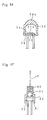
- FIG. 14 shows the optical electric integrated circuit according to a tenth embodiment of the optical device of this invention.
- This optical electric integrated circuit 51 comprises a substrate 54, a photodetecting region 52 and a signal processing circuit region 53 which are integrally molded of a transparent resin.
- GaAs doped by Er is crystal-grown as a buried light absorption layer 52a.
- a pair of electrodes 52b, 52b for taking out signals On the light absorption layer 52a there are formed a pair of electrodes 52b, 52b for taking out signals.
- the signal processing circuit 53 there are formed a contact region 53a and active layers 52b, 53b, and electrodes 53c, 53c, 53c thereon.
- the electrodes 53c, 53c, 53c are a source electrode, a gate electrode and a drain electrode, and function as circuit elements for signal processing to constitute a FET.
- a first ball lens 56 is adhered to the surface of the light absorption layer of the photodetecting region 52 so as to have an optical axis which coincides with an optical axis of an emission light from the light absorption layer 52. In thus adhered state the first ball lens 56 is buried in a molded resin 55.
- a second ball lens 57 is also buried in the resin molding before the first ball lens 56 so as to have an optical axis which coincides with an optical axis of an emitting light from the light absorption layer.
- the radiation from the outside is led from the entrance of the molded resin 55 to the second ball lens 57 to be condensed here and further condensed by the first ball lens 56 to focus on the surface of the light absorption layer 52.
- the radiation is photoelectrically converted and then is processed, e.g., amplified, etc. in the signal processing circuit region 53.
- the incident light is condensed on two stages by the first and the second ball lenses 56, 57, and consequently the optical electric integrated circuit can have very high condensation efficiency and can be compact.
Landscapes
- Physics & Mathematics (AREA)
- Engineering & Computer Science (AREA)
- Microelectronics & Electronic Packaging (AREA)
- General Physics & Mathematics (AREA)
- Optics & Photonics (AREA)
- Computer Hardware Design (AREA)
- Power Engineering (AREA)
- Manufacturing & Machinery (AREA)
- Condensed Matter Physics & Semiconductors (AREA)
- Electromagnetism (AREA)
- Led Device Packages (AREA)
- Optical Couplings Of Light Guides (AREA)
Claims (19)
- Eine optische Einrichtung, umfassend einen Rahmen (2), eine optische aktive Einrichtung (3), die auf dem Rahmen (2) angebracht und damit durch eine lichtübertragende Harzformung (4), in die die optisch aktive Einrichtung (3) vergraben ist, integriert ist, und zwei Linsen (8, 9), die in der lichtübertragenden Harzformung (4) auf eine aktive Oberfläche der optischen aktiven Einrichtung (3) hin gerichtet vergraben sind und die gleiche optische Achse (L) aufweisen, die senkrecht zu der Hauptoberfläche der optischen Einrichtung ist und mit einer optischen Achse eines einfallenden oder emittierenden Lichts der optischen aktiven Einrichtung (3) übereinstimmt.
- Optische Einrichtung nach Anspruch 1, dadurch gekennzeichnet, daß wenigstens eine Linse der Linsen durch Bondung an der aktiven Oberfläche der optischen aktiven Einrichtung gesichert ist.
- Optische Einrichtung nach Anspruch 1, dadurch gekennzeichnet, daß eine Einfalls- oder Emissionsoberfläche der Harzformung in konvexen Oberflächen, die als die Linsen dienen, ausgebildet ist.
- Optische Einrichtung, umfassend einen Rahmen (2), eine optische aktive Einrichtung (3), die auf dem Rahmen (2) angebracht und damit durch eine lichtübertragende Harzformung (4), in der die optische aktive Einrichtung vergraben ist, integriert ist, und zwei Linsen, die auf eine aktive Oberfläche der optischen Einrichtung (3) hin gerichtet positioniert sind und die gleiche optische Achse aufweisen, die senkrecht zu der aktiven Oberfläche ist und mit einer optischen Achse eines einfallenden oder emittierenden Lichts der optischen aktiven Einrichtung übereinstimmt, wobei eine der Linsen (4c, 4d) ein konvexer Linsenabschnitt ist, der integral auf einer Oberfläche der Harzformung gebildet ist, und die andere der Linsen eine sphärische Linse (8) ist, die in der Harzformung vergraben ist.
- Optische Einrichtung nach Anspruch 1 oder 4, dadurch gekennzeichnet, daß die Linsen sphärische Linsen sind.
- Optische Einrichtung nach Anspruch 5, dadurch gekennzeichnet, daß die Linsen Kugellinsen sind.
- Optische Einrichtung nach Anspruch 1, dadurch gekennzeichnet, daß die Linsen nicht-sphärische Linsen sind.
- Optische Einrichtung nach Anspruch 1, dadurch gekennzeichnet, daß Brechungsindizes der Linsen höher als der Brechungsindex der Harzformung sind.
- Optische Einrichtung nach Anspruch 1 oder 4, dadurch gekennzeichnet, daß die Linsen Glaslinsen sind.
- Optische Einrichtung nach Anspruch 9, dadurch gekennzeichnet, daß die Glaslinsen aus einem TiO2-Glas, einem BaO2-Glas oder einem SiO2-Glas als Hauptkomponenten gebildet sind.
- Optische Einrichtung nach Anspruch 1 oder 4, dadurch gekennzeichnet, daß die Linsen ein lichtübertragender Halbleiter sind.
- Optische Einrichtung nach Anspruch 11, dadurch gekennzeichnet, daß die optische Einrichtung InP oder GaAs als eine Hauptkomponente umfaßt.
- Optische Einrichtung nach Anspruch 3, dadurch gekennzeichnet, daß die Eintritts- und Austrittsoberfläche sphärisch sind.
- Optische Einrichtung nach Anspruch 4, dadurch gekennzeichnet, daß die Eintritts- und Austrittsoberfläche in gestuften Oberflächen als Fresnel-Linsen ausgebildet sind.
- Optische Einrichtung nach Anspruch 1, dadurch gekennzeichnet, daß ein Befestigungsflansch auf einem Teil der Harzformung gebildet ist.
- Optische Einrichtung nach Anspruch 1, dadurch gekennzeichnet, daß die optische aktive Einrichtung eine Leuchtdiode ist.
- Optische Einrichtung nach Anspruch 1, dadurch gekennzeichnet, daß die optische aktive Einrichtung eine fotodetektierende Einrichtung ist.
- Optische Einrichtung nach Anspruch 1, dadurch gekennzeichnet, daß die optische aktive Einrichtung eine optische elektrische integrierte Schaltung ist.
- Optische Einrichtung nach Anspruch 4, dadurch gekennzeichnet, daß die Brechungsindizes der Linsen höher als der Brechungsindex der Harzformung sind.
Applications Claiming Priority (14)
| Application Number | Priority Date | Filing Date | Title |
|---|---|---|---|
| JP88566/90 | 1990-04-03 | ||
| JP88568/90 | 1990-04-03 | ||
| JP2088567A JPH03286575A (ja) | 1990-04-03 | 1990-04-03 | 発光素子 |
| JP2088566A JPH03286574A (ja) | 1990-04-03 | 1990-04-03 | 発光素子 |
| JP2088568A JPH03286576A (ja) | 1990-04-03 | 1990-04-03 | 発光素子 |
| JP88567/90 | 1990-04-03 | ||
| JP2089892A JPH03288479A (ja) | 1990-04-04 | 1990-04-04 | 発光素子 |
| JP89892/90 | 1990-04-04 | ||
| JP2089891A JPH03288478A (ja) | 1990-04-04 | 1990-04-04 | 発光素子 |
| JP89893/90 | 1990-04-04 | ||
| JP89891/90 | 1990-04-04 | ||
| JP2089893A JPH03288480A (ja) | 1990-04-04 | 1990-04-04 | 発光素子 |
| JP246705/90 | 1990-09-17 | ||
| JP2246705A JPH04125979A (ja) | 1990-09-17 | 1990-09-17 | 発光素子 |
Publications (3)
| Publication Number | Publication Date |
|---|---|
| EP0450560A2 EP0450560A2 (de) | 1991-10-09 |
| EP0450560A3 EP0450560A3 (en) | 1992-05-20 |
| EP0450560B1 true EP0450560B1 (de) | 1998-07-22 |
Family
ID=27565456
Family Applications (1)
| Application Number | Title | Priority Date | Filing Date |
|---|---|---|---|
| EP91105169A Expired - Lifetime EP0450560B1 (de) | 1990-04-03 | 1991-04-02 | Optische Vorrichtung |
Country Status (3)
| Country | Link |
|---|---|
| US (1) | US5175783A (de) |
| EP (1) | EP0450560B1 (de) |
| DE (1) | DE69129817T2 (de) |
Families Citing this family (76)
| Publication number | Priority date | Publication date | Assignee | Title |
|---|---|---|---|---|
| US5327443A (en) * | 1991-10-30 | 1994-07-05 | Rohm Co., Ltd. | Package-type semiconductor laser device |
| EP0562754A1 (de) * | 1992-03-26 | 1993-09-29 | Hewlett-Packard Company | Optisches System für Laser |
| DE4311530A1 (de) * | 1992-10-02 | 1994-04-07 | Telefunken Microelectron | Optoelektronisches Bauelement mit engem Öffnungswinkel |
| US5311610A (en) * | 1993-03-31 | 1994-05-10 | Bell Communications Research, Inc. | Low-stress coupling of electrooptical device to optical fiber |
| US5337397A (en) * | 1993-06-07 | 1994-08-09 | Motorola, Inc. | Optical coupling device and method for making |
| US5642149A (en) * | 1993-09-20 | 1997-06-24 | Eastman Kodak Company | Apparatus and method for printing with a non-refractive imaging system |
| DE4413658A1 (de) * | 1994-04-20 | 1995-10-26 | Hoechst Ag | Verfahren zur Reinigung von Perfluoralkylbromiden oder Perfluoralkylendibromiden |
| US5638475A (en) * | 1995-10-06 | 1997-06-10 | Lucent Technologies Inc. | Apparatus for minimizing spherical aberration of light beam emitted into an optical fiber |
| US5808325A (en) * | 1996-06-28 | 1998-09-15 | Motorola, Inc. | Optical transmitter package assembly including lead frame having exposed flange with key |
| EP0826997B1 (de) * | 1996-08-26 | 2003-07-23 | Sumitomo Electric Industries, Ltd. | Optoelektronisches Modul und Verfahren zu dessen Herstellung |
| US5974066A (en) * | 1997-05-09 | 1999-10-26 | Motorola, Inc. | Low cost, efficient vertical cavity surface emitting laser package, method, bar code scanner and optical storage unit |
| WO1999000852A1 (fr) * | 1997-06-27 | 1999-01-07 | Iwasaki Electric Co., Ltd. | Diode electroluminescente de type reflechissante |
| TW357470B (en) * | 1997-07-15 | 1999-05-01 | Kai-Feng Huang | Vertical resonance cavity injection-type glowing laser package |
| US5940564A (en) * | 1997-08-05 | 1999-08-17 | Picolight, Inc. | Device for coupling a light source or receiver to an optical waveguide |
| JP3618534B2 (ja) * | 1997-11-28 | 2005-02-09 | 同和鉱業株式会社 | 光通信用ランプ装置とその製造方法 |
| US6086264A (en) * | 1997-12-16 | 2000-07-11 | Opto Power Corporation | Fiber-coupled laser device using square cross section fibers and method for fabrication |
| DE19841204A1 (de) * | 1998-09-09 | 2000-03-23 | Siemens Ag | Anordnung mit lichtemittierendem Leistungshalbleiterbauelement sowie Verfahren zur Herstellung derselben |
| DE19909242A1 (de) * | 1999-02-22 | 2000-08-31 | Siemens Ag | Verfahren und Gießform zum Herstellen eines elektrooptischen Moduls und elektrooptisches Modul |
| US6243508B1 (en) * | 1999-06-01 | 2001-06-05 | Picolight Incorporated | Electro-opto-mechanical assembly for coupling a light source or receiver to an optical waveguide |
| EP1113506A3 (de) * | 1999-12-28 | 2005-03-16 | Toyoda Gosei Co., Ltd. | Lichtemittierende Diode |
| DE10004411A1 (de) * | 2000-02-02 | 2001-08-16 | Infineon Technologies Ag | Elektrooptisches Sende-/Empfangsmodul und Verfahren zu seiner Herstellung |
| EP1146572A3 (de) | 2000-03-14 | 2005-03-23 | Toyoda Gosei Co., Ltd. | Lichtquellenvorrichtung |
| CN1186771C (zh) * | 2000-03-27 | 2005-01-26 | 皇家菲利浦电子有限公司 | 光扫描器、用于光扫描器的物镜系统及光播放器 |
| JP2003529107A (ja) * | 2000-03-27 | 2003-09-30 | コーニンクレッカ フィリップス エレクトロニクス エヌ ヴィ | 2個の1/2より大きい半球球面レンズを有する光学レンズ系 |
| DE10032839A1 (de) * | 2000-07-06 | 2002-02-21 | Osram Opto Semiconductors Gmbh | Bauelement und Verfahren zu dessen Herstellung |
| DE10053670A1 (de) * | 2000-10-28 | 2002-05-08 | Daimler Chrysler Ag | Optisches Signalübertragungssystem |
| US6607286B2 (en) | 2001-05-04 | 2003-08-19 | Lumileds Lighting, U.S., Llc | Lens and lens cap with sawtooth portion for light emitting diode |
| US6598998B2 (en) | 2001-05-04 | 2003-07-29 | Lumileds Lighting, U.S., Llc | Side emitting light emitting device |
| JP2002341193A (ja) * | 2001-05-15 | 2002-11-27 | Oki Electric Ind Co Ltd | 光学レンズ素子組立体 |
| US6886962B2 (en) * | 2001-06-27 | 2005-05-03 | Toyoda Gosei Co., Ltd. | Shielded reflective light-emitting diode |
| FR2832252B1 (fr) * | 2001-11-14 | 2004-03-12 | St Microelectronics Sa | Boitier semi-conducteur a capteur, muni d'un insert de fixation |
| US7102981B2 (en) * | 2001-12-05 | 2006-09-05 | Koninklijke Philips Electronics N.V. | Optical scanning device |
| FR2836236B1 (fr) * | 2002-02-21 | 2004-09-17 | Framatome Connectors Int | Dispositif de couplage optoelectronique perfectionne |
| US6826336B2 (en) * | 2002-05-22 | 2004-11-30 | The Boeing Company | Fiber optic LED illuminator |
| JP2004014803A (ja) * | 2002-06-06 | 2004-01-15 | Sumitomo Electric Ind Ltd | 光送信器及び光コネクタ |
| US6896381B2 (en) | 2002-10-11 | 2005-05-24 | Light Prescriptions Innovators, Llc | Compact folded-optics illumination lens |
| US6924943B2 (en) | 2002-12-02 | 2005-08-02 | Light Prescriptions Innovators, Llc | Asymmetric TIR lenses producing off-axis beams |
| DE10257128B3 (de) * | 2002-12-05 | 2004-05-27 | Schott Glas | Vorrichtung zur Einkopplung von Licht in einen Lichtleiter |
| US7254296B2 (en) * | 2003-01-16 | 2007-08-07 | Sae Magnetics (Hong Kong) Limited | Apparatus for improved fiber optic coupling efficiency |
| WO2004097477A2 (en) * | 2003-04-30 | 2004-11-11 | Tyco Electronics Raychem Nv | A connector device for coupling optical fibres, and method of production thereof |
| US7329029B2 (en) | 2003-05-13 | 2008-02-12 | Light Prescriptions Innovators, Llc | Optical device for LED-based lamp |
| US7021797B2 (en) | 2003-05-13 | 2006-04-04 | Light Prescriptions Innovators, Llc | Optical device for repositioning and redistributing an LED's light |
| US8075147B2 (en) | 2003-05-13 | 2011-12-13 | Light Prescriptions Innovators, Llc | Optical device for LED-based lamp |
| US7298942B2 (en) * | 2003-06-06 | 2007-11-20 | Finisar Corporation | Pluggable optical optic system having a lens fiber stop |
| US6803608B1 (en) * | 2003-06-10 | 2004-10-12 | Wen-Ching Chen | Light emitting diode used as an illuminant of an image sensor |
| EP1660918B1 (de) | 2003-07-29 | 2017-03-15 | Light Engine Limited | Umfänglich emittierende leuchtvorrichtungen und durch transversalachsen-profil-sweeps gebildete linsenelemente |
| US7502392B2 (en) | 2003-09-12 | 2009-03-10 | Semiconductor Energy Laboratory Co., Ltd. | Laser oscillator |
| WO2005045498A1 (en) * | 2003-11-10 | 2005-05-19 | Bookham Technology Plc | An optoelectric subassembly |
| JP4108597B2 (ja) * | 2003-12-24 | 2008-06-25 | 株式会社小糸製作所 | 車両用灯具ユニット |
| KR20060084256A (ko) * | 2005-01-19 | 2006-07-24 | 삼성전자주식회사 | 액정 표시 장치용 발광 다이오드 소자의 렌즈 조성물,이를 포함하는 발광 다이오드 소자, 백라이트 유닛 및액정 표시 장치 |
| EP1920285A4 (de) | 2005-07-28 | 2010-11-03 | Light Prescriptions Innovators | Linsenförmige optische freiformelemente und ihre anwendung auf kondensatoren und scheinwerfer |
| US8631787B2 (en) | 2005-07-28 | 2014-01-21 | Light Prescriptions Innovators, Llc | Multi-junction solar cells with a homogenizer system and coupled non-imaging light concentrator |
| WO2007014371A2 (en) | 2005-07-28 | 2007-02-01 | Light Prescriptions Innovators, Llc | Etendue-conserving illumination-optics for backlights and frontlights |
| JP2007178537A (ja) * | 2005-12-27 | 2007-07-12 | Fujifilm Corp | 光モジュールおよび光伝送システム |
| EP2064487A4 (de) | 2006-07-14 | 2010-09-01 | Light Prescriptions Innovators | Helligkeitsverstärkender film |
| WO2008022065A2 (en) | 2006-08-11 | 2008-02-21 | Light Prescriptions Innovators, Llc | Led luminance-enhancement and color-mixing by rotationally multiplexed beam-combining |
| JP2008122527A (ja) * | 2006-11-09 | 2008-05-29 | Nec Electronics Corp | 光トランシーバモジュールおよびその製造方法 |
| TWI396310B (zh) * | 2009-10-02 | 2013-05-11 | Everlight Electronics Co Ltd | 發光二極體結構 |
| US8923670B2 (en) | 2009-11-11 | 2014-12-30 | Samtec, Inc. | Molded optical structure for optical transceiver |
| WO2012011988A2 (en) * | 2010-04-20 | 2012-01-26 | The Johns Hopkins University | High-efficiency illumination system |
| WO2012005370A1 (en) * | 2010-07-07 | 2012-01-12 | Sumitomo Electric Industries, Ltd. | Optical module with a lens encapsulated within sealant and method for manufacturing the same |
| CN102971654B (zh) * | 2010-07-07 | 2014-12-24 | 住友电气工业株式会社 | 具有封装在密封体中的透镜的光学组件及其制造方法 |
| EP2613077A4 (de) * | 2010-08-31 | 2014-03-05 | Toshiba Lighting & Technology | Linse, beleuchtungssystem, birnenförmige lampe und beleuchtungsarmatur |
| US9537067B2 (en) * | 2012-05-03 | 2017-01-03 | Technische Universität Berlin | Radiation emitting device |
| JP6319318B2 (ja) | 2013-10-31 | 2018-05-09 | 住友電気工業株式会社 | 集光型太陽光発電ユニット、集光型太陽光発電モジュール、集光型太陽光発電パネル及び集光型太陽光発電装置 |
| WO2015146108A1 (ja) * | 2014-03-26 | 2015-10-01 | 日本電気株式会社 | 受光素子、光モジュール及び光受信器 |
| US9941965B2 (en) * | 2015-07-15 | 2018-04-10 | Flextronics Ap, Llc | Laser and optical charging and communications device and method of use |
| JP6789514B2 (ja) * | 2016-08-05 | 2020-11-25 | サンテック株式会社 | 検出装置 |
| US11049898B2 (en) | 2017-04-01 | 2021-06-29 | Ningbo Sunny Opotech Co., Ltd. | Systems and methods for manufacturing semiconductor modules |
| KR102334464B1 (ko) | 2017-04-12 | 2021-12-02 | 닝보 써니 오포테크 코., 엘티디. | 카메라 모듈, 이의 성형된 감광성 어셈블리 및 제조 방법, 그리고 전자 장치 |
| CN108535823A (zh) * | 2018-04-11 | 2018-09-14 | 中电科技集团重庆声光电有限公司 | 双透镜型管帽 |
| US10804305B2 (en) | 2018-04-23 | 2020-10-13 | Sunny Opotech North America Inc. | Manufacture of semiconductor module with dual molding |
| JP7399378B2 (ja) * | 2019-08-07 | 2023-12-18 | サターン ライセンシング エルエルシー | 光学装置、照明装置、表示装置および光通信装置 |
| JP7332895B2 (ja) | 2020-01-31 | 2023-08-24 | 日亜化学工業株式会社 | 面状光源の製造方法、面状光源、および光源 |
| JP7545038B2 (ja) * | 2020-09-25 | 2024-09-04 | 日亜化学工業株式会社 | 発光装置の製造方法 |
| CN113467015B (zh) * | 2021-08-03 | 2023-03-21 | 新疆师范大学 | 一种激光器耦合台的中心校准装置 |
Family Cites Families (24)
| Publication number | Priority date | Publication date | Assignee | Title |
|---|---|---|---|---|
| DE1539564A1 (de) * | 1966-11-09 | 1969-12-11 | Siemens Ag | Lumineszenzdiode mit hohem Wirkungsgrad |
| GB2026235B (en) * | 1978-06-06 | 1982-07-21 | Nippon Electric Co | Light emitting diode mounting structure for optical fibre communications |
| JPS5522709A (en) * | 1978-08-04 | 1980-02-18 | Fujitsu Ltd | Photo semiconductor element package |
| JPS55118681A (en) * | 1979-03-07 | 1980-09-11 | Marantz Japan Inc | Light emitting diode with reflecting mirror |
| DE2913262C2 (de) * | 1979-04-03 | 1982-04-29 | Kabelwerke Reinshagen Gmbh, 5600 Wuppertal | Elektro-optische Verbindungsvorrichtung |
| US4433898A (en) * | 1980-12-22 | 1984-02-28 | National Semiconductor Corporation | Fiber optic assembly for coupling an optical fiber and a light source |
| US4653847A (en) * | 1981-02-23 | 1987-03-31 | Motorola, Inc. | Fiber optics semiconductor package |
| WO1982004500A1 (en) * | 1981-06-12 | 1982-12-23 | Inc Motorola | Led having self-aligned lens |
| JPS5896783A (ja) * | 1981-12-04 | 1983-06-08 | Internatl Rectifier Corp Japan Ltd | 発光ダイオ−ド |
| JPS58111008A (ja) * | 1981-12-24 | 1983-07-01 | Toshiba Corp | 光モジユ−ル |
| US4699453A (en) * | 1982-11-24 | 1987-10-13 | Magnetic Controls Company | Monolithic fiber optic coupler having total internal reflecting surface |
| JPS6179269A (ja) * | 1984-09-26 | 1986-04-22 | Hitachi Micro Comput Eng Ltd | 光通信装置 |
| FR2581768B1 (fr) * | 1985-05-10 | 1987-09-04 | Thomson Csf | Composant optoelectrique bidirectionnel formant coupleur optique |
| US4705351A (en) * | 1985-11-26 | 1987-11-10 | Rca Corporation | Two lens optical package and method of making same |
| JPH0750797B2 (ja) * | 1985-12-13 | 1995-05-31 | 沖電気工業株式会社 | 発光ダイオ−ド |
| JPS6390866A (ja) * | 1986-10-03 | 1988-04-21 | Nec Corp | 半導体受光装置 |
| JPS63131586A (ja) * | 1986-11-21 | 1988-06-03 | Toshiba Corp | 半導体発光装置 |
| US4875750A (en) * | 1987-02-25 | 1989-10-24 | Siemens Aktiengesellschaft | Optoelectronic coupling element and method for its manufacture |
| JPS63300578A (ja) * | 1987-05-29 | 1988-12-07 | Nec Corp | 発光ダイオード |
| US4824201A (en) * | 1987-07-13 | 1989-04-25 | Bell Communications Research, Inc. | Simultaneous transmission of LED and laser signals over single mode fiber |
| US4946242A (en) * | 1987-08-28 | 1990-08-07 | Hitachi, Ltd. | Optical part including integral combination of optical fiber and light emitting or receiving element and method of manufacturing the same |
| US5074682A (en) * | 1988-03-02 | 1991-12-24 | Fujitsu Limited | Semiconductor laser module and positioning method thereof |
| JP2684219B2 (ja) * | 1989-07-05 | 1997-12-03 | 三菱電機株式会社 | 光半導体モジュール |
| US5093879A (en) * | 1990-06-22 | 1992-03-03 | International Business Machines Corporation | Electro-optical connectors |
-
1991
- 1991-04-02 EP EP91105169A patent/EP0450560B1/de not_active Expired - Lifetime
- 1991-04-02 DE DE69129817T patent/DE69129817T2/de not_active Expired - Fee Related
- 1991-04-03 US US07/680,236 patent/US5175783A/en not_active Expired - Lifetime
Also Published As
| Publication number | Publication date |
|---|---|
| US5175783A (en) | 1992-12-29 |
| EP0450560A2 (de) | 1991-10-09 |
| DE69129817T2 (de) | 1999-01-07 |
| EP0450560A3 (en) | 1992-05-20 |
| DE69129817D1 (de) | 1998-08-27 |
Similar Documents
| Publication | Publication Date | Title |
|---|---|---|
| EP0450560B1 (de) | Optische Vorrichtung | |
| US6900509B2 (en) | Optical receiver package | |
| US5546212A (en) | Optical module for two-way transmission | |
| US6250820B1 (en) | Electrooptical coupling component | |
| US4733094A (en) | Bidirectional optoelectronic component operating as an optical coupling device | |
| US7165896B2 (en) | Light transmitting modules with optical power monitoring | |
| US6567435B1 (en) | VCSEL power monitoring system using plastic encapsulation techniques | |
| US7128477B2 (en) | Optical transmitter and receiver module | |
| US5692083A (en) | In-line unitary optical device mount and package therefor | |
| US10754108B2 (en) | Optical subassembly, method for manufacturing optical subassembly, and optical module | |
| JP2006506657A (ja) | 光ファイバーとの半導体装置の能動的光学整合のための一体化プラットホーム | |
| US6097521A (en) | Optoelectronic module for bidirectional optical data transmission | |
| JPH10111439A (ja) | オプトエレクトロニクスモジュール | |
| US5105237A (en) | Semiconductor light-emitting device with partial encapsulation | |
| GB2312551A (en) | Encapsulating semiconductor optical devices | |
| US4741595A (en) | Optical transmission device | |
| JP3298798B2 (ja) | 光送受信モジュール | |
| US7290946B2 (en) | Optical subassembly | |
| USRE38280E1 (en) | Optoelectronic module for bidirectional optical data transmission | |
| KR100816063B1 (ko) | 수동 정렬된 광결합 장치 및 그 제작방법 | |
| JPH10253857A (ja) | 光通信モジュール | |
| US6879784B1 (en) | Bi-directional optical/electrical transceiver module | |
| JPH07168061A (ja) | 光送受信モジュール | |
| JPS6338272A (ja) | 光半導体装置 | |
| JP3452120B2 (ja) | 光モジュール及び光トランシーバ |
Legal Events
| Date | Code | Title | Description |
|---|---|---|---|
| PUAI | Public reference made under article 153(3) epc to a published international application that has entered the european phase |
Free format text: ORIGINAL CODE: 0009012 |
|
| AK | Designated contracting states |
Kind code of ref document: A2 Designated state(s): DE FR GB NL SE |
|
| 17P | Request for examination filed |
Effective date: 19911219 |
|
| PUAL | Search report despatched |
Free format text: ORIGINAL CODE: 0009013 |
|
| AK | Designated contracting states |
Kind code of ref document: A3 Designated state(s): DE FR GB NL SE |
|
| RIN1 | Information on inventor provided before grant (corrected) |
Inventor name: TATOH, NOBUYOSHI, C/O YOKOHAMA WORKS OF SUMITOMO |
|
| 17Q | First examination report despatched |
Effective date: 19950712 |
|
| GRAG | Despatch of communication of intention to grant |
Free format text: ORIGINAL CODE: EPIDOS AGRA |
|
| GRAG | Despatch of communication of intention to grant |
Free format text: ORIGINAL CODE: EPIDOS AGRA |
|
| GRAH | Despatch of communication of intention to grant a patent |
Free format text: ORIGINAL CODE: EPIDOS IGRA |
|
| GRAH | Despatch of communication of intention to grant a patent |
Free format text: ORIGINAL CODE: EPIDOS IGRA |
|
| GRAA | (expected) grant |
Free format text: ORIGINAL CODE: 0009210 |
|
| AK | Designated contracting states |
Kind code of ref document: B1 Designated state(s): DE FR GB NL SE |
|
| REF | Corresponds to: |
Ref document number: 69129817 Country of ref document: DE Date of ref document: 19980827 |
|
| ET | Fr: translation filed | ||
| PLBE | No opposition filed within time limit |
Free format text: ORIGINAL CODE: 0009261 |
|
| STAA | Information on the status of an ep patent application or granted ep patent |
Free format text: STATUS: NO OPPOSITION FILED WITHIN TIME LIMIT |
|
| 26N | No opposition filed | ||
| REG | Reference to a national code |
Ref country code: GB Ref legal event code: IF02 |
|
| PGFP | Annual fee paid to national office [announced via postgrant information from national office to epo] |
Ref country code: GB Payment date: 20030402 Year of fee payment: 13 |
|
| PGFP | Annual fee paid to national office [announced via postgrant information from national office to epo] |
Ref country code: SE Payment date: 20030404 Year of fee payment: 13 |
|
| PGFP | Annual fee paid to national office [announced via postgrant information from national office to epo] |
Ref country code: FR Payment date: 20030408 Year of fee payment: 13 |
|
| PGFP | Annual fee paid to national office [announced via postgrant information from national office to epo] |
Ref country code: DE Payment date: 20030409 Year of fee payment: 13 |
|
| PGFP | Annual fee paid to national office [announced via postgrant information from national office to epo] |
Ref country code: NL Payment date: 20030429 Year of fee payment: 13 |
|
| PG25 | Lapsed in a contracting state [announced via postgrant information from national office to epo] |
Ref country code: GB Free format text: LAPSE BECAUSE OF NON-PAYMENT OF DUE FEES Effective date: 20040402 |
|
| PG25 | Lapsed in a contracting state [announced via postgrant information from national office to epo] |
Ref country code: SE Free format text: LAPSE BECAUSE OF NON-PAYMENT OF DUE FEES Effective date: 20040403 |
|
| PG25 | Lapsed in a contracting state [announced via postgrant information from national office to epo] |
Ref country code: NL Free format text: LAPSE BECAUSE OF NON-PAYMENT OF DUE FEES Effective date: 20041101 |
|
| PG25 | Lapsed in a contracting state [announced via postgrant information from national office to epo] |
Ref country code: DE Free format text: LAPSE BECAUSE OF NON-PAYMENT OF DUE FEES Effective date: 20041103 |
|
| GBPC | Gb: european patent ceased through non-payment of renewal fee | ||
| EUG | Se: european patent has lapsed | ||
| PG25 | Lapsed in a contracting state [announced via postgrant information from national office to epo] |
Ref country code: FR Free format text: LAPSE BECAUSE OF NON-PAYMENT OF DUE FEES Effective date: 20041231 |
|
| NLV4 | Nl: lapsed or anulled due to non-payment of the annual fee |
Effective date: 20041101 |
|
| REG | Reference to a national code |
Ref country code: FR Ref legal event code: ST |