EP0430255A2 - Adhésif conducteur et article fabriqué avec celui-ci - Google Patents
Adhésif conducteur et article fabriqué avec celui-ci Download PDFInfo
- Publication number
- EP0430255A2 EP0430255A2 EP90122877A EP90122877A EP0430255A2 EP 0430255 A2 EP0430255 A2 EP 0430255A2 EP 90122877 A EP90122877 A EP 90122877A EP 90122877 A EP90122877 A EP 90122877A EP 0430255 A2 EP0430255 A2 EP 0430255A2
- Authority
- EP
- European Patent Office
- Prior art keywords
- conductive
- conductive adhesive
- weight
- molecular
- parts
- Prior art date
- Legal status (The legal status is an assumption and is not a legal conclusion. Google has not performed a legal analysis and makes no representation as to the accuracy of the status listed.)
- Granted
Links
- 239000000853 adhesive Substances 0.000 title claims abstract description 48
- 230000001070 adhesive effect Effects 0.000 title claims abstract description 48
- 239000004065 semiconductor Substances 0.000 claims abstract description 64
- 239000008188 pellet Substances 0.000 claims abstract description 45
- KPUWHANPEXNPJT-UHFFFAOYSA-N disiloxane Chemical class [SiH3]O[SiH3] KPUWHANPEXNPJT-UHFFFAOYSA-N 0.000 claims abstract description 41
- 239000000203 mixture Substances 0.000 claims abstract description 34
- 229920002379 silicone rubber Polymers 0.000 claims abstract description 28
- 239000004945 silicone rubber Substances 0.000 claims abstract description 28
- 229910052751 metal Inorganic materials 0.000 claims abstract description 7
- 239000002184 metal Substances 0.000 claims abstract description 7
- 229920001296 polysiloxane Polymers 0.000 claims description 23
- VYPSYNLAJGMNEJ-UHFFFAOYSA-N Silicium dioxide Chemical compound O=[Si]=O VYPSYNLAJGMNEJ-UHFFFAOYSA-N 0.000 claims description 18
- 125000003342 alkenyl group Chemical group 0.000 claims description 12
- 125000004435 hydrogen atom Chemical group [H]* 0.000 claims description 10
- 239000003054 catalyst Substances 0.000 claims description 9
- 239000011231 conductive filler Substances 0.000 claims description 7
- 239000000377 silicon dioxide Substances 0.000 claims description 7
- 239000000945 filler Substances 0.000 claims description 5
- 150000003961 organosilicon compounds Chemical class 0.000 claims description 5
- 125000001183 hydrocarbyl group Chemical group 0.000 claims description 4
- 238000004519 manufacturing process Methods 0.000 claims description 4
- 229920006136 organohydrogenpolysiloxane Polymers 0.000 claims description 4
- 125000000524 functional group Chemical group 0.000 claims description 3
- 230000003197 catalytic effect Effects 0.000 claims description 2
- BQCADISMDOOEFD-UHFFFAOYSA-N Silver Chemical compound [Ag] BQCADISMDOOEFD-UHFFFAOYSA-N 0.000 abstract description 16
- RYGMFSIKBFXOCR-UHFFFAOYSA-N Copper Chemical compound [Cu] RYGMFSIKBFXOCR-UHFFFAOYSA-N 0.000 abstract description 14
- 229910052802 copper Inorganic materials 0.000 abstract description 14
- 239000010949 copper Substances 0.000 abstract description 14
- PCHJSUWPFVWCPO-UHFFFAOYSA-N gold Chemical compound [Au] PCHJSUWPFVWCPO-UHFFFAOYSA-N 0.000 abstract description 11
- 229910052737 gold Inorganic materials 0.000 abstract description 10
- 239000010931 gold Substances 0.000 abstract description 10
- PXHVJJICTQNCMI-UHFFFAOYSA-N Nickel Chemical compound [Ni] PXHVJJICTQNCMI-UHFFFAOYSA-N 0.000 abstract description 6
- 229910052709 silver Inorganic materials 0.000 abstract description 5
- 239000004332 silver Substances 0.000 abstract description 5
- 229910052759 nickel Inorganic materials 0.000 abstract description 3
- 235000013870 dimethyl polysiloxane Nutrition 0.000 description 19
- 229920000435 poly(dimethylsiloxane) Polymers 0.000 description 19
- 239000004205 dimethyl polysiloxane Substances 0.000 description 18
- -1 tab Substances 0.000 description 17
- LFQSCWFLJHTTHZ-UHFFFAOYSA-N Ethanol Chemical compound CCO LFQSCWFLJHTTHZ-UHFFFAOYSA-N 0.000 description 13
- 125000000391 vinyl group Chemical group [H]C([*])=C([H])[H] 0.000 description 13
- 238000005336 cracking Methods 0.000 description 9
- BASFCYQUMIYNBI-UHFFFAOYSA-N platinum Chemical compound [Pt] BASFCYQUMIYNBI-UHFFFAOYSA-N 0.000 description 9
- 239000011347 resin Substances 0.000 description 9
- 229920005989 resin Polymers 0.000 description 9
- 239000002253 acid Substances 0.000 description 7
- 238000004817 gas chromatography Methods 0.000 description 6
- 238000000034 method Methods 0.000 description 6
- 125000002496 methyl group Chemical group [H]C([H])([H])* 0.000 description 6
- 229920002554 vinyl polymer Polymers 0.000 description 6
- 230000002950 deficient Effects 0.000 description 5
- 239000003822 epoxy resin Substances 0.000 description 5
- 229920000647 polyepoxide Polymers 0.000 description 5
- 239000000565 sealant Substances 0.000 description 5
- CSCPPACGZOOCGX-UHFFFAOYSA-N Acetone Chemical compound CC(C)=O CSCPPACGZOOCGX-UHFFFAOYSA-N 0.000 description 4
- 239000002245 particle Substances 0.000 description 4
- 229910052697 platinum Inorganic materials 0.000 description 4
- OKKJLVBELUTLKV-UHFFFAOYSA-N Methanol Chemical compound OC OKKJLVBELUTLKV-UHFFFAOYSA-N 0.000 description 3
- 150000001336 alkenes Chemical class 0.000 description 3
- 229910052782 aluminium Inorganic materials 0.000 description 3
- 125000004122 cyclic group Chemical group 0.000 description 3
- 230000007547 defect Effects 0.000 description 3
- 238000010438 heat treatment Methods 0.000 description 3
- 239000000463 material Substances 0.000 description 3
- JRZJOMJEPLMPRA-UHFFFAOYSA-N olefin Natural products CCCCCCCC=C JRZJOMJEPLMPRA-UHFFFAOYSA-N 0.000 description 3
- RTZKZFJDLAIYFH-UHFFFAOYSA-N Diethyl ether Chemical compound CCOCC RTZKZFJDLAIYFH-UHFFFAOYSA-N 0.000 description 2
- LRHPLDYGYMQRHN-UHFFFAOYSA-N N-Butanol Chemical compound CCCCO LRHPLDYGYMQRHN-UHFFFAOYSA-N 0.000 description 2
- XUIMIQQOPSSXEZ-UHFFFAOYSA-N Silicon Chemical compound [Si] XUIMIQQOPSSXEZ-UHFFFAOYSA-N 0.000 description 2
- QAOWNCQODCNURD-UHFFFAOYSA-N Sulfuric acid Chemical compound OS(O)(=O)=O QAOWNCQODCNURD-UHFFFAOYSA-N 0.000 description 2
- 239000007767 bonding agent Substances 0.000 description 2
- 239000006227 byproduct Substances 0.000 description 2
- 239000007809 chemical reaction catalyst Substances 0.000 description 2
- 230000007423 decrease Effects 0.000 description 2
- 238000002481 ethanol extraction Methods 0.000 description 2
- 125000001495 ethyl group Chemical group [H]C([H])([H])C([H])([H])* 0.000 description 2
- 238000011156 evaluation Methods 0.000 description 2
- 239000007789 gas Substances 0.000 description 2
- 238000006459 hydrosilylation reaction Methods 0.000 description 2
- 238000005259 measurement Methods 0.000 description 2
- 238000006386 neutralization reaction Methods 0.000 description 2
- 229920001721 polyimide Polymers 0.000 description 2
- 239000009719 polyimide resin Substances 0.000 description 2
- 125000004368 propenyl group Chemical group C(=CC)* 0.000 description 2
- 125000001436 propyl group Chemical group [H]C([*])([H])C([H])([H])C([H])([H])[H] 0.000 description 2
- 238000007789 sealing Methods 0.000 description 2
- 229910052710 silicon Inorganic materials 0.000 description 2
- 239000010703 silicon Substances 0.000 description 2
- 235000012239 silicon dioxide Nutrition 0.000 description 2
- 239000002904 solvent Substances 0.000 description 2
- 125000003903 2-propenyl group Chemical group [H]C([*])([H])C([H])=C([H])[H] 0.000 description 1
- 239000004215 Carbon black (E152) Substances 0.000 description 1
- 239000004971 Cross linker Substances 0.000 description 1
- 229910000881 Cu alloy Inorganic materials 0.000 description 1
- 229910003271 Ni-Fe Inorganic materials 0.000 description 1
- 229910007161 Si(CH3)3 Inorganic materials 0.000 description 1
- 229910020388 SiO1/2 Inorganic materials 0.000 description 1
- 238000007259 addition reaction Methods 0.000 description 1
- 239000002318 adhesion promoter Substances 0.000 description 1
- 125000000217 alkyl group Chemical group 0.000 description 1
- 229910045601 alloy Inorganic materials 0.000 description 1
- 239000000956 alloy Substances 0.000 description 1
- PNEYBMLMFCGWSK-UHFFFAOYSA-N aluminium oxide Inorganic materials [O-2].[O-2].[O-2].[Al+3].[Al+3] PNEYBMLMFCGWSK-UHFFFAOYSA-N 0.000 description 1
- 125000003118 aryl group Chemical group 0.000 description 1
- 238000005452 bending Methods 0.000 description 1
- 239000000919 ceramic Substances 0.000 description 1
- 238000006243 chemical reaction Methods 0.000 description 1
- 238000004587 chromatography analysis Methods 0.000 description 1
- 238000001816 cooling Methods 0.000 description 1
- 229920001577 copolymer Polymers 0.000 description 1
- 229910002026 crystalline silica Inorganic materials 0.000 description 1
- 239000000539 dimer Substances 0.000 description 1
- 239000002031 ethanolic fraction Substances 0.000 description 1
- 238000000605 extraction Methods 0.000 description 1
- 229910021485 fumed silica Inorganic materials 0.000 description 1
- 239000011521 glass Substances 0.000 description 1
- 125000006038 hexenyl group Chemical group 0.000 description 1
- 229930195733 hydrocarbon Natural products 0.000 description 1
- 150000002430 hydrocarbons Chemical class 0.000 description 1
- 230000005764 inhibitory process Effects 0.000 description 1
- 230000010354 integration Effects 0.000 description 1
- 150000002576 ketones Chemical class 0.000 description 1
- 150000002739 metals Chemical class 0.000 description 1
- 238000002156 mixing Methods 0.000 description 1
- 238000012986 modification Methods 0.000 description 1
- 230000004048 modification Effects 0.000 description 1
- 238000000199 molecular distillation Methods 0.000 description 1
- 239000003960 organic solvent Substances 0.000 description 1
- 125000001997 phenyl group Chemical group [H]C1=C([H])C([H])=C(*)C([H])=C1[H] 0.000 description 1
- 150000003057 platinum Chemical class 0.000 description 1
- IALUUOKJPBOFJL-UHFFFAOYSA-N potassium oxidosilane Chemical compound [K+].[SiH3][O-] IALUUOKJPBOFJL-UHFFFAOYSA-N 0.000 description 1
- 239000000047 product Substances 0.000 description 1
- BDERNNFJNOPAEC-UHFFFAOYSA-N propan-1-ol Chemical compound CCCO BDERNNFJNOPAEC-UHFFFAOYSA-N 0.000 description 1
- 239000010453 quartz Substances 0.000 description 1
- 238000011160 research Methods 0.000 description 1
- 229920006395 saturated elastomer Polymers 0.000 description 1
- 239000007787 solid Substances 0.000 description 1
- 239000011949 solid catalyst Substances 0.000 description 1
- 239000010409 thin film Substances 0.000 description 1
- 125000003944 tolyl group Chemical group 0.000 description 1
- 238000010792 warming Methods 0.000 description 1
Images
Classifications
-
- H—ELECTRICITY
- H01—ELECTRIC ELEMENTS
- H01L—SEMICONDUCTOR DEVICES NOT COVERED BY CLASS H10
- H01L24/00—Arrangements for connecting or disconnecting semiconductor or solid-state bodies; Methods or apparatus related thereto
- H01L24/80—Methods for connecting semiconductor or other solid state bodies using means for bonding being attached to, or being formed on, the surface to be connected
- H01L24/83—Methods for connecting semiconductor or other solid state bodies using means for bonding being attached to, or being formed on, the surface to be connected using a layer connector
-
- C—CHEMISTRY; METALLURGY
- C09—DYES; PAINTS; POLISHES; NATURAL RESINS; ADHESIVES; COMPOSITIONS NOT OTHERWISE PROVIDED FOR; APPLICATIONS OF MATERIALS NOT OTHERWISE PROVIDED FOR
- C09J—ADHESIVES; NON-MECHANICAL ASPECTS OF ADHESIVE PROCESSES IN GENERAL; ADHESIVE PROCESSES NOT PROVIDED FOR ELSEWHERE; USE OF MATERIALS AS ADHESIVES
- C09J183/00—Adhesives based on macromolecular compounds obtained by reactions forming in the main chain of the macromolecule a linkage containing silicon, with or without sulfur, nitrogen, oxygen, or carbon only; Adhesives based on derivatives of such polymers
- C09J183/04—Polysiloxanes
-
- H—ELECTRICITY
- H01—ELECTRIC ELEMENTS
- H01L—SEMICONDUCTOR DEVICES NOT COVERED BY CLASS H10
- H01L23/00—Details of semiconductor or other solid state devices
- H01L23/48—Arrangements for conducting electric current to or from the solid state body in operation, e.g. leads, terminal arrangements ; Selection of materials therefor
- H01L23/488—Arrangements for conducting electric current to or from the solid state body in operation, e.g. leads, terminal arrangements ; Selection of materials therefor consisting of soldered or bonded constructions
- H01L23/495—Lead-frames or other flat leads
- H01L23/49503—Lead-frames or other flat leads characterised by the die pad
- H01L23/49513—Lead-frames or other flat leads characterised by the die pad having bonding material between chip and die pad
-
- H—ELECTRICITY
- H01—ELECTRIC ELEMENTS
- H01L—SEMICONDUCTOR DEVICES NOT COVERED BY CLASS H10
- H01L24/00—Arrangements for connecting or disconnecting semiconductor or solid-state bodies; Methods or apparatus related thereto
- H01L24/01—Means for bonding being attached to, or being formed on, the surface to be connected, e.g. chip-to-package, die-attach, "first-level" interconnects; Manufacturing methods related thereto
- H01L24/26—Layer connectors, e.g. plate connectors, solder or adhesive layers; Manufacturing methods related thereto
- H01L24/28—Structure, shape, material or disposition of the layer connectors prior to the connecting process
- H01L24/29—Structure, shape, material or disposition of the layer connectors prior to the connecting process of an individual layer connector
-
- H—ELECTRICITY
- H01—ELECTRIC ELEMENTS
- H01L—SEMICONDUCTOR DEVICES NOT COVERED BY CLASS H10
- H01L24/00—Arrangements for connecting or disconnecting semiconductor or solid-state bodies; Methods or apparatus related thereto
- H01L24/01—Means for bonding being attached to, or being formed on, the surface to be connected, e.g. chip-to-package, die-attach, "first-level" interconnects; Manufacturing methods related thereto
- H01L24/26—Layer connectors, e.g. plate connectors, solder or adhesive layers; Manufacturing methods related thereto
- H01L24/31—Structure, shape, material or disposition of the layer connectors after the connecting process
- H01L24/32—Structure, shape, material or disposition of the layer connectors after the connecting process of an individual layer connector
-
- H—ELECTRICITY
- H01—ELECTRIC ELEMENTS
- H01L—SEMICONDUCTOR DEVICES NOT COVERED BY CLASS H10
- H01L2224/00—Indexing scheme for arrangements for connecting or disconnecting semiconductor or solid-state bodies and methods related thereto as covered by H01L24/00
- H01L2224/01—Means for bonding being attached to, or being formed on, the surface to be connected, e.g. chip-to-package, die-attach, "first-level" interconnects; Manufacturing methods related thereto
- H01L2224/02—Bonding areas; Manufacturing methods related thereto
- H01L2224/04—Structure, shape, material or disposition of the bonding areas prior to the connecting process
- H01L2224/05—Structure, shape, material or disposition of the bonding areas prior to the connecting process of an individual bonding area
- H01L2224/0554—External layer
- H01L2224/05599—Material
- H01L2224/056—Material with a principal constituent of the material being a metal or a metalloid, e.g. boron [B], silicon [Si], germanium [Ge], arsenic [As], antimony [Sb], tellurium [Te] and polonium [Po], and alloys thereof
- H01L2224/05617—Material with a principal constituent of the material being a metal or a metalloid, e.g. boron [B], silicon [Si], germanium [Ge], arsenic [As], antimony [Sb], tellurium [Te] and polonium [Po], and alloys thereof the principal constituent melting at a temperature of greater than or equal to 400°C and less than 950°C
- H01L2224/05624—Aluminium [Al] as principal constituent
-
- H—ELECTRICITY
- H01—ELECTRIC ELEMENTS
- H01L—SEMICONDUCTOR DEVICES NOT COVERED BY CLASS H10
- H01L2224/00—Indexing scheme for arrangements for connecting or disconnecting semiconductor or solid-state bodies and methods related thereto as covered by H01L24/00
- H01L2224/01—Means for bonding being attached to, or being formed on, the surface to be connected, e.g. chip-to-package, die-attach, "first-level" interconnects; Manufacturing methods related thereto
- H01L2224/26—Layer connectors, e.g. plate connectors, solder or adhesive layers; Manufacturing methods related thereto
- H01L2224/28—Structure, shape, material or disposition of the layer connectors prior to the connecting process
- H01L2224/29—Structure, shape, material or disposition of the layer connectors prior to the connecting process of an individual layer connector
- H01L2224/29001—Core members of the layer connector
- H01L2224/29099—Material
- H01L2224/2919—Material with a principal constituent of the material being a polymer, e.g. polyester, phenolic based polymer, epoxy
- H01L2224/29191—The principal constituent being an elastomer, e.g. silicones, isoprene, neoprene
-
- H—ELECTRICITY
- H01—ELECTRIC ELEMENTS
- H01L—SEMICONDUCTOR DEVICES NOT COVERED BY CLASS H10
- H01L2224/00—Indexing scheme for arrangements for connecting or disconnecting semiconductor or solid-state bodies and methods related thereto as covered by H01L24/00
- H01L2224/01—Means for bonding being attached to, or being formed on, the surface to be connected, e.g. chip-to-package, die-attach, "first-level" interconnects; Manufacturing methods related thereto
- H01L2224/26—Layer connectors, e.g. plate connectors, solder or adhesive layers; Manufacturing methods related thereto
- H01L2224/28—Structure, shape, material or disposition of the layer connectors prior to the connecting process
- H01L2224/29—Structure, shape, material or disposition of the layer connectors prior to the connecting process of an individual layer connector
- H01L2224/29001—Core members of the layer connector
- H01L2224/29099—Material
- H01L2224/29198—Material with a principal constituent of the material being a combination of two or more materials in the form of a matrix with a filler, i.e. being a hybrid material, e.g. segmented structures, foams
- H01L2224/29199—Material of the matrix
- H01L2224/2929—Material of the matrix with a principal constituent of the material being a polymer, e.g. polyester, phenolic based polymer, epoxy
-
- H—ELECTRICITY
- H01—ELECTRIC ELEMENTS
- H01L—SEMICONDUCTOR DEVICES NOT COVERED BY CLASS H10
- H01L2224/00—Indexing scheme for arrangements for connecting or disconnecting semiconductor or solid-state bodies and methods related thereto as covered by H01L24/00
- H01L2224/01—Means for bonding being attached to, or being formed on, the surface to be connected, e.g. chip-to-package, die-attach, "first-level" interconnects; Manufacturing methods related thereto
- H01L2224/26—Layer connectors, e.g. plate connectors, solder or adhesive layers; Manufacturing methods related thereto
- H01L2224/28—Structure, shape, material or disposition of the layer connectors prior to the connecting process
- H01L2224/29—Structure, shape, material or disposition of the layer connectors prior to the connecting process of an individual layer connector
- H01L2224/29001—Core members of the layer connector
- H01L2224/29099—Material
- H01L2224/29198—Material with a principal constituent of the material being a combination of two or more materials in the form of a matrix with a filler, i.e. being a hybrid material, e.g. segmented structures, foams
- H01L2224/29298—Fillers
- H01L2224/29299—Base material
- H01L2224/293—Base material with a principal constituent of the material being a metal or a metalloid, e.g. boron [B], silicon [Si], germanium [Ge], arsenic [As], antimony [Sb], tellurium [Te] and polonium [Po], and alloys thereof
- H01L2224/29338—Base material with a principal constituent of the material being a metal or a metalloid, e.g. boron [B], silicon [Si], germanium [Ge], arsenic [As], antimony [Sb], tellurium [Te] and polonium [Po], and alloys thereof the principal constituent melting at a temperature of greater than or equal to 950°C and less than 1550°C
- H01L2224/29339—Silver [Ag] as principal constituent
-
- H—ELECTRICITY
- H01—ELECTRIC ELEMENTS
- H01L—SEMICONDUCTOR DEVICES NOT COVERED BY CLASS H10
- H01L2224/00—Indexing scheme for arrangements for connecting or disconnecting semiconductor or solid-state bodies and methods related thereto as covered by H01L24/00
- H01L2224/01—Means for bonding being attached to, or being formed on, the surface to be connected, e.g. chip-to-package, die-attach, "first-level" interconnects; Manufacturing methods related thereto
- H01L2224/26—Layer connectors, e.g. plate connectors, solder or adhesive layers; Manufacturing methods related thereto
- H01L2224/28—Structure, shape, material or disposition of the layer connectors prior to the connecting process
- H01L2224/29—Structure, shape, material or disposition of the layer connectors prior to the connecting process of an individual layer connector
- H01L2224/29001—Core members of the layer connector
- H01L2224/29099—Material
- H01L2224/29198—Material with a principal constituent of the material being a combination of two or more materials in the form of a matrix with a filler, i.e. being a hybrid material, e.g. segmented structures, foams
- H01L2224/29298—Fillers
- H01L2224/29299—Base material
- H01L2224/293—Base material with a principal constituent of the material being a metal or a metalloid, e.g. boron [B], silicon [Si], germanium [Ge], arsenic [As], antimony [Sb], tellurium [Te] and polonium [Po], and alloys thereof
- H01L2224/29338—Base material with a principal constituent of the material being a metal or a metalloid, e.g. boron [B], silicon [Si], germanium [Ge], arsenic [As], antimony [Sb], tellurium [Te] and polonium [Po], and alloys thereof the principal constituent melting at a temperature of greater than or equal to 950°C and less than 1550°C
- H01L2224/29344—Gold [Au] as principal constituent
-
- H—ELECTRICITY
- H01—ELECTRIC ELEMENTS
- H01L—SEMICONDUCTOR DEVICES NOT COVERED BY CLASS H10
- H01L2224/00—Indexing scheme for arrangements for connecting or disconnecting semiconductor or solid-state bodies and methods related thereto as covered by H01L24/00
- H01L2224/01—Means for bonding being attached to, or being formed on, the surface to be connected, e.g. chip-to-package, die-attach, "first-level" interconnects; Manufacturing methods related thereto
- H01L2224/26—Layer connectors, e.g. plate connectors, solder or adhesive layers; Manufacturing methods related thereto
- H01L2224/28—Structure, shape, material or disposition of the layer connectors prior to the connecting process
- H01L2224/29—Structure, shape, material or disposition of the layer connectors prior to the connecting process of an individual layer connector
- H01L2224/29001—Core members of the layer connector
- H01L2224/29099—Material
- H01L2224/29198—Material with a principal constituent of the material being a combination of two or more materials in the form of a matrix with a filler, i.e. being a hybrid material, e.g. segmented structures, foams
- H01L2224/29298—Fillers
- H01L2224/29299—Base material
- H01L2224/293—Base material with a principal constituent of the material being a metal or a metalloid, e.g. boron [B], silicon [Si], germanium [Ge], arsenic [As], antimony [Sb], tellurium [Te] and polonium [Po], and alloys thereof
- H01L2224/29338—Base material with a principal constituent of the material being a metal or a metalloid, e.g. boron [B], silicon [Si], germanium [Ge], arsenic [As], antimony [Sb], tellurium [Te] and polonium [Po], and alloys thereof the principal constituent melting at a temperature of greater than or equal to 950°C and less than 1550°C
- H01L2224/29347—Copper [Cu] as principal constituent
-
- H—ELECTRICITY
- H01—ELECTRIC ELEMENTS
- H01L—SEMICONDUCTOR DEVICES NOT COVERED BY CLASS H10
- H01L2224/00—Indexing scheme for arrangements for connecting or disconnecting semiconductor or solid-state bodies and methods related thereto as covered by H01L24/00
- H01L2224/01—Means for bonding being attached to, or being formed on, the surface to be connected, e.g. chip-to-package, die-attach, "first-level" interconnects; Manufacturing methods related thereto
- H01L2224/26—Layer connectors, e.g. plate connectors, solder or adhesive layers; Manufacturing methods related thereto
- H01L2224/28—Structure, shape, material or disposition of the layer connectors prior to the connecting process
- H01L2224/29—Structure, shape, material or disposition of the layer connectors prior to the connecting process of an individual layer connector
- H01L2224/29001—Core members of the layer connector
- H01L2224/29099—Material
- H01L2224/29198—Material with a principal constituent of the material being a combination of two or more materials in the form of a matrix with a filler, i.e. being a hybrid material, e.g. segmented structures, foams
- H01L2224/29298—Fillers
- H01L2224/29299—Base material
- H01L2224/293—Base material with a principal constituent of the material being a metal or a metalloid, e.g. boron [B], silicon [Si], germanium [Ge], arsenic [As], antimony [Sb], tellurium [Te] and polonium [Po], and alloys thereof
- H01L2224/29338—Base material with a principal constituent of the material being a metal or a metalloid, e.g. boron [B], silicon [Si], germanium [Ge], arsenic [As], antimony [Sb], tellurium [Te] and polonium [Po], and alloys thereof the principal constituent melting at a temperature of greater than or equal to 950°C and less than 1550°C
- H01L2224/29355—Nickel [Ni] as principal constituent
-
- H—ELECTRICITY
- H01—ELECTRIC ELEMENTS
- H01L—SEMICONDUCTOR DEVICES NOT COVERED BY CLASS H10
- H01L2224/00—Indexing scheme for arrangements for connecting or disconnecting semiconductor or solid-state bodies and methods related thereto as covered by H01L24/00
- H01L2224/01—Means for bonding being attached to, or being formed on, the surface to be connected, e.g. chip-to-package, die-attach, "first-level" interconnects; Manufacturing methods related thereto
- H01L2224/26—Layer connectors, e.g. plate connectors, solder or adhesive layers; Manufacturing methods related thereto
- H01L2224/31—Structure, shape, material or disposition of the layer connectors after the connecting process
- H01L2224/32—Structure, shape, material or disposition of the layer connectors after the connecting process of an individual layer connector
- H01L2224/321—Disposition
- H01L2224/32151—Disposition the layer connector connecting between a semiconductor or solid-state body and an item not being a semiconductor or solid-state body, e.g. chip-to-substrate, chip-to-passive
- H01L2224/32221—Disposition the layer connector connecting between a semiconductor or solid-state body and an item not being a semiconductor or solid-state body, e.g. chip-to-substrate, chip-to-passive the body and the item being stacked
- H01L2224/32245—Disposition the layer connector connecting between a semiconductor or solid-state body and an item not being a semiconductor or solid-state body, e.g. chip-to-substrate, chip-to-passive the body and the item being stacked the item being metallic
-
- H—ELECTRICITY
- H01—ELECTRIC ELEMENTS
- H01L—SEMICONDUCTOR DEVICES NOT COVERED BY CLASS H10
- H01L2224/00—Indexing scheme for arrangements for connecting or disconnecting semiconductor or solid-state bodies and methods related thereto as covered by H01L24/00
- H01L2224/01—Means for bonding being attached to, or being formed on, the surface to be connected, e.g. chip-to-package, die-attach, "first-level" interconnects; Manufacturing methods related thereto
- H01L2224/42—Wire connectors; Manufacturing methods related thereto
- H01L2224/44—Structure, shape, material or disposition of the wire connectors prior to the connecting process
- H01L2224/45—Structure, shape, material or disposition of the wire connectors prior to the connecting process of an individual wire connector
- H01L2224/45001—Core members of the connector
- H01L2224/45099—Material
- H01L2224/451—Material with a principal constituent of the material being a metal or a metalloid, e.g. boron (B), silicon (Si), germanium (Ge), arsenic (As), antimony (Sb), tellurium (Te) and polonium (Po), and alloys thereof
- H01L2224/45138—Material with a principal constituent of the material being a metal or a metalloid, e.g. boron (B), silicon (Si), germanium (Ge), arsenic (As), antimony (Sb), tellurium (Te) and polonium (Po), and alloys thereof the principal constituent melting at a temperature of greater than or equal to 950°C and less than 1550°C
- H01L2224/45144—Gold (Au) as principal constituent
-
- H—ELECTRICITY
- H01—ELECTRIC ELEMENTS
- H01L—SEMICONDUCTOR DEVICES NOT COVERED BY CLASS H10
- H01L2224/00—Indexing scheme for arrangements for connecting or disconnecting semiconductor or solid-state bodies and methods related thereto as covered by H01L24/00
- H01L2224/01—Means for bonding being attached to, or being formed on, the surface to be connected, e.g. chip-to-package, die-attach, "first-level" interconnects; Manufacturing methods related thereto
- H01L2224/42—Wire connectors; Manufacturing methods related thereto
- H01L2224/44—Structure, shape, material or disposition of the wire connectors prior to the connecting process
- H01L2224/45—Structure, shape, material or disposition of the wire connectors prior to the connecting process of an individual wire connector
- H01L2224/45001—Core members of the connector
- H01L2224/45099—Material
- H01L2224/451—Material with a principal constituent of the material being a metal or a metalloid, e.g. boron (B), silicon (Si), germanium (Ge), arsenic (As), antimony (Sb), tellurium (Te) and polonium (Po), and alloys thereof
- H01L2224/45138—Material with a principal constituent of the material being a metal or a metalloid, e.g. boron (B), silicon (Si), germanium (Ge), arsenic (As), antimony (Sb), tellurium (Te) and polonium (Po), and alloys thereof the principal constituent melting at a temperature of greater than or equal to 950°C and less than 1550°C
- H01L2224/45147—Copper (Cu) as principal constituent
-
- H—ELECTRICITY
- H01—ELECTRIC ELEMENTS
- H01L—SEMICONDUCTOR DEVICES NOT COVERED BY CLASS H10
- H01L2224/00—Indexing scheme for arrangements for connecting or disconnecting semiconductor or solid-state bodies and methods related thereto as covered by H01L24/00
- H01L2224/01—Means for bonding being attached to, or being formed on, the surface to be connected, e.g. chip-to-package, die-attach, "first-level" interconnects; Manufacturing methods related thereto
- H01L2224/42—Wire connectors; Manufacturing methods related thereto
- H01L2224/47—Structure, shape, material or disposition of the wire connectors after the connecting process
- H01L2224/48—Structure, shape, material or disposition of the wire connectors after the connecting process of an individual wire connector
- H01L2224/4805—Shape
- H01L2224/4809—Loop shape
- H01L2224/48091—Arched
-
- H—ELECTRICITY
- H01—ELECTRIC ELEMENTS
- H01L—SEMICONDUCTOR DEVICES NOT COVERED BY CLASS H10
- H01L2224/00—Indexing scheme for arrangements for connecting or disconnecting semiconductor or solid-state bodies and methods related thereto as covered by H01L24/00
- H01L2224/01—Means for bonding being attached to, or being formed on, the surface to be connected, e.g. chip-to-package, die-attach, "first-level" interconnects; Manufacturing methods related thereto
- H01L2224/42—Wire connectors; Manufacturing methods related thereto
- H01L2224/47—Structure, shape, material or disposition of the wire connectors after the connecting process
- H01L2224/48—Structure, shape, material or disposition of the wire connectors after the connecting process of an individual wire connector
- H01L2224/481—Disposition
- H01L2224/48151—Connecting between a semiconductor or solid-state body and an item not being a semiconductor or solid-state body, e.g. chip-to-substrate, chip-to-passive
- H01L2224/48221—Connecting between a semiconductor or solid-state body and an item not being a semiconductor or solid-state body, e.g. chip-to-substrate, chip-to-passive the body and the item being stacked
- H01L2224/48245—Connecting between a semiconductor or solid-state body and an item not being a semiconductor or solid-state body, e.g. chip-to-substrate, chip-to-passive the body and the item being stacked the item being metallic
- H01L2224/48247—Connecting between a semiconductor or solid-state body and an item not being a semiconductor or solid-state body, e.g. chip-to-substrate, chip-to-passive the body and the item being stacked the item being metallic connecting the wire to a bond pad of the item
-
- H—ELECTRICITY
- H01—ELECTRIC ELEMENTS
- H01L—SEMICONDUCTOR DEVICES NOT COVERED BY CLASS H10
- H01L2224/00—Indexing scheme for arrangements for connecting or disconnecting semiconductor or solid-state bodies and methods related thereto as covered by H01L24/00
- H01L2224/01—Means for bonding being attached to, or being formed on, the surface to be connected, e.g. chip-to-package, die-attach, "first-level" interconnects; Manufacturing methods related thereto
- H01L2224/42—Wire connectors; Manufacturing methods related thereto
- H01L2224/47—Structure, shape, material or disposition of the wire connectors after the connecting process
- H01L2224/48—Structure, shape, material or disposition of the wire connectors after the connecting process of an individual wire connector
- H01L2224/485—Material
- H01L2224/48505—Material at the bonding interface
- H01L2224/48599—Principal constituent of the connecting portion of the wire connector being Gold (Au)
- H01L2224/486—Principal constituent of the connecting portion of the wire connector being Gold (Au) with a principal constituent of the bonding area being a metal or a metalloid, e.g. boron (B), silicon (Si), germanium (Ge), arsenic (As), antimony (Sb), tellurium (Te) and polonium (Po), and alloys thereof
- H01L2224/48617—Principal constituent of the connecting portion of the wire connector being Gold (Au) with a principal constituent of the bonding area being a metal or a metalloid, e.g. boron (B), silicon (Si), germanium (Ge), arsenic (As), antimony (Sb), tellurium (Te) and polonium (Po), and alloys thereof the principal constituent melting at a temperature of greater than or equal to 400°C and less than 950 °C
- H01L2224/48624—Aluminium (Al) as principal constituent
-
- H—ELECTRICITY
- H01—ELECTRIC ELEMENTS
- H01L—SEMICONDUCTOR DEVICES NOT COVERED BY CLASS H10
- H01L2224/00—Indexing scheme for arrangements for connecting or disconnecting semiconductor or solid-state bodies and methods related thereto as covered by H01L24/00
- H01L2224/01—Means for bonding being attached to, or being formed on, the surface to be connected, e.g. chip-to-package, die-attach, "first-level" interconnects; Manufacturing methods related thereto
- H01L2224/42—Wire connectors; Manufacturing methods related thereto
- H01L2224/47—Structure, shape, material or disposition of the wire connectors after the connecting process
- H01L2224/48—Structure, shape, material or disposition of the wire connectors after the connecting process of an individual wire connector
- H01L2224/485—Material
- H01L2224/48505—Material at the bonding interface
- H01L2224/48599—Principal constituent of the connecting portion of the wire connector being Gold (Au)
- H01L2224/486—Principal constituent of the connecting portion of the wire connector being Gold (Au) with a principal constituent of the bonding area being a metal or a metalloid, e.g. boron (B), silicon (Si), germanium (Ge), arsenic (As), antimony (Sb), tellurium (Te) and polonium (Po), and alloys thereof
- H01L2224/48638—Principal constituent of the connecting portion of the wire connector being Gold (Au) with a principal constituent of the bonding area being a metal or a metalloid, e.g. boron (B), silicon (Si), germanium (Ge), arsenic (As), antimony (Sb), tellurium (Te) and polonium (Po), and alloys thereof the principal constituent melting at a temperature of greater than or equal to 950°C and less than 1550°C
- H01L2224/48647—Copper (Cu) as principal constituent
-
- H—ELECTRICITY
- H01—ELECTRIC ELEMENTS
- H01L—SEMICONDUCTOR DEVICES NOT COVERED BY CLASS H10
- H01L2224/00—Indexing scheme for arrangements for connecting or disconnecting semiconductor or solid-state bodies and methods related thereto as covered by H01L24/00
- H01L2224/01—Means for bonding being attached to, or being formed on, the surface to be connected, e.g. chip-to-package, die-attach, "first-level" interconnects; Manufacturing methods related thereto
- H01L2224/42—Wire connectors; Manufacturing methods related thereto
- H01L2224/47—Structure, shape, material or disposition of the wire connectors after the connecting process
- H01L2224/48—Structure, shape, material or disposition of the wire connectors after the connecting process of an individual wire connector
- H01L2224/485—Material
- H01L2224/48505—Material at the bonding interface
- H01L2224/48799—Principal constituent of the connecting portion of the wire connector being Copper (Cu)
- H01L2224/488—Principal constituent of the connecting portion of the wire connector being Copper (Cu) with a principal constituent of the bonding area being a metal or a metalloid, e.g. boron (B), silicon (Si), germanium (Ge), arsenic (As), antimony (Sb), tellurium (Te) and polonium (Po), and alloys thereof
- H01L2224/48817—Principal constituent of the connecting portion of the wire connector being Copper (Cu) with a principal constituent of the bonding area being a metal or a metalloid, e.g. boron (B), silicon (Si), germanium (Ge), arsenic (As), antimony (Sb), tellurium (Te) and polonium (Po), and alloys thereof the principal constituent melting at a temperature of greater than or equal to 400°C and less than 950 °C
- H01L2224/48824—Aluminium (Al) as principal constituent
-
- H—ELECTRICITY
- H01—ELECTRIC ELEMENTS
- H01L—SEMICONDUCTOR DEVICES NOT COVERED BY CLASS H10
- H01L2224/00—Indexing scheme for arrangements for connecting or disconnecting semiconductor or solid-state bodies and methods related thereto as covered by H01L24/00
- H01L2224/01—Means for bonding being attached to, or being formed on, the surface to be connected, e.g. chip-to-package, die-attach, "first-level" interconnects; Manufacturing methods related thereto
- H01L2224/42—Wire connectors; Manufacturing methods related thereto
- H01L2224/47—Structure, shape, material or disposition of the wire connectors after the connecting process
- H01L2224/48—Structure, shape, material or disposition of the wire connectors after the connecting process of an individual wire connector
- H01L2224/485—Material
- H01L2224/48505—Material at the bonding interface
- H01L2224/48799—Principal constituent of the connecting portion of the wire connector being Copper (Cu)
- H01L2224/488—Principal constituent of the connecting portion of the wire connector being Copper (Cu) with a principal constituent of the bonding area being a metal or a metalloid, e.g. boron (B), silicon (Si), germanium (Ge), arsenic (As), antimony (Sb), tellurium (Te) and polonium (Po), and alloys thereof
- H01L2224/48838—Principal constituent of the connecting portion of the wire connector being Copper (Cu) with a principal constituent of the bonding area being a metal or a metalloid, e.g. boron (B), silicon (Si), germanium (Ge), arsenic (As), antimony (Sb), tellurium (Te) and polonium (Po), and alloys thereof the principal constituent melting at a temperature of greater than or equal to 950°C and less than 1550°C
- H01L2224/48847—Copper (Cu) as principal constituent
-
- H—ELECTRICITY
- H01—ELECTRIC ELEMENTS
- H01L—SEMICONDUCTOR DEVICES NOT COVERED BY CLASS H10
- H01L2224/00—Indexing scheme for arrangements for connecting or disconnecting semiconductor or solid-state bodies and methods related thereto as covered by H01L24/00
- H01L2224/73—Means for bonding being of different types provided for in two or more of groups H01L2224/10, H01L2224/18, H01L2224/26, H01L2224/34, H01L2224/42, H01L2224/50, H01L2224/63, H01L2224/71
- H01L2224/732—Location after the connecting process
- H01L2224/73251—Location after the connecting process on different surfaces
- H01L2224/73265—Layer and wire connectors
-
- H—ELECTRICITY
- H01—ELECTRIC ELEMENTS
- H01L—SEMICONDUCTOR DEVICES NOT COVERED BY CLASS H10
- H01L2224/00—Indexing scheme for arrangements for connecting or disconnecting semiconductor or solid-state bodies and methods related thereto as covered by H01L24/00
- H01L2224/80—Methods for connecting semiconductor or other solid state bodies using means for bonding being attached to, or being formed on, the surface to be connected
- H01L2224/83—Methods for connecting semiconductor or other solid state bodies using means for bonding being attached to, or being formed on, the surface to be connected using a layer connector
- H01L2224/8319—Arrangement of the layer connectors prior to mounting
-
- H—ELECTRICITY
- H01—ELECTRIC ELEMENTS
- H01L—SEMICONDUCTOR DEVICES NOT COVERED BY CLASS H10
- H01L2224/00—Indexing scheme for arrangements for connecting or disconnecting semiconductor or solid-state bodies and methods related thereto as covered by H01L24/00
- H01L2224/80—Methods for connecting semiconductor or other solid state bodies using means for bonding being attached to, or being formed on, the surface to be connected
- H01L2224/83—Methods for connecting semiconductor or other solid state bodies using means for bonding being attached to, or being formed on, the surface to be connected using a layer connector
- H01L2224/838—Bonding techniques
-
- H—ELECTRICITY
- H01—ELECTRIC ELEMENTS
- H01L—SEMICONDUCTOR DEVICES NOT COVERED BY CLASS H10
- H01L2224/00—Indexing scheme for arrangements for connecting or disconnecting semiconductor or solid-state bodies and methods related thereto as covered by H01L24/00
- H01L2224/80—Methods for connecting semiconductor or other solid state bodies using means for bonding being attached to, or being formed on, the surface to be connected
- H01L2224/85—Methods for connecting semiconductor or other solid state bodies using means for bonding being attached to, or being formed on, the surface to be connected using a wire connector
- H01L2224/852—Applying energy for connecting
- H01L2224/85201—Compression bonding
- H01L2224/85205—Ultrasonic bonding
-
- H—ELECTRICITY
- H01—ELECTRIC ELEMENTS
- H01L—SEMICONDUCTOR DEVICES NOT COVERED BY CLASS H10
- H01L2224/00—Indexing scheme for arrangements for connecting or disconnecting semiconductor or solid-state bodies and methods related thereto as covered by H01L24/00
- H01L2224/80—Methods for connecting semiconductor or other solid state bodies using means for bonding being attached to, or being formed on, the surface to be connected
- H01L2224/85—Methods for connecting semiconductor or other solid state bodies using means for bonding being attached to, or being formed on, the surface to be connected using a wire connector
- H01L2224/8538—Bonding interfaces outside the semiconductor or solid-state body
- H01L2224/85399—Material
- H01L2224/854—Material with a principal constituent of the material being a metal or a metalloid, e.g. boron (B), silicon (Si), germanium (Ge), arsenic (As), antimony (Sb), tellurium (Te) and polonium (Po), and alloys thereof
- H01L2224/85438—Material with a principal constituent of the material being a metal or a metalloid, e.g. boron (B), silicon (Si), germanium (Ge), arsenic (As), antimony (Sb), tellurium (Te) and polonium (Po), and alloys thereof the principal constituent melting at a temperature of greater than or equal to 950°C and less than 1550°C
- H01L2224/85447—Copper (Cu) as principal constituent
-
- H—ELECTRICITY
- H01—ELECTRIC ELEMENTS
- H01L—SEMICONDUCTOR DEVICES NOT COVERED BY CLASS H10
- H01L24/00—Arrangements for connecting or disconnecting semiconductor or solid-state bodies; Methods or apparatus related thereto
- H01L24/01—Means for bonding being attached to, or being formed on, the surface to be connected, e.g. chip-to-package, die-attach, "first-level" interconnects; Manufacturing methods related thereto
- H01L24/42—Wire connectors; Manufacturing methods related thereto
- H01L24/44—Structure, shape, material or disposition of the wire connectors prior to the connecting process
- H01L24/45—Structure, shape, material or disposition of the wire connectors prior to the connecting process of an individual wire connector
-
- H—ELECTRICITY
- H01—ELECTRIC ELEMENTS
- H01L—SEMICONDUCTOR DEVICES NOT COVERED BY CLASS H10
- H01L24/00—Arrangements for connecting or disconnecting semiconductor or solid-state bodies; Methods or apparatus related thereto
- H01L24/01—Means for bonding being attached to, or being formed on, the surface to be connected, e.g. chip-to-package, die-attach, "first-level" interconnects; Manufacturing methods related thereto
- H01L24/42—Wire connectors; Manufacturing methods related thereto
- H01L24/47—Structure, shape, material or disposition of the wire connectors after the connecting process
- H01L24/48—Structure, shape, material or disposition of the wire connectors after the connecting process of an individual wire connector
-
- H—ELECTRICITY
- H01—ELECTRIC ELEMENTS
- H01L—SEMICONDUCTOR DEVICES NOT COVERED BY CLASS H10
- H01L2924/00—Indexing scheme for arrangements or methods for connecting or disconnecting semiconductor or solid-state bodies as covered by H01L24/00
- H01L2924/0001—Technical content checked by a classifier
- H01L2924/00013—Fully indexed content
-
- H—ELECTRICITY
- H01—ELECTRIC ELEMENTS
- H01L—SEMICONDUCTOR DEVICES NOT COVERED BY CLASS H10
- H01L2924/00—Indexing scheme for arrangements or methods for connecting or disconnecting semiconductor or solid-state bodies as covered by H01L24/00
- H01L2924/01—Chemical elements
- H01L2924/01005—Boron [B]
-
- H—ELECTRICITY
- H01—ELECTRIC ELEMENTS
- H01L—SEMICONDUCTOR DEVICES NOT COVERED BY CLASS H10
- H01L2924/00—Indexing scheme for arrangements or methods for connecting or disconnecting semiconductor or solid-state bodies as covered by H01L24/00
- H01L2924/01—Chemical elements
- H01L2924/01006—Carbon [C]
-
- H—ELECTRICITY
- H01—ELECTRIC ELEMENTS
- H01L—SEMICONDUCTOR DEVICES NOT COVERED BY CLASS H10
- H01L2924/00—Indexing scheme for arrangements or methods for connecting or disconnecting semiconductor or solid-state bodies as covered by H01L24/00
- H01L2924/01—Chemical elements
- H01L2924/01013—Aluminum [Al]
-
- H—ELECTRICITY
- H01—ELECTRIC ELEMENTS
- H01L—SEMICONDUCTOR DEVICES NOT COVERED BY CLASS H10
- H01L2924/00—Indexing scheme for arrangements or methods for connecting or disconnecting semiconductor or solid-state bodies as covered by H01L24/00
- H01L2924/01—Chemical elements
- H01L2924/01014—Silicon [Si]
-
- H—ELECTRICITY
- H01—ELECTRIC ELEMENTS
- H01L—SEMICONDUCTOR DEVICES NOT COVERED BY CLASS H10
- H01L2924/00—Indexing scheme for arrangements or methods for connecting or disconnecting semiconductor or solid-state bodies as covered by H01L24/00
- H01L2924/01—Chemical elements
- H01L2924/01019—Potassium [K]
-
- H—ELECTRICITY
- H01—ELECTRIC ELEMENTS
- H01L—SEMICONDUCTOR DEVICES NOT COVERED BY CLASS H10
- H01L2924/00—Indexing scheme for arrangements or methods for connecting or disconnecting semiconductor or solid-state bodies as covered by H01L24/00
- H01L2924/01—Chemical elements
- H01L2924/01023—Vanadium [V]
-
- H—ELECTRICITY
- H01—ELECTRIC ELEMENTS
- H01L—SEMICONDUCTOR DEVICES NOT COVERED BY CLASS H10
- H01L2924/00—Indexing scheme for arrangements or methods for connecting or disconnecting semiconductor or solid-state bodies as covered by H01L24/00
- H01L2924/01—Chemical elements
- H01L2924/01028—Nickel [Ni]
-
- H—ELECTRICITY
- H01—ELECTRIC ELEMENTS
- H01L—SEMICONDUCTOR DEVICES NOT COVERED BY CLASS H10
- H01L2924/00—Indexing scheme for arrangements or methods for connecting or disconnecting semiconductor or solid-state bodies as covered by H01L24/00
- H01L2924/01—Chemical elements
- H01L2924/01029—Copper [Cu]
-
- H—ELECTRICITY
- H01—ELECTRIC ELEMENTS
- H01L—SEMICONDUCTOR DEVICES NOT COVERED BY CLASS H10
- H01L2924/00—Indexing scheme for arrangements or methods for connecting or disconnecting semiconductor or solid-state bodies as covered by H01L24/00
- H01L2924/01—Chemical elements
- H01L2924/01033—Arsenic [As]
-
- H—ELECTRICITY
- H01—ELECTRIC ELEMENTS
- H01L—SEMICONDUCTOR DEVICES NOT COVERED BY CLASS H10
- H01L2924/00—Indexing scheme for arrangements or methods for connecting or disconnecting semiconductor or solid-state bodies as covered by H01L24/00
- H01L2924/01—Chemical elements
- H01L2924/01047—Silver [Ag]
-
- H—ELECTRICITY
- H01—ELECTRIC ELEMENTS
- H01L—SEMICONDUCTOR DEVICES NOT COVERED BY CLASS H10
- H01L2924/00—Indexing scheme for arrangements or methods for connecting or disconnecting semiconductor or solid-state bodies as covered by H01L24/00
- H01L2924/01—Chemical elements
- H01L2924/01055—Cesium [Cs]
-
- H—ELECTRICITY
- H01—ELECTRIC ELEMENTS
- H01L—SEMICONDUCTOR DEVICES NOT COVERED BY CLASS H10
- H01L2924/00—Indexing scheme for arrangements or methods for connecting or disconnecting semiconductor or solid-state bodies as covered by H01L24/00
- H01L2924/01—Chemical elements
- H01L2924/01078—Platinum [Pt]
-
- H—ELECTRICITY
- H01—ELECTRIC ELEMENTS
- H01L—SEMICONDUCTOR DEVICES NOT COVERED BY CLASS H10
- H01L2924/00—Indexing scheme for arrangements or methods for connecting or disconnecting semiconductor or solid-state bodies as covered by H01L24/00
- H01L2924/01—Chemical elements
- H01L2924/01079—Gold [Au]
-
- H—ELECTRICITY
- H01—ELECTRIC ELEMENTS
- H01L—SEMICONDUCTOR DEVICES NOT COVERED BY CLASS H10
- H01L2924/00—Indexing scheme for arrangements or methods for connecting or disconnecting semiconductor or solid-state bodies as covered by H01L24/00
- H01L2924/01—Chemical elements
- H01L2924/01082—Lead [Pb]
-
- H—ELECTRICITY
- H01—ELECTRIC ELEMENTS
- H01L—SEMICONDUCTOR DEVICES NOT COVERED BY CLASS H10
- H01L2924/00—Indexing scheme for arrangements or methods for connecting or disconnecting semiconductor or solid-state bodies as covered by H01L24/00
- H01L2924/013—Alloys
- H01L2924/0132—Binary Alloys
-
- H—ELECTRICITY
- H01—ELECTRIC ELEMENTS
- H01L—SEMICONDUCTOR DEVICES NOT COVERED BY CLASS H10
- H01L2924/00—Indexing scheme for arrangements or methods for connecting or disconnecting semiconductor or solid-state bodies as covered by H01L24/00
- H01L2924/06—Polymers
- H01L2924/0665—Epoxy resin
-
- H—ELECTRICITY
- H01—ELECTRIC ELEMENTS
- H01L—SEMICONDUCTOR DEVICES NOT COVERED BY CLASS H10
- H01L2924/00—Indexing scheme for arrangements or methods for connecting or disconnecting semiconductor or solid-state bodies as covered by H01L24/00
- H01L2924/06—Polymers
- H01L2924/078—Adhesive characteristics other than chemical
- H01L2924/0781—Adhesive characteristics other than chemical being an ohmic electrical conductor
-
- H—ELECTRICITY
- H01—ELECTRIC ELEMENTS
- H01L—SEMICONDUCTOR DEVICES NOT COVERED BY CLASS H10
- H01L2924/00—Indexing scheme for arrangements or methods for connecting or disconnecting semiconductor or solid-state bodies as covered by H01L24/00
- H01L2924/095—Indexing scheme for arrangements or methods for connecting or disconnecting semiconductor or solid-state bodies as covered by H01L24/00 with a principal constituent of the material being a combination of two or more materials provided in the groups H01L2924/013 - H01L2924/0715
- H01L2924/097—Glass-ceramics, e.g. devitrified glass
- H01L2924/09701—Low temperature co-fired ceramic [LTCC]
-
- H—ELECTRICITY
- H01—ELECTRIC ELEMENTS
- H01L—SEMICONDUCTOR DEVICES NOT COVERED BY CLASS H10
- H01L2924/00—Indexing scheme for arrangements or methods for connecting or disconnecting semiconductor or solid-state bodies as covered by H01L24/00
- H01L2924/15—Details of package parts other than the semiconductor or other solid state devices to be connected
- H01L2924/181—Encapsulation
-
- Y—GENERAL TAGGING OF NEW TECHNOLOGICAL DEVELOPMENTS; GENERAL TAGGING OF CROSS-SECTIONAL TECHNOLOGIES SPANNING OVER SEVERAL SECTIONS OF THE IPC; TECHNICAL SUBJECTS COVERED BY FORMER USPC CROSS-REFERENCE ART COLLECTIONS [XRACs] AND DIGESTS
- Y10—TECHNICAL SUBJECTS COVERED BY FORMER USPC
- Y10T—TECHNICAL SUBJECTS COVERED BY FORMER US CLASSIFICATION
- Y10T428/00—Stock material or miscellaneous articles
- Y10T428/31504—Composite [nonstructural laminate]
- Y10T428/31652—Of asbestos
- Y10T428/31663—As siloxane, silicone or silane
Definitions
- the present invention relates to a conductive adhesive (conductive die bonding agent) for bonding a semiconductor pellet and tab (die bonding).
- a conductive adhesive conductive die bonding agent
- This invention as another embodiment, relates to a semiconductor pellet bonded to a tab through the conductive adhesive.
- Semiconductor devices have a structure, for example, in which a silicon-based semiconductor pellet is bonded by a conductive adhesive, such as a conductive epoxy resin or conductive polyimide resin, to the tab which is the attachment site/support for the semiconductor pellet.
- the semiconductor pellet is also electrically connected to a metal inner lead frame by metal wires, and this assembly is sealed using a sealing resin such as epoxy resin.
- a tab and lead frame is described in U.S. Patent No. 4,721,994, issued January 26, 1988, to Mine et al. Because such a semiconductor device is constituted of various types of materials, cracking may develop in the semiconductor pellet or sealant resin in association with semiconductor pellet warming or heating during sealing with the sealant resin due to increased internal strain which originates in mechanical stresses and differences in the materials' thermal expansion. This causes changes in the performance of the semiconductor device and thus raises the drawback of a decline in its reliability.
- the invention proposed in Japanese Patent Application Laid Open Number 58-86732 suffers from several problems.
- the moisture resistance is reduced due to defective adhesion between the sealant resin and the semiconductor pellet, tab, and copper inner lead frame.
- the present inventors conducted extensive research directed at solving the aforementioned problems, and discovered as a result, that these problems could be simultaneously solved through the use of a special conductive silicone rubber composition as the conductive adhesive which is an improvement over the adhesive of copending application filed October 26, 1990, Docket No.: TSL 617, entitled “Semiconductor Pellet Adhesive and Article Made Therefrom", by Kazumi Nakayoshi and Katsutoshi Mine and is hereby incorporated by reference to show the adhesive.
- TSL 617 entitled “Semiconductor Pellet Adhesive and Article Made Therefrom"
- Kazumi Nakayoshi and Katsutoshi Mine is hereby incorporated by reference to show the adhesive.
- the present invention was achieved based on this finding.
- the present invention takes as its object the introduction of a conductive adhesive for bonding the semiconductor pellet and tab, wherein said conductive adhesive is distinguished by the absence, after bonding the semiconductor pellet to the tab, of any inhibition of wire bondability and by the absence of any reduction in moisture resistance due to defective adhesion between sealant resin and such semiconductor elements as the semiconductor pellet, tab, and copper inner lead frame.
- the present invention relates to a conductive adhesive for bonding a semiconductor pellet and tab, wherein said conductive adhesive comprises a conductive addition reaction-curing silicone rubber composition which contains ⁇ 500 ppm low-molecular-weight siloxane which has a vapor pressure > 10 mmHg at 2OO°C.
- An embodiment of the present invention is an article comprising a semiconductor pellet bonded to a tab with a cured adhesive comprising in the uncured form a conductive addition reaction-curing silicone rubber composition which contains ⁇ 500 ppm low-molecular-weight siloxane which has a vapor pressure > 10 mmHg at 20O°C.
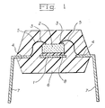
- Fig. 1 in the drawing contains a schematic cross section of the semiconductor device used to evaluate the properties of the conductive adhesive in the examples of the present invention.
- the main components of the conductive addition reaction-curing silicone rubber composition used by the present invention comprise organopolysiloxane having silicon-bonded alkenyl groups, SiH-containing organopolysiloxane, hydrosilylation reaction catalyst, and conductive filler, and this composition forms a conductive silicone rubber by curing at room temperature or with heating.
- this conductive addition reaction-curing silicone rubber composition contain ⁇ 500 ppm low-molecular-weight siloxane having a vapor pressure > 10 mmHg at 200°C. Both the wire bondability and the moisture resistance are reduced when the content of such low-molecular-weight siloxane exceeds 500 ppm.
- This low-molecular-weight siloxane may be linear or cyclic, and is exemplified by cyclic siloxane as represented by the following formula in the preceding formula, n is an integer with a value of 3 to 25 and by linear siloxane as represented by the following formula
- m is an integer with a value of 1 to 25.
- the content of this low-molecular-weight siloxane can be easily determined by extracting the low-molecular-weight siloxane from the organopolysiloxane or conductive addition reaction-curing silicone rubber composition using organic solvent and analyzing the extracted amount by gas chromato-graphy. This can also be measured by gas chromatographic analysis of the gases developed when the conductive addition reaction-curing silicone rubber composition is heated.
- the conductive addition reaction-curing silicone rubber composition of the present invention preferably consists of the following:
- the organopolysiloxane having silicon-bonded alkenyl groups, component (A), comprises organopolysiloxane which has at least two silicon-bonded alkenyl groups in each molecule and which is represented by the following average unit formula
- R2 a SiO (4 - a)/2 in the preceding formula
- R2 is a monovalent hydrocarbon group as illustrated by alkyl groups such as methyl, ethyl, propyl, and so forth, aryl groups such as phenyl, tolyl, and so forth, alkenyl groups such as vinyl, allyl, propenyl, hexenyl, and so forth; and a has a value of 1 to 3.
- organopolysiloxane can be prepared by those methods known to the individual skilled in the art, it will generally contain as a by-product approximately 2 to 7 weights low-molecular-weight siloxane having a vapor pressure > 10 mmHg at 200°C, such as octamethyltetracyclosiloxane, decamethylpentacyclosiloxane, dodecamethylhexacyclosiloxane, and so forth.
- Organopolysiloxane comprising component (A) used by the present invention can be prepared by removing this low-molecular-weight siloxane from the aforementioned organopoly-siloxane, and numerous methods are available for this removal of low-molecular-weight siloxane.
- useable methods include, inter alia, conversion of the organopolysiloxane into a thin film and stripping at 180 to 300°C in a vacuum ( ⁇ 0.5 mmHg), but also extraction of the low-molecular-weight siloxane by the addition to the organopolysiloxane of a solvent such as methanol, ethanol, propanol, butanol, or acetone.
- the organopolysiloxane comprising component (A) should have a viscosity within the range of 50 to 500,000 centistokes (cs) at 25°C, while viscosities within the range of 400 to 100,000 cs are particularly suitable.
- the organohydrogenpolysiloxane comprising component (B) is a crosslinker for component (A), and should contain at least 2 silicon-bonded hydrogen atoms in each molecule. Its molecular structure may be any of linear, branched, or cyclic.
- This organohydrogenpolysiloxane should be admixed in a quantity sufficient for this component to furnish 0.5 to 3 silicon-bonded hydrogen atoms per alkenyl group in component (A). Quantities sufficient to provide 1 to 2 silicon-bonded hydrogen atoms are preferred. This quantity generally will not exceed 2 weight% of component (A). Furthermore, in order that component (B) contain low-molecular-weight siloxane comparable with component (A), the use is preferred of a component (B) from which the low-molecular-weight siloxane by-product has been removed, for example, by stripping at 180 to 3O0°C in a vacuum > 0.5 mmHg.
- organopolysiloxane under consideration is exemplified as follows. in the preceding formulas, b , c , d , e , and g are zero or a positive integer and f is an integer with a value of at least 2.
- R1 monovalent hydrocarbon group such as methyl, ethyl, propyl, propenyl, etc, and which also contains the lower alkenyl group or silicon-bonded hydrogen atom.
- the platinum-type catalyst comprising component (D) is a catalyst for curing the conductive adhesive of the present invention, and usable in this regard are those generally known as addition-reaction catalysts for use in the hydrosilylation reaction.
- addition-reaction catalysts for use in the hydrosilylation reaction.
- examples here are platinum black, solid platinum supported on a carrier such as alumina or silica, chloroplatinic acid, alcohol-modified chloroplatinic acid, olefin/chloroplatinic acid complexes, and platinum/vinylsiloxane complexes.
- the solid catalysts should be sufficiently finely ground, or the particle size of their supports should be small enough, to give good dispersibility, and large specific surface areas are preferred.
- Chloroplatinic acid and its complexes with olefin are advantageously used dissolved in a solvent such as alcohol, ketone, ether, or hydrocarbon.
- a solvent such as alcohol, ketone, ether, or hydrocarbon.
- the quantity of addition of such catalysts should be suitably adjusted so as to afford the desired curing rate.
- those catalysts compatible with siloxane, such as chloroplatinic acid and so forth a range of 1 to 100 ppm as platinum referred to the total quantity of components (A) and (B) is preferred for obtaining a good cured product.
- microparticulate silica filler comprising component (E) is admixed in order to impart an appropriate hardness, strength, and workability to the conductive adhesive of the present invention, and it generally comprises those fillers used in addition reaction-curing silicone rubber compositions.
- Such microparticulate silica fillers are exemplified by fumed silica, precipitated silica, hydrophobicized silica, and so forth. It is added at no more than 100 parts by weight per 100 parts by weight component (A).
- the conductive filler comprising component (F) is the essential component for imparting electrical conductivity to the conductive adhesive of the present invention.
- Conductive fillers usable in the conductive adhesive of the present invention are exemplified by the micropowders of such metals as gold, silver, nickel, copper, and so forth, but also by micropowders in which a metal including gold, silver, nickel, and copper has been plated or vapor-deposited on the surface of ceramic micropowder, glass micropowder, microparticulate quartz, microparticulate organic resin, and so forth.
- usable conductive fillers comprise gold micropowder and silver micropowder, but microparticulate silver is the practical choice.
- This silver powder may take a spherical, flake, or dendritic flake form.
- Flake silver powder or dendritic flake silver powder is preferred for obtaining conductive silicone rubber with a conductivity below 1 x 10⁻³ ohm-cm.
- the mixing weight ratio of flake silver powder to dendritic flake silver powder is preferably 80/20 to 20/80.
- the particle size of the silver powder should be 1 to 10 micrometers and preferably is 1 to 5 micrometers.
- component (F) is admixed at 50 to 2,000 parts by weight and preferably 300 to 600 parts by weight per 100 parts weight component (A).
- the conductivity which is an object of the present invention is not expressed at an addition of less than 50 parts by weight.
- the workability of the conductive adhesive is degraded at an addition in excess of 2,000 parts by weight.
- the content of low-molecular-weight siloxane and the properties of the conductive adhesive were measured according to the following methods.
- the low-molecular-weight siloxane was extracted with acetone from the starting organopolysiloxane, and the amount extracted was measured by gas chromatography with flame ionization detector (FID).
- Semiconductor pellet cracking was evaluated as follows. Conductive adhesive 8 was placed between semiconductor pellet 2 and tab 1 and heated for 1 minute at 200°C. After cooling the obtained unified assembly comprising semiconductor pellet 2 and tab 1 bonded via conductive adhesive 8 , the surface of the semiconductor pellet 2 was evaluated under a microscope for pellet cracking.
- Wire bondability was evaluated as follows.
- the aluminum bonding pads 3 on the assembly afforded by the preceding evaluation of semiconductor pellet cracking were bonded to a copper inner lead frame 4 by gold wires 5 (wire bonding) to give another unified assembly.
- the gold wires 5 were bonded by ultrasonic hot-press bonding.
- the bonding points between the gold wires 5 and aluminum bonding pads 3 and between the gold wires 5 and copper inner lead frame 4 in this assembly were then inspected.
- the gold wires 5 were pulled on at the same time, and defective bonding was scored when a gold wire 5 could be lifted up. The number of defective connections is reported referred to the total number of tested connections.
- Moisture resistance was evaluated as follows. The unified assembly obtained in the aforementioned evaluation of wire bondability was sealed with epoxy resin 6 in order to manufacture a semiconductor device. This semiconductor device was then heated for the specified time in saturated steam (2 atm, 121°C). After heating, current was applied to the semiconductor device, and the leakage current across the copper inner frame 4 was measured. The semiconductor device was scored as defective in the case of an increased leakage current and pass-through defect. The number of defects is reported relative to the total number of semiconductor devices.
- Conductivity was measured as follows. A 1 mm-thick cured sheet of the conductive silicone rubber was prepared and measured using a resistivity measurement instrument (K-705RL from Kyowa Riken Yugengaisha).
- Disiloxane with the following formula and cyclic siloxane with the following formula were polymerized using potassium silanolate catalyst, and a vinyl group-containing dimethylpolysiloxane (I) was obtained by neutralization.
- This vinyl group-containing dimethylpolysiloxane (I) was stripped for 5 hours at 10 mmHg/180°C in order to remove low-molecular-weight siloxane, and vinyl group-containing dimethylpolysiloxane (II) with a viscosity of 2,000 cs was obtained.
- the quantities of low-molecular-weight siloxane contained in these dimethylpolysiloxanes (I) and (II) were determined by gas chromatography (GC-9A from Shimadzu Seisakujo Kabushiki Kaisha, FID): its content in dimethylpolysiloxane (I) was 20.5 weight% and its content in dimethylpolysiloxane (II) was 1.3 weight%, and the main component of the low-molecular-weight siloxane with vapor pressure > 10 mmHg at 200°C was the cyclic dimethylpolysiloxane decamer (D10).
- Dimethylpolysiloxane (II) was additionally subjected to molecular distillation for 8 hours at 260°C/0.01 mmHg in order to remove the low-molecular-weight siloxane.
- the content of low-molecular-weight siloxane to the decamer (D10) in the obtained vinyl group-containing dimethylpolysiloxane (III) was 0.01 weight%.
- This dimethylpolysiloxane resin (V) contained 10 ppm low-molecular-weight siloxane to the decamer (D10).
- Disiloxane with the following formula cyclic siloxane with the following formula and cyclic siloxane with the following formula were polymerized in the presence of sulfuric acid catalyst, and neutralization afforded the SiH-containing polysiloxane (VI) with the following average formula.
- This polysiloxane (VI) was stripped for 3 hours at 180°C under a 0.5 mmHg vacuum to give SiH-containing polysiloxane (VII) with a reduced content of low-molecular-weight siloxane.
- the content of low-molecular-weight siloxane to the decamer (D10) in polysiloxanes (VI) and (VII) was 17.0 weight% in (VI) and 100 ppm in (VII).
- a conductive addition reaction-curing silicone rubber composition was prepared proceeding as in Example 1 with the following modifications: vinyl-containing dimethylpolysiloxane (II) was used in place of vinyl-containing dimethylpolysiloxane (IV) in Example 1, and SiH-containing polysiloxane (VI) was used in place of the SiH-containing polysiloxane (VII) prepared in Reference Example 3.
- This composition contained 2,800 ppm low-molecular-weight siloxane. The volatile component developed upon curing this composition (200°C/10 minutes) was measured by gas chromatography at 3,560 ppm. The resistivity of the conductive silicone rubber obtained by curing this composition was 4x10 ⁇ 4 ohm-cm.
- This composition was then used as a conductive adhesive in semiconductor device production, and its semiconductor pellet cracking, wire bondability, and moisture resistance were measured as in Example 1. These results are also reported in Table 1.
- the conductive adhesive according to the present invention consists of a conductive addition reaction-curing silicone rubber composition which contains ⁇ 500 ppm low-molecular-weight siloxane with vapor pressure > 10 mmHg at 200°C. Accordingly, when used as a conductive adhesive (conductive die bonding agent) for bonding a semiconductor pellet to the tab, in contrast to conventional conductive addition reaction-curing silicone rubber compositions there is no reduction in wire bondability, no reduction in adhesiveness between sealant resin and semiconductor pellet surface or lead frame, and no reduction in the semiconductor device's moisture resistance.
- this conductive adhesive is distinguished by its ability to reduce changes in the properties of the semiconductor device and to prevent cracking and bending of the semiconductor pellet, which derive from its capacity to absorb and reduce the stresses which develop between these two components.
Landscapes
- Engineering & Computer Science (AREA)
- Computer Hardware Design (AREA)
- Microelectronics & Electronic Packaging (AREA)
- Power Engineering (AREA)
- Physics & Mathematics (AREA)
- Condensed Matter Physics & Semiconductors (AREA)
- General Physics & Mathematics (AREA)
- Chemical & Material Sciences (AREA)
- Chemical Kinetics & Catalysis (AREA)
- Organic Chemistry (AREA)
- Adhesives Or Adhesive Processes (AREA)
- Connections Effected By Soldering, Adhesion, Or Permanent Deformation (AREA)
- Compositions Of Macromolecular Compounds (AREA)
Applications Claiming Priority (2)
| Application Number | Priority Date | Filing Date | Title |
|---|---|---|---|
| JP1311013A JP2974700B2 (ja) | 1989-11-30 | 1989-11-30 | 導電性接着剤 |
| JP311013/89 | 1989-11-30 |
Publications (3)
| Publication Number | Publication Date |
|---|---|
| EP0430255A2 true EP0430255A2 (fr) | 1991-06-05 |
| EP0430255A3 EP0430255A3 (en) | 1991-09-25 |
| EP0430255B1 EP0430255B1 (fr) | 1994-09-21 |
Family
ID=18012074
Family Applications (1)
| Application Number | Title | Priority Date | Filing Date |
|---|---|---|---|
| EP90122877A Expired - Lifetime EP0430255B1 (fr) | 1989-11-30 | 1990-11-29 | Adhésif conducteur et article fabriqué avec celui-ci |
Country Status (4)
| Country | Link |
|---|---|
| US (1) | US5173765A (fr) |
| EP (1) | EP0430255B1 (fr) |
| JP (1) | JP2974700B2 (fr) |
| DE (1) | DE69012749T2 (fr) |
Cited By (9)
| Publication number | Priority date | Publication date | Assignee | Title |
|---|---|---|---|---|
| EP0757080A2 (fr) * | 1995-08-04 | 1997-02-05 | Dow Corning Toray Silicone Company Ltd. | Compositions durcissables d'organosiloxane et dispositifs semi-conducteur |
| EP0779653A2 (fr) * | 1995-12-11 | 1997-06-18 | Dow Corning Corporation | Adhésif conductif en silicone, sensible de la pression, pour la technique à pastile renversée |
| EP0824270A2 (fr) * | 1996-08-06 | 1998-02-18 | Hitachi Chemical Co., Ltd. | Procédé pour le montage d'une pluralité de pièces électroniques sur un panneau de circuit |
| EP0943438A1 (fr) * | 1998-03-10 | 1999-09-22 | Nec Corporation | Tête à jet d'encre pour imprimante sans impact |
| EP0949675A3 (fr) * | 1998-03-26 | 2000-04-19 | Nec Corporation | Capteur d'images à l'état solide thermorésistant et procédé pour sa fabrication |
| EP1039480A1 (fr) * | 1999-03-25 | 2000-09-27 | Shin-Etsu Chemical Co., Ltd. | Composition de caoutchouc de silicone conductrice et connecteur à basse résistance |
| EP1278211A1 (fr) * | 2001-07-17 | 2003-01-22 | Shin-Etsu Chemical Co., Ltd. | Composition conductrice |
| WO2003046098A1 (fr) * | 2001-11-28 | 2003-06-05 | Dow Corning Toray Silicone Co., Ltd. | Film adhesif anisotropiquement electroconducteur, procede de production associe et dispositifs semiconducteurs |
| CN108102578A (zh) * | 2017-12-21 | 2018-06-01 | 上海市合成树脂研究所有限公司 | 一种导电胶的制备方法 |
Families Citing this family (28)
| Publication number | Priority date | Publication date | Assignee | Title |
|---|---|---|---|---|
| KR970008355B1 (ko) * | 1992-09-29 | 1997-05-23 | 가부시키가이샤 도시바 | 수지밀봉형 반도체장치 |
| US5441726A (en) * | 1993-04-28 | 1995-08-15 | Sunsmart, Inc. | Topical ultra-violet radiation protectants |
| US5391432A (en) * | 1993-04-28 | 1995-02-21 | Mitchnick; Mark | Antistatic fibers |
| AU6627394A (en) * | 1993-04-28 | 1994-11-21 | Mark Mitchnick | Conductive polymers |
| US5384284A (en) * | 1993-10-01 | 1995-01-24 | Micron Semiconductor, Inc. | Method to form a low resistant bond pad interconnect |
| DE69407137T2 (de) * | 1993-10-06 | 1998-04-09 | Dow Corning Toray Silicone | Mit Silber gefüllte, elektrisch leitfähige Organosiloxan-Zusammensetzungen |
| JP3950490B2 (ja) * | 1995-08-04 | 2007-08-01 | 東レ・ダウコーニング株式会社 | 導電性シリコーンゴム組成物および半導体装置 |
| JPH09286971A (ja) * | 1996-04-19 | 1997-11-04 | Toray Dow Corning Silicone Co Ltd | シリコーン系ダイボンディング剤、半導体装置の製造方法および半導体装置 |
| JP3950493B2 (ja) * | 1996-04-26 | 2007-08-01 | 東レ・ダウコーニング株式会社 | 導電性シリコーンゴム組成物、半導体装置の製造方法およびその半導体装置 |
| DE69715504T2 (de) * | 1996-04-26 | 2003-06-05 | Dow Corning Toray Silicone | Elektrisch leitfähige Silikonkautschukzusammensetzung und ihre Anwendung zur Herstellung von Halbleiteranordnungen |
| JP3417247B2 (ja) * | 1996-05-28 | 2003-06-16 | 株式会社デンソー | 樹脂封止型電子装置の製造方法 |
| JP3436464B2 (ja) * | 1996-10-31 | 2003-08-11 | 東レ・ダウコーニング・シリコーン株式会社 | 付加反応硬化型導電性シリコーン組成物および導電性シリコーン硬化物の製造方法 |
| US6916433B2 (en) * | 2000-02-29 | 2005-07-12 | Matsushita Electric Industrial Co., Ltd. | Conductive adhesive, apparatus for mounting electronic component, and method for mounting the same |
| US6361716B1 (en) * | 2000-07-20 | 2002-03-26 | Dow Corning Corporation | Silicone composition and electrically conductive silicone adhesive formed therefrom |
| US6784555B2 (en) * | 2001-09-17 | 2004-08-31 | Dow Corning Corporation | Die attach adhesives for semiconductor applications utilizing a polymeric base material with inorganic insulator particles of various sizes |
| JP3999994B2 (ja) * | 2002-04-03 | 2007-10-31 | 東レ・ダウコーニング株式会社 | 導電性シリコーンゴム組成物 |
| JP4597508B2 (ja) * | 2003-12-10 | 2010-12-15 | モメンティブ・パフォーマンス・マテリアルズ・ジャパン合同会社 | 半導体ペレットと半導体ペレット取付部材とを接合するためのシリコーン接着剤 |
| JP2006073950A (ja) * | 2004-09-06 | 2006-03-16 | Kansai Electric Power Co Inc:The | 高耐熱半導体装置 |
| US20060094809A1 (en) * | 2004-11-02 | 2006-05-04 | Simone Davide L | Electrically and thermally conductive silicone adhesive compositions |
| JP2007035965A (ja) * | 2005-07-27 | 2007-02-08 | Oki Electric Ind Co Ltd | 半導体装置およびその製造方法、ならびにそれに使用される接着材料およびその製造方法 |
| JP5060074B2 (ja) * | 2006-05-11 | 2012-10-31 | 東レ・ダウコーニング株式会社 | 接着促進剤、硬化性オルガノポリシロキサン組成物、および半導体装置 |
| US20070284758A1 (en) * | 2006-05-22 | 2007-12-13 | General Electric Company | Electronics package and associated method |
| CN103237863B (zh) * | 2010-12-20 | 2015-07-08 | 施敏打硬株式会社 | 导电性粘接剂 |
| JP5854522B2 (ja) * | 2013-07-16 | 2016-02-09 | 国立研究開発法人産業技術総合研究所 | 接着材組成物 |
| JP6348434B2 (ja) * | 2014-03-28 | 2018-06-27 | 信越化学工業株式会社 | シリコーン粘着剤組成物、その製造法及び粘着フィルム |
| KR20150112851A (ko) * | 2014-03-28 | 2015-10-07 | 신에쓰 가가꾸 고교 가부시끼가이샤 | 실리콘 점착제 조성물, 그의 제조 방법 및 점착 필름 |
| JP6870258B2 (ja) | 2016-09-23 | 2021-05-12 | 日亜化学工業株式会社 | 導電性接着剤および導電性材料 |
| CN111138836B (zh) * | 2020-01-02 | 2022-03-08 | 深圳先进技术研究院 | 一种柔性电磁屏蔽复合材料及其制备方法 |
Citations (4)
| Publication number | Priority date | Publication date | Assignee | Title |
|---|---|---|---|---|
| US4051454A (en) * | 1973-02-16 | 1977-09-27 | Wacker-Chemie Gmbh | Adhesive compositions and flexible heating device fabricated therewith |
| US4721994A (en) * | 1985-06-25 | 1988-01-26 | Toray Silicone Co., Ltd. | Lead frame for semiconductor devices |
| EP0269567A2 (fr) * | 1986-11-14 | 1988-06-01 | Ciba-Geigy Ag | Composition potentiellement adhésive électriquement conductrice |
| EP0273003A1 (fr) * | 1986-10-20 | 1988-06-29 | Ciba-Geigy Ag | Composition potentiellement adhésive électriquement conductrice |
Family Cites Families (4)
| Publication number | Priority date | Publication date | Assignee | Title |
|---|---|---|---|---|
| JPS5886732A (ja) * | 1981-11-18 | 1983-05-24 | Clarion Co Ltd | 半導体素子 |
| JPS62240361A (ja) * | 1986-04-11 | 1987-10-21 | Toray Silicone Co Ltd | 硬化性オルガノポリシロキサン組成物 |
| JP2585006B2 (ja) * | 1987-07-22 | 1997-02-26 | 東レ・ダウコーニング・シリコーン株式会社 | 樹脂封止型半導体装置およびその製造方法 |
| JP2882823B2 (ja) | 1989-11-15 | 1999-04-12 | 東レ・ダウコーニング・シリコーン株式会社 | 接着剤 |
-
1989
- 1989-11-30 JP JP1311013A patent/JP2974700B2/ja not_active Expired - Lifetime
-
1990
- 1990-11-29 EP EP90122877A patent/EP0430255B1/fr not_active Expired - Lifetime
- 1990-11-29 US US07/619,842 patent/US5173765A/en not_active Expired - Lifetime
- 1990-11-29 DE DE69012749T patent/DE69012749T2/de not_active Expired - Lifetime
Patent Citations (4)
| Publication number | Priority date | Publication date | Assignee | Title |
|---|---|---|---|---|
| US4051454A (en) * | 1973-02-16 | 1977-09-27 | Wacker-Chemie Gmbh | Adhesive compositions and flexible heating device fabricated therewith |
| US4721994A (en) * | 1985-06-25 | 1988-01-26 | Toray Silicone Co., Ltd. | Lead frame for semiconductor devices |
| EP0273003A1 (fr) * | 1986-10-20 | 1988-06-29 | Ciba-Geigy Ag | Composition potentiellement adhésive électriquement conductrice |
| EP0269567A2 (fr) * | 1986-11-14 | 1988-06-01 | Ciba-Geigy Ag | Composition potentiellement adhésive électriquement conductrice |
Non-Patent Citations (1)
| Title |
|---|
| Proceedings of the 39th Electronic Components Conference,Houston,Tx,May 22-24,1989;New York,US p.83-87; M.A.LUTZ et al.:"Flexible silicone adhesive with high electrical conductivity" * |
Cited By (22)
| Publication number | Priority date | Publication date | Assignee | Title |
|---|---|---|---|---|
| EP0757080A2 (fr) * | 1995-08-04 | 1997-02-05 | Dow Corning Toray Silicone Company Ltd. | Compositions durcissables d'organosiloxane et dispositifs semi-conducteur |
| EP0757080A3 (fr) * | 1995-08-04 | 1997-07-02 | Dow Corning Toray Silicone | Compositions durcissables d'organosiloxane et dispositifs semi-conducteur |
| EP1231242A1 (fr) * | 1995-08-04 | 2002-08-14 | Dow Corning Toray Silicone Company Ltd. | Compositions durcissables d'organosiloxane et dispositifs semi-conducteur |
| EP0779653A2 (fr) * | 1995-12-11 | 1997-06-18 | Dow Corning Corporation | Adhésif conductif en silicone, sensible de la pression, pour la technique à pastile renversée |
| EP0779653A3 (fr) * | 1995-12-11 | 1999-01-20 | Dow Corning Corporation | Adhésif conductif en silicone, sensible de la pression, pour la technique à pastile renversée |
| US6158115A (en) * | 1996-08-06 | 2000-12-12 | Hitachi Chemical Company, Ltd. | Method of mounting a plurality of electronic parts on a circuit board |
| US6479757B1 (en) | 1996-08-06 | 2002-11-12 | Hitachi Chemical Company, Ltd. | Method of mounting a plurality of electronic parts on a circuit board |
| US6841022B2 (en) | 1996-08-06 | 2005-01-11 | Hitachi Chemical Company, Ltd. | Adhesive-coated electronic parts on a connection sheet |
| EP0824270A2 (fr) * | 1996-08-06 | 1998-02-18 | Hitachi Chemical Co., Ltd. | Procédé pour le montage d'une pluralité de pièces électroniques sur un panneau de circuit |
| EP0824270A3 (fr) * | 1996-08-06 | 1999-06-09 | Hitachi Chemical Co., Ltd. | Procédé pour le montage d'une pluralité de pièces électroniques sur un panneau de circuit |
| US6345887B1 (en) | 1998-03-10 | 2002-02-12 | Nec Corporation | Ink jet head for non-impact printer |
| EP0943438A1 (fr) * | 1998-03-10 | 1999-09-22 | Nec Corporation | Tête à jet d'encre pour imprimante sans impact |
| US6144107A (en) * | 1998-03-26 | 2000-11-07 | Nec Corporation | Solid state pickup device excellent in heat-resistance and method of manufacturing the device |
| EP0949675A3 (fr) * | 1998-03-26 | 2000-04-19 | Nec Corporation | Capteur d'images à l'état solide thermorésistant et procédé pour sa fabrication |
| US6309563B1 (en) | 1999-03-25 | 2001-10-30 | Shin-Etsu Chemical Co., Ltd. | Conductive silicone rubber composition and low-resistance connector |
| EP1039480A1 (fr) * | 1999-03-25 | 2000-09-27 | Shin-Etsu Chemical Co., Ltd. | Composition de caoutchouc de silicone conductrice et connecteur à basse résistance |
| EP1278211A1 (fr) * | 2001-07-17 | 2003-01-22 | Shin-Etsu Chemical Co., Ltd. | Composition conductrice |
| US6835331B2 (en) | 2001-07-17 | 2004-12-28 | Shin-Etsu Chemical Co., Ltd. | Conductive composition |
| KR100871787B1 (ko) * | 2001-07-17 | 2008-12-05 | 신에쓰 가가꾸 고교 가부시끼가이샤 | 도전성 조성물 |
| WO2003046098A1 (fr) * | 2001-11-28 | 2003-06-05 | Dow Corning Toray Silicone Co., Ltd. | Film adhesif anisotropiquement electroconducteur, procede de production associe et dispositifs semiconducteurs |
| KR100913686B1 (ko) * | 2001-11-28 | 2009-08-24 | 다우 코닝 도레이 캄파니 리미티드 | 이방성 전기 전도성 접착 필름, 이의 제조방법 및 이를 포함하는 반도체 장치 |
| CN108102578A (zh) * | 2017-12-21 | 2018-06-01 | 上海市合成树脂研究所有限公司 | 一种导电胶的制备方法 |
Also Published As
| Publication number | Publication date |
|---|---|
| DE69012749D1 (de) | 1994-10-27 |
| EP0430255A3 (en) | 1991-09-25 |
| EP0430255B1 (fr) | 1994-09-21 |
| DE69012749T2 (de) | 1995-03-02 |
| JP2974700B2 (ja) | 1999-11-10 |
| US5173765A (en) | 1992-12-22 |
| JPH03170581A (ja) | 1991-07-24 |
Similar Documents
| Publication | Publication Date | Title |
|---|---|---|
| EP0430255B1 (fr) | Adhésif conducteur et article fabriqué avec celui-ci | |
| EP0432502B1 (fr) | Colle pour composant semi-conducteur et objets fabriqués au moyen de cette colle | |
| EP0908499B1 (fr) | Composition réticulable de silicone et composants électroniques | |
| KR100591875B1 (ko) | 실리콘 조성물, 이의 제조방법 및 실리콘 탄성중합체 | |
| EP2528974B1 (fr) | Composition de caoutchouc de silicone thermiquement conducteur | |
| JP3436464B2 (ja) | 付加反応硬化型導電性シリコーン組成物および導電性シリコーン硬化物の製造方法 | |
| KR101280277B1 (ko) | 절연성 액상 다이 결합제 및 반도체 디바이스 | |
| KR100655626B1 (ko) | 실리콘계 접착성 시트 및 이의 제조방법 | |
| WO2006077667A1 (fr) | Composition de silicone pour encapsuler un element luminescent et dispositif luminescent | |
| CN1528000A (zh) | 导电性有机硅及其制造方法 | |
| JPH10212413A (ja) | 電気・電子部品封止・充填用シリコーンゲル組成物およびシリコーンゲル | |
| KR20010049725A (ko) | 접착제 및 반도체 장치 | |
| JP3207929B2 (ja) | 半導体素子被覆剤および半導体装置 | |
| EP1067163B1 (fr) | Adhésif et dispositifs semi-conducteurs | |
| EP3587498A1 (fr) | Composition de silicone durcissable et dispositif à semi-conducteur | |
| JP3519779B2 (ja) | 接着剤および半導体装置 | |
| JPH1025417A (ja) | 硬化性液状組成物、その硬化物、および電子部品 | |
| JP3915885B2 (ja) | 半導体部品用シリコーン接着剤 | |
| JPH09310024A (ja) | 硬化性オルガノポリシロキサン組成物および半導体装置 | |
| US20110180938A1 (en) | Electronic device and method of manufacturing the same | |
| CN116855226A (zh) | 一种用于裸芯片的双组份导热凝胶及其制备方法 | |
| KR20020081640A (ko) | 실리콘 조성물 및 이로부터 제조된 전기 전도성 실리콘접착제 | |
| TW202233758A (zh) | 聚矽氧組合物 | |
| JP2014229817A (ja) | 半導体装置 |
Legal Events
| Date | Code | Title | Description |
|---|---|---|---|
| PUAI | Public reference made under article 153(3) epc to a published international application that has entered the european phase |
Free format text: ORIGINAL CODE: 0009012 |
|
| 17P | Request for examination filed |
Effective date: 19910102 |
|
| AK | Designated contracting states |
Kind code of ref document: A2 Designated state(s): DE FR GB |
|
| PUAL | Search report despatched |
Free format text: ORIGINAL CODE: 0009013 |
|
| AK | Designated contracting states |
Kind code of ref document: A3 Designated state(s): DE FR GB |
|
| 17Q | First examination report despatched |
Effective date: 19931221 |
|
| GRAA | (expected) grant |
Free format text: ORIGINAL CODE: 0009210 |
|
| AK | Designated contracting states |
Kind code of ref document: B1 Designated state(s): DE FR GB |
|
| REF | Corresponds to: |
Ref document number: 69012749 Country of ref document: DE Date of ref document: 19941027 |
|
| ET | Fr: translation filed | ||
| PLBE | No opposition filed within time limit |
Free format text: ORIGINAL CODE: 0009261 |
|
| STAA | Information on the status of an ep patent application or granted ep patent |
Free format text: STATUS: NO OPPOSITION FILED WITHIN TIME LIMIT |
|
| 26N | No opposition filed | ||
| REG | Reference to a national code |
Ref country code: GB Ref legal event code: IF02 |
|
| PGFP | Annual fee paid to national office [announced via postgrant information from national office to epo] |
Ref country code: GB Payment date: 20031006 Year of fee payment: 14 |
|
| PG25 | Lapsed in a contracting state [announced via postgrant information from national office to epo] |
Ref country code: GB Free format text: LAPSE BECAUSE OF NON-PAYMENT OF DUE FEES Effective date: 20041129 |
|
| GBPC | Gb: european patent ceased through non-payment of renewal fee |
Effective date: 20041129 |
|
| PGFP | Annual fee paid to national office [announced via postgrant information from national office to epo] |
Ref country code: DE Payment date: 20091126 Year of fee payment: 20 |
|
| PGFP | Annual fee paid to national office [announced via postgrant information from national office to epo] |
Ref country code: FR Payment date: 20091123 Year of fee payment: 20 |
|
| PG25 | Lapsed in a contracting state [announced via postgrant information from national office to epo] |
Ref country code: DE Free format text: LAPSE BECAUSE OF EXPIRATION OF PROTECTION Effective date: 20101129 |