EP0419823B1 - Digital time base generator with adjustable delay between two outputs - Google Patents
Digital time base generator with adjustable delay between two outputs Download PDFInfo
- Publication number
- EP0419823B1 EP0419823B1 EP90115488A EP90115488A EP0419823B1 EP 0419823 B1 EP0419823 B1 EP 0419823B1 EP 90115488 A EP90115488 A EP 90115488A EP 90115488 A EP90115488 A EP 90115488A EP 0419823 B1 EP0419823 B1 EP 0419823B1
- Authority
- EP
- European Patent Office
- Prior art keywords
- frequency
- reference signal
- time
- output
- integer
- Prior art date
- Legal status (The legal status is an assumption and is not a legal conclusion. Google has not performed a legal analysis and makes no representation as to the accuracy of the status listed.)
- Expired - Lifetime
Links
- 230000009977 dual effect Effects 0.000 claims description 11
- 239000013078 crystal Substances 0.000 claims description 6
- 238000000034 method Methods 0.000 claims description 6
- 238000000926 separation method Methods 0.000 claims description 3
- 238000004519 manufacturing process Methods 0.000 claims description 2
- 230000005540 biological transmission Effects 0.000 description 29
- 238000005259 measurement Methods 0.000 description 19
- 229920000729 poly(L-lysine) polymer Polymers 0.000 description 5
- 230000000630 rising effect Effects 0.000 description 5
- 238000010586 diagram Methods 0.000 description 4
- 230000000694 effects Effects 0.000 description 3
- 230000010355 oscillation Effects 0.000 description 2
- 230000001154 acute effect Effects 0.000 description 1
- 230000003247 decreasing effect Effects 0.000 description 1
- 230000001934 delay Effects 0.000 description 1
- 230000003111 delayed effect Effects 0.000 description 1
- 230000001419 dependent effect Effects 0.000 description 1
Images

Classifications
-
- H—ELECTRICITY
- H03—ELECTRONIC CIRCUITRY
- H03L—AUTOMATIC CONTROL, STARTING, SYNCHRONISATION OR STABILISATION OF GENERATORS OF ELECTRONIC OSCILLATIONS OR PULSES
- H03L7/00—Automatic control of frequency or phase; Synchronisation
- H03L7/06—Automatic control of frequency or phase; Synchronisation using a reference signal applied to a frequency- or phase-locked loop
- H03L7/16—Indirect frequency synthesis, i.e. generating a desired one of a number of predetermined frequencies using a frequency- or phase-locked loop
- H03L7/22—Indirect frequency synthesis, i.e. generating a desired one of a number of predetermined frequencies using a frequency- or phase-locked loop using more than one loop
-
- H—ELECTRICITY
- H03—ELECTRONIC CIRCUITRY
- H03K—PULSE TECHNIQUE
- H03K5/00—Manipulating of pulses not covered by one of the other main groups of this subclass
- H03K5/15—Arrangements in which pulses are delivered at different times at several outputs, i.e. pulse distributors
- H03K5/15006—Arrangements in which pulses are delivered at different times at several outputs, i.e. pulse distributors with two programmable outputs
-
- H—ELECTRICITY
- H03—ELECTRONIC CIRCUITRY
- H03K—PULSE TECHNIQUE
- H03K5/00—Manipulating of pulses not covered by one of the other main groups of this subclass
- H03K5/15—Arrangements in which pulses are delivered at different times at several outputs, i.e. pulse distributors
-
- H—ELECTRICITY
- H03—ELECTRONIC CIRCUITRY
- H03L—AUTOMATIC CONTROL, STARTING, SYNCHRONISATION OR STABILISATION OF GENERATORS OF ELECTRONIC OSCILLATIONS OR PULSES
- H03L7/00—Automatic control of frequency or phase; Synchronisation
- H03L7/06—Automatic control of frequency or phase; Synchronisation using a reference signal applied to a frequency- or phase-locked loop
- H03L7/16—Indirect frequency synthesis, i.e. generating a desired one of a number of predetermined frequencies using a frequency- or phase-locked loop
- H03L7/22—Indirect frequency synthesis, i.e. generating a desired one of a number of predetermined frequencies using a frequency- or phase-locked loop using more than one loop
- H03L7/23—Indirect frequency synthesis, i.e. generating a desired one of a number of predetermined frequencies using a frequency- or phase-locked loop using more than one loop with pulse counters or frequency dividers
Definitions
- This invention relates in general to time base generator circuits, and particularly to circuits which produce digital timing signals used for calibrating time measurement systems.
- Digital time base generator circuits are circuits which produce a signal having pulse edges separated by a known relationship in time, hereinafter called a time reference signal.
- Time base generator circuits are also known as timing signal generators or time standards.
- a time base generator circuit should produce a signal having a period which is the same length or smaller than the minimum time period to be measured. Circuits which produce a signal in the range of one Hz, for example, are commonly used in watches and clocks, where one second is the minimum time period to be measured.
- Time measurement circuits produce an output that is proportional to the amount of time that passes between two events, usually between two pulses on a signal line. Calibration of these time measurement systems involves inputting a signal with a known time delay and comparing the measurement systems output with the known time delay.
- the input signal comprises a start signal and stop signal wherein an edge of the start signal triggers the time measurement system to begin measuring time and an edge of the stop signal triggers the time measurement system to stop.
- the separation, or delay, between the edges of the start and stop signal must be extremely accurate in order to calibrate the time measurement circuits. Because switching speed and gate delay time of some circuits is in the order of picoseconds (ps), it is necessary for the time measurement system to be precise in the range of just a few picoseconds.
- circuits which produced a timing signal, or a pair of timing signals to be used as the start and stop signal described above comprised an oscillator which generated a reference signal which was then split between a first and a second transmission line.
- the first transmission line was coupled directly to the time measurement system and provided the start signal.
- the second transmission line comprised a mechanical delay line of a known time delay ⁇ t.
- a signal traveling through the second transmission line therefore, took longer to reach the end of the second transmission line than did the signal traveling through the first transmission line.
- the signals on the first and second transmission lines would be identical except out of phase by a known time delay ⁇ t which was determined by the length of the mechanical delay time.
- the signal on the first transmission line could be used as a start signal and the signal on the second transmission line could be used as a stop signal.
- Circuits using mechanical delay lines are quite bulky since even a short delay requires several feet of transmission line. Such circuits are not compatible with portable equipment, and cannot be built into a piece of equipment without increasing the size and cost of the equipment. Thus, time base generators were usually external to a piece of equipment, such as a tester, and were used only occasionally to calibrate the equipment. Time base circuits which were small enough to be built into equipment lacked the precision for many applications.
- the time base generator circuit described above resulted in standing waves on the first and second transmission lines caused by reflected energy which occurs at the termination of the transmission lines.
- the amplitude of the standing wave was a function of the frequency of oscillation on the transmission line and the characteristics of the transmission line termination.
- the standing wave interfered constructively or destructively with the signal on the transmission lines depending on the frequency of the standing wave and the length of the transmission lines. These effects became more pronounced as higher frequencies were transmitted on the transmission lines.
- the output received from the first and second transmission lines was dependent on the reference frequency and the length of the transmission lines.
- a time reference circuit must be adjustable over some range of time periods so that various time reference signals can be applied to the time measurement system during calibration.
- the oscillation frequency could be varied to change the period of the reference signal as well as the time delay between start and stop edges.
- the standing waves were generated on the first and second transmission lines even when the transmission lines were properly terminated, and resulted in noise on the transmission lines which reduced the integrity of the time base signal. Because the first and second transmission lines were different lengths, the standing wave noise effected the start and stop signals differently.
- the noise modified the time reference signal and appeared to the time measurement system as an increase or decrease in time delay of the time reference signal.
- the time reference circuit would itself have to be calibrated very carefully at each oscillator frequency before being used to calibrate a time measurement system. Since the amplitude of the standing wave increased at higher frequencies, the noise problem was particularly acute when time reference signals less than a few nanoseconds were needed.
- variable mechanical delay lines are merely transmission lines wherein the length of the transmission line can be changed by manually expanding or contracting the delay line.
- the length of the second transmission line can be increased or decreased to change the relative position of the start and stop edges produced by the time reference circuit.
- the present invention provides a circuit for producing a first and second reference signal as claimed in claim 1 and a corresponding method.
- the present invention provides a time reference circuit which can provide various time references without changing reference frequency on the signal line.
- a time reference circuit can be provided without a mechanical delay line.
- a further advantage is that the circuit can be compact and easily incorporated into a piece of equipment. Furthermore, precision in the time reference circuit can be improved by the invention and the circuit can be easily programmable.
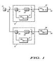
- FIG. 1 illustrates a block diagram of a time reference circuit of the present invention
- FIG. 2 illustrates a timing signal diagram of timing signals generated at various and outputs shown in Fig. 1.
- FIG. 1 illustrates a block diagram of a time reference circuit of the present invention.
- Oscillator 11 provides a reference frequency whose operation frequency f 0 is chosen to determine the precision of the final reference signal, as will be seen.
- Oscillator 11 usually comprises a crystal oscillator and in a preferred embodiment operates at 7,570,252 Hz. The accuracy of crystal oscillator 11 will eventually determine the accuracy of the output timing signal, so it is desirable to choose a crystal oscillator having an accuracy of at least 1 part/million (ppm).
- Phase locked loop 12 comprises phase detector 14, voltage control oscillator (VCO) 16, and frequency divider 17 coupled in a negative feedback loop between the output of VCO 16 and phase detector 14.
- Frequency divider 17 serves to divide an input frequency on node 18 by an integer amount N and feedback the divided frequency to phase detector 14.
- Phase detector 14 outputs a voltage to VCO 16 which is a function of a phase or frequency mismatch between reference frequency f 0 and the output of frequency divider 17.
- the voltage output of phase detector 14 causes VCO 16 to increase or decrease its output frequency until the frequencies which are input to phase detector 14 are matched. Because frequency divider 17 is in a negative feedback loop, the frequency f 0 at node 30 is multiplied by an integer multiple N which is determined by frequency divider 17.
- frequency divider 17 may be a dual modulus frequency divider which can be made to divide the frequency by N-1 for one cycle. The use of this optional function will be described hereinafter.
- Frequency divider 17 is a commercially available circuit which is also referred to as a two-modulus prescaler or a dual modulus counter. One such device is part number MC12022 sold by Motorola, Inc.
- a frequency f 1 (N) (f 0 ) is thus generated at node 18 which is then coupled to frequency divider 19.
- frequency divider 19 reduces the frequency by the same factor N as frequency divider 17.
- the output frequency at output 33 is the same as the reference frequency f 0 at node 30.
- Phase locked loop 22 comprises phase detector 24, VCO 26, and frequency divider 27. Operation of phase locked loop 22 is analogous to that of phase locked loop f 0 except that frequency divider 27 divides the frequency on node 28 by an integer M instead of N. Alternatively, frequency divider 27 can divide the frequency by M+1. Frequency f 2 on node 28 is thus an integer multiple M of the frequency f 0 on node 30. Frequency f 2 generated by phase locked loop 22 is coupled to dual modulus frequency divider 29 which divides the frequency by M, or alternatively M+1. In normal operation, frequency divider 29 divides the frequency f 2 on node 28 by the same integer factor as frequency divider 27, so that output frequency on node 34 is the same as the reference frequency f 0 on node 30.
- Output 33 is typically coupled to a start input of an external time measurement unit and node 34 is coupled to the stop input of the time measurement unit, although it should be understood that start and stop signals are interchangeable as it is the difference between the start and stop pulse edges that is used to calibrate the time measurement unit. It should be noted that both outputs 33 and 34 operate at the same frequency thus, even if standing waves are generated in the circuit, the effect of the standing waves will be the same on both start and stop signals, and thus will not be seen by the time measurement system as a change in reference time.
- Waveforms 30, 18, 28, 33, and 34 represent the frequencies and relative edge positioning of signals at the nodes and outputs shown in FIG. 1 bearing the same designation.
- Node 30 is the output of oscillator 11 and has a frequency of 1 cycle per time period.
- the output of oscillator 11 is 7,570,252 Hz, f 1 will be 976,562,508 Hz and f 2 will be 968,992,256 Hz.
- Outputs 33 and 34 illustrate first and second output signals after being divided by dual modulus frequency dividers 19 and 29 respectively.
- frequency divider 19 divides the frequency at node 18 so that output frequency at output 33 is the same as oscillator frequency f 0 at node 30.
- frequency divider 19 may be of a type that instead of dividing by N-1, divides by some other frequency N-X.
- Frequency divider 17 in PLL 12 and frequency divider 27 in PLL 22 may also be dual modulus prescalers, that is to say each of the frequency dividers 17 and 27 may have a first and second operating mode.
- the second mode of each of the prescalers can be used to shift the time separation ⁇ t between start and stop pulses at outputs 33 and 34 in a similar manner to that described in reference to frequency dividers 19 and 29. Since frequency divider 17 is coupled in the negative feedback loop, shifting to the second mode of operation results in a shift which is equal in magnitude but opposite in direction of the time shift caused by operating frequency divider 19 in the second mode as described hereinbefore. Likewise, operating frequency divider 27 in the second mode results in an equal but opposite shift to that caused by operating frequency divider 29 in the second mode.
- frequency dividers 17 and 27 are coupled in feedback loops of PLLs 12 and 22 respectively, it will take a finite amount of time for the PLLs to stabilize after the feedback loop is perturbed. This finite amount of time may be so long that it may be more advantageous to leave frequency dividers 17 and 22 in the first mode of operation, and use only frequency dividers 19 and 29 to produce time shift ⁇ t.
- the time base generator circuit provided offers a stable and adjustable time reference source which is easily made as accurate as one part per million using a conventional crystal oscillator.
Landscapes
- Physics & Mathematics (AREA)
- Nonlinear Science (AREA)
- Stabilization Of Oscillater, Synchronisation, Frequency Synthesizers (AREA)
- Electric Clocks (AREA)
- Manipulation Of Pulses (AREA)
- Synchronisation In Digital Transmission Systems (AREA)
- Measurement Of Unknown Time Intervals (AREA)
Applications Claiming Priority (2)
| Application Number | Priority Date | Filing Date | Title |
|---|---|---|---|
| US07/403,271 US4943787A (en) | 1989-09-05 | 1989-09-05 | Digital time base generator with adjustable delay between two outputs |
| US403271 | 1995-03-13 |
Publications (2)
| Publication Number | Publication Date |
|---|---|
| EP0419823A1 EP0419823A1 (en) | 1991-04-03 |
| EP0419823B1 true EP0419823B1 (en) | 1996-06-19 |
Family
ID=23595173
Family Applications (1)
| Application Number | Title | Priority Date | Filing Date |
|---|---|---|---|
| EP90115488A Expired - Lifetime EP0419823B1 (en) | 1989-09-05 | 1990-08-13 | Digital time base generator with adjustable delay between two outputs |
Country Status (7)
| Country | Link |
|---|---|
| US (1) | US4943787A (ko) |
| EP (1) | EP0419823B1 (ko) |
| JP (1) | JP2730280B2 (ko) |
| KR (1) | KR0162640B1 (ko) |
| DE (1) | DE69027493T2 (ko) |
| MY (1) | MY105977A (ko) |
| TW (1) | TW223716B (ko) |
Families Citing this family (28)
| Publication number | Priority date | Publication date | Assignee | Title |
|---|---|---|---|---|
| US5077686A (en) * | 1990-01-31 | 1991-12-31 | Stardent Computer | Clock generator for a computer system |
| GB9117635D0 (en) * | 1991-08-15 | 1991-10-02 | British Telecomm | Phase shifter |
| US5329250A (en) * | 1992-02-25 | 1994-07-12 | Sanyo Electric Co., Ltd. | Double phase locked loop circuit |
| JP2945545B2 (ja) * | 1992-04-02 | 1999-09-06 | 三菱電機株式会社 | Pll回路装置および位相差検出回路装置 |
| US5336939A (en) * | 1992-05-08 | 1994-08-09 | Cyrix Corporation | Stable internal clock generation for an integrated circuit |
| US5317284A (en) * | 1993-02-08 | 1994-05-31 | Hughes Aircraft Company | Wide band, low noise, fine step tuning, phase locked loop frequency synthesizer |
| US5317285A (en) * | 1993-02-26 | 1994-05-31 | Motorola, Inc. | Frequency synthesizer employing a continuously adaptive phase detector and method |
| US5391996A (en) * | 1993-11-19 | 1995-02-21 | General Instrument Corporation Of Delaware | Techniques for generating two high frequency signals with a constant phase difference over a wide frequency band |
| US6020733A (en) * | 1994-12-22 | 2000-02-01 | Anritsu Company | Two port handheld vector network analyzer with frequency monitor mode |
| US5642039A (en) * | 1994-12-22 | 1997-06-24 | Wiltron Company | Handheld vector network analyzer |
| US5796682A (en) * | 1995-10-30 | 1998-08-18 | Motorola, Inc. | Method for measuring time and structure therefor |
| US6049241A (en) * | 1997-02-28 | 2000-04-11 | Texas Instruments Incorporated | Clock skew circuit |
| US5977779A (en) * | 1997-10-24 | 1999-11-02 | Anritsu Company | Handheld vecor network analyzer (VNA) operating at a high frequency by mixing LO and RF signals having offset odd harmonics |
| US6356129B1 (en) * | 1999-10-12 | 2002-03-12 | Teradyne, Inc. | Low jitter phase-locked loop with duty-cycle control |
| US6807225B1 (en) * | 2000-05-31 | 2004-10-19 | Conexant Systems, Inc. | Circuit and method for self trimming frequency acquisition |
| KR100374023B1 (ko) * | 2000-08-24 | 2003-02-26 | 온재륜 | 신발창 성형프레스 자동화 장치 |
| EP1209809A1 (en) * | 2000-11-24 | 2002-05-29 | STMicroelectronics S.r.l. | Device and method for generating synchronous numeric signals |
| US6492926B2 (en) | 2000-11-24 | 2002-12-10 | Stmicroelectronics S.R.L. | Noise compensation device and method in a discrete time control system |
| US6791382B1 (en) * | 2002-04-08 | 2004-09-14 | Etron Technology, Inc. | Noise reduction method and system for a multiple clock, mixed signal integrated circuit |
| FR2848038B1 (fr) * | 2002-11-29 | 2005-12-02 | Thales Sa | Dispositif et procede de synthese de frequence a grande purete spectrale |
| US7256633B1 (en) | 2003-05-01 | 2007-08-14 | Ample Communications, Inc. | Systems for implementing high speed and high integration chips |
| US7586344B1 (en) * | 2007-10-16 | 2009-09-08 | Lattice Semiconductor Corporation | Dynamic delay or advance adjustment of oscillating signal phase |
| EP2207263B1 (en) * | 2009-01-08 | 2012-11-28 | Siemens Aktiengesellschaft | A digital time base generator and method for providing a first clock signal and a second clock signal |
| EP2495634B1 (en) * | 2011-03-01 | 2015-08-26 | Siemens Aktiengesellschaft | A time base generator and method for providing a first clock signal and a second clock signal |
| EP3301472B1 (en) * | 2016-09-30 | 2020-10-28 | Rosemount Tank Radar AB | Pulsed radar level gauge with single oscillator |
| RU2019113380A (ru) * | 2016-09-30 | 2020-10-30 | Роузмаунт Танк Радар Аб | Импульсный радарный измеритель уровня с единственным осциллятором |
| US10132671B2 (en) | 2016-09-30 | 2018-11-20 | Rosemount Tank Radar Ab | Pulsed radar level gauge with single oscillator |
| TWI600284B (zh) * | 2016-11-16 | 2017-09-21 | 國立清華大學 | 數值尋找器以及數值尋找方法 |
Family Cites Families (6)
| Publication number | Priority date | Publication date | Assignee | Title |
|---|---|---|---|---|
| US3961269A (en) * | 1975-05-22 | 1976-06-01 | Teletype Corporation | Multiple phase clock generator |
| JPS5881337A (ja) * | 1981-11-10 | 1983-05-16 | Hitachi Denshi Ltd | 周波数シンセサイザ |
| JPS6315517A (ja) * | 1986-07-08 | 1988-01-22 | Nec Corp | クロツク発生回路 |
| JPS63238714A (ja) * | 1986-11-26 | 1988-10-04 | Hitachi Ltd | クロック供給システム |
| JPH01149517A (ja) * | 1987-12-04 | 1989-06-12 | Nec Corp | クロック位相差検出方式 |
| US4833425A (en) * | 1988-03-25 | 1989-05-23 | International Business Machines Corporation | Analog macro embedded in a digital gate array |
-
1989
- 1989-09-05 US US07/403,271 patent/US4943787A/en not_active Expired - Fee Related
-
1990
- 1990-04-13 TW TW079102974A patent/TW223716B/zh active
- 1990-08-13 DE DE69027493T patent/DE69027493T2/de not_active Expired - Fee Related
- 1990-08-13 EP EP90115488A patent/EP0419823B1/en not_active Expired - Lifetime
- 1990-08-30 KR KR1019900013469A patent/KR0162640B1/ko not_active IP Right Cessation
- 1990-08-31 JP JP2228532A patent/JP2730280B2/ja not_active Expired - Lifetime
- 1990-09-04 MY MYPI90001519A patent/MY105977A/en unknown
Also Published As
| Publication number | Publication date |
|---|---|
| MY105977A (en) | 1995-02-28 |
| JP2730280B2 (ja) | 1998-03-25 |
| EP0419823A1 (en) | 1991-04-03 |
| KR910007267A (ko) | 1991-04-30 |
| JPH0399519A (ja) | 1991-04-24 |
| TW223716B (ko) | 1994-05-11 |
| DE69027493T2 (de) | 1997-01-02 |
| DE69027493D1 (de) | 1996-07-25 |
| KR0162640B1 (ko) | 1999-03-20 |
| US4943787A (en) | 1990-07-24 |
Similar Documents
| Publication | Publication Date | Title |
|---|---|---|
| EP0419823B1 (en) | Digital time base generator with adjustable delay between two outputs | |
| US6580304B1 (en) | Apparatus and method for introducing signal delay | |
| US4835491A (en) | Clock signal generation | |
| US4339722A (en) | Digital frequency multiplier | |
| US4870665A (en) | Digital pulse generator having a programmable pulse width and a pulse repetition interval | |
| US5367200A (en) | Method and apparatus for measuring the duty cycle of a digital signal | |
| JPH09119962A (ja) | 可変遅延回路の遅延時間測定装置 | |
| JPS59229634A (ja) | プログラム可能タイミングシステム | |
| US20090051347A1 (en) | High frequency delay circuit and test apparatus | |
| KR940025185A (ko) | 집적 회로 | |
| KR19980080306A (ko) | 완전 디지털 클럭 신디사이저 | |
| US5329240A (en) | Apparatus for measuring clock pulse delay in one or more circuits | |
| US4383166A (en) | Automatic echo-chamber for measuring single time intervals by replication and averaging | |
| JPH07280857A (ja) | パルス幅測定回路 | |
| JPH0675083B2 (ja) | 周波数カウンタ装置 | |
| JP2969892B2 (ja) | 時間計測装置における周期決定方法 | |
| US5349613A (en) | Digital phase locked loop, and digital oscillator arranged to be used in the digital phase locked loop | |
| US6298106B1 (en) | Frequency synthesiser | |
| JP2543514B2 (ja) | タイミング信号発生器 | |
| JP3126436B2 (ja) | タイミング校正方式 | |
| JPS61223662A (ja) | 周波数計測方式 | |
| JPH05268018A (ja) | ディジタル可変遅延回路 | |
| EP0512621B1 (en) | Digital phase locked loop, and digital oscillator arranged to be used in the digital phase locked loop | |
| SU871112A2 (ru) | Устройство дл калибровки устройств задержки с помощью временных отметок | |
| JPH07321619A (ja) | パルス信号発生器 |
Legal Events
| Date | Code | Title | Description |
|---|---|---|---|
| PUAI | Public reference made under article 153(3) epc to a published international application that has entered the european phase |
Free format text: ORIGINAL CODE: 0009012 |
|
| AK | Designated contracting states |
Kind code of ref document: A1 Designated state(s): DE FR GB IT |
|
| 17P | Request for examination filed |
Effective date: 19911002 |
|
| 17Q | First examination report despatched |
Effective date: 19931217 |
|
| ITF | It: translation for a ep patent filed |
Owner name: BARZANO' E ZANARDO ROMA S.P.A. |
|
| GRAA | (expected) grant |
Free format text: ORIGINAL CODE: 0009210 |
|
| AK | Designated contracting states |
Kind code of ref document: B1 Designated state(s): DE FR GB IT |
|
| REF | Corresponds to: |
Ref document number: 69027493 Country of ref document: DE Date of ref document: 19960725 |
|
| ET | Fr: translation filed | ||
| PLBE | No opposition filed within time limit |
Free format text: ORIGINAL CODE: 0009261 |
|
| STAA | Information on the status of an ep patent application or granted ep patent |
Free format text: STATUS: NO OPPOSITION FILED WITHIN TIME LIMIT |
|
| 26N | No opposition filed | ||
| PGFP | Annual fee paid to national office [announced via postgrant information from national office to epo] |
Ref country code: FR Payment date: 19980707 Year of fee payment: 9 |
|
| REG | Reference to a national code |
Ref country code: GB Ref legal event code: 746 Effective date: 19990706 |
|
| PG25 | Lapsed in a contracting state [announced via postgrant information from national office to epo] |
Ref country code: FR Free format text: LAPSE BECAUSE OF NON-PAYMENT OF DUE FEES Effective date: 20000428 |
|
| PGFP | Annual fee paid to national office [announced via postgrant information from national office to epo] |
Ref country code: GB Payment date: 20000703 Year of fee payment: 11 |
|
| PGFP | Annual fee paid to national office [announced via postgrant information from national office to epo] |
Ref country code: DE Payment date: 20000720 Year of fee payment: 11 |
|
| REG | Reference to a national code |
Ref country code: FR Ref legal event code: ST |
|
| PG25 | Lapsed in a contracting state [announced via postgrant information from national office to epo] |
Ref country code: GB Free format text: LAPSE BECAUSE OF NON-PAYMENT OF DUE FEES Effective date: 20010813 |
|
| GBPC | Gb: european patent ceased through non-payment of renewal fee |
Effective date: 20010813 |
|
| PG25 | Lapsed in a contracting state [announced via postgrant information from national office to epo] |
Ref country code: DE Free format text: LAPSE BECAUSE OF NON-PAYMENT OF DUE FEES Effective date: 20020501 |
|
| PG25 | Lapsed in a contracting state [announced via postgrant information from national office to epo] |
Ref country code: IT Free format text: LAPSE BECAUSE OF NON-PAYMENT OF DUE FEES;WARNING: LAPSES OF ITALIAN PATENTS WITH EFFECTIVE DATE BEFORE 2007 MAY HAVE OCCURRED AT ANY TIME BEFORE 2007. THE CORRECT EFFECTIVE DATE MAY BE DIFFERENT FROM THE ONE RECORDED. Effective date: 20050813 |