EP0417455A1 - Méthode pour la fabrication d'anodes de magnétron - Google Patents
Méthode pour la fabrication d'anodes de magnétron Download PDFInfo
- Publication number
- EP0417455A1 EP0417455A1 EP90114772A EP90114772A EP0417455A1 EP 0417455 A1 EP0417455 A1 EP 0417455A1 EP 90114772 A EP90114772 A EP 90114772A EP 90114772 A EP90114772 A EP 90114772A EP 0417455 A1 EP0417455 A1 EP 0417455A1
- Authority
- EP
- European Patent Office
- Prior art keywords
- anode
- cylinder
- vanes
- area
- end faces
- Prior art date
- Legal status (The legal status is an assumption and is not a legal conclusion. Google has not performed a legal analysis and makes no representation as to the accuracy of the status listed.)
- Granted
Links
- 238000004519 manufacturing process Methods 0.000 title claims abstract description 7
- 238000003466 welding Methods 0.000 claims abstract description 10
- 238000000034 method Methods 0.000 claims description 17
- 230000002093 peripheral effect Effects 0.000 claims description 3
- 238000005476 soldering Methods 0.000 description 5
- 239000010949 copper Substances 0.000 description 3
- 239000007789 gas Substances 0.000 description 3
- 229910000679 solder Inorganic materials 0.000 description 3
- CURLTUGMZLYLDI-UHFFFAOYSA-N Carbon dioxide Chemical compound O=C=O CURLTUGMZLYLDI-UHFFFAOYSA-N 0.000 description 2
- 229910052802 copper Inorganic materials 0.000 description 2
- 230000010355 oscillation Effects 0.000 description 2
- RYGMFSIKBFXOCR-UHFFFAOYSA-N Copper Chemical compound [Cu] RYGMFSIKBFXOCR-UHFFFAOYSA-N 0.000 description 1
- UFHFLCQGNIYNRP-UHFFFAOYSA-N Hydrogen Chemical compound [H][H] UFHFLCQGNIYNRP-UHFFFAOYSA-N 0.000 description 1
- 229910002092 carbon dioxide Inorganic materials 0.000 description 1
- 238000007796 conventional method Methods 0.000 description 1
- 239000001257 hydrogen Substances 0.000 description 1
- 229910052739 hydrogen Inorganic materials 0.000 description 1
- 239000000155 melt Substances 0.000 description 1
- 239000000203 mixture Substances 0.000 description 1
- 229910052709 silver Inorganic materials 0.000 description 1
- 239000002470 thermal conductor Substances 0.000 description 1
Images

Classifications
-
- H—ELECTRICITY
- H01—ELECTRIC ELEMENTS
- H01J—ELECTRIC DISCHARGE TUBES OR DISCHARGE LAMPS
- H01J23/00—Details of transit-time tubes of the types covered by group H01J25/00
- H01J23/02—Electrodes; Magnetic control means; Screens
- H01J23/04—Cathodes
- H01J23/05—Cathodes having a cylindrical emissive surface, e.g. cathodes for magnetrons
-
- B—PERFORMING OPERATIONS; TRANSPORTING
- B23—MACHINE TOOLS; METAL-WORKING NOT OTHERWISE PROVIDED FOR
- B23K—SOLDERING OR UNSOLDERING; WELDING; CLADDING OR PLATING BY SOLDERING OR WELDING; CUTTING BY APPLYING HEAT LOCALLY, e.g. FLAME CUTTING; WORKING BY LASER BEAM
- B23K26/00—Working by laser beam, e.g. welding, cutting or boring
- B23K26/20—Bonding
- B23K26/21—Bonding by welding
- B23K26/24—Seam welding
- B23K26/244—Overlap seam welding
Definitions
- This invention relates to a method of manufacturing magnetron anodes.
- Conventional magnetron anodes for use in, for example, microwaves ovens comprise an anode cylinder and a plurality of anode vanes radially extending in the anode cylinder, each adjacent pair defining a resonance cavity.
- these vanes can be made of Cu or Al, both of which are good electric and thermal conductors, they are generally made of Cu as it has high heat resistance.
- the anode vanes are united with an anode cylinder, by a solder mainly consisting of Ag, in a furnace filled with H2 gas or a mixture of H2 and N2 gases.
- a solder mainly consisting of Ag
- H2 gas or a mixture of H2 and N2 gases the method requires large equipment for soldering, which increases the cost.
- a solder is needed for each anode vane, or an annular solder which contacts the inner periphery of the anode cylinder must be prepared.
- the resulting product is very expensive.
- the anode is assembled by using a jig before soldering, and then soldered in a furnace, together with the jig.
- clearances are provided between the jig and respective components of the anode. These clearances change as the components and the jig inevitably expand when the temperature in the furnace rises to about 800-930°C for soldering.
- the resulting product has an inner diameter defined by the anode vanes at the cathode side, and an angle defined by each adjacent pair of the vanes, both different from the design values. Consequently, the product cannot but have an oscillation frequency or oscillation mode which is far from stable.
- Japanese Patent Disclosure No. 56-156646 shows a method of welding a anode cylinder and anode vanes by radiating laser beams onto the anode cylinder from the outside.
- the anode vanes are secured to the anode cylinder, with their end faces completely melted. Therefore, the anode vanes must be fixed in position during welding, as in the above soldering method, in order to prevent changes in the inner diameter defined by the vanes at the cathode side, and in the angle between each adjacent pair of vanes.
- the method of the invention comprises the steps of: radially arranging a plurality of anode vanes, having end faces, in an anode cylinder having an outer surface; and welding the anode vanes and anode cylinder together by radiating laser beams onto the outer surface of the anode cylinder from the outside of the cylinder, such that a portion of a predetermined area remains as an unmelted portion of each of the end faces of the anode vanes, the predetermined area falling within the range of from 20% to 90% of the entire area of each of the end faces.
- the method of the invention can fix the anode vanes in position, preventing changes in the inner diameter defined by the vanes at the cathode side and in the angle between each adjacent pair of vanes.
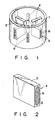
- the magnetron anode produced by the method of the invention has an anode cylinder 1, and a plurality of plate-like anode vanes 2 radially extending in the anode cylinder 1.
- the vanes 2 each have an outer end face 4 secured to the inner surface of the cylinder 1 by laser-beam welding.
- Fig. 2 shows one of the vanes 2, in which reference numeral 5 designates the unmelted area, and numeral 6 designates the melt area.
- the unmelted area should be 20-90% of the entire area of the end face 4 and, accordingly, the remaining 80-10% thereof is the weld or melt area 6.
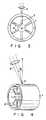
- a plurality of the anode vanes 2 are radially arranged in the anode cylinder 1, and then laser beams 3 are radiated onto the cylinder 1 from the outside, to weld the vanes 2 and the cylinder 1 together, as shown in Figs. 3 and 4.
- a positioning jig not shown, is inserted in the anode cylinder 1, and then a predetermined number of anode vanes 2 are arranged in the same. Thereafter, the anode vanes 2 are urged outwards from the axis of the anode cylinder by the positioning jig against the inner surface of the anode cylinder 1, as is indicated by the arrow F shown in Fig. 3.
- the anodes are arranged such that the diameter D of the circle defined by the respective inner ends of the anode vanes 2, and the angle ⁇ defined by each adjacent pair of vanes 2 attain respective predetermined values. Then, as is shown in Fig.
- the laser beams 3 are radiated at an angle onto the outer periphery of the anode cylinder 1. For example, they are radiated at an angle ⁇ of about 20 degrees with respect to the perpendicular line X. This prevents the laser beams from being reflected from the anode cylinder surface to a laser oscillator, not shown, and hence the power of the laser can be accurately controlled. If the thicknesses of the anode cylinder 1 and the anode vane 2 are each set to 2.0 mm, the diameter of the focal area P of the laser beams 3 is set to 0.2 mm. In relation to this, when copper is used as the component of the members to be welded, carbon-dioxide-gas (CO2) beams, which have a relatively long wavelength, are preferable as the laser beams 3.
- CO2 carbon-dioxide-gas
- the transverse section of the weld is schematically shown in Fig. 5, wherein the melted area 6 extends from the outer peripheral surface of the anode cylinder 1 to the outer end of the anode vane 2, which area is stable physically and mechanically.
- the width W5 of the melted area 6 at the outer surface of the cylinder 1 should be set to 1.2-1.8 mm.
- the unmelted area 5 of the anode vane 2 should be in tight contact with the anode cylinder 1.
- the welding is performed such that the unmelted area 5, having a width W2 of about 0.2 mm, is formed over the peripheral edge of the outer end face 4.
- the unmelted area 5 covers 20% of the entire area of the same, and is in mechanical contact with the anode cylinder 1.
- Fig. 7 shows a variation in the welding, wherein two central portions 6 are welded, each of which has a smaller diameter W3 of about 1 mm and a larger diameter W4 of about 1.5 mm.
- the unmelted area 5 covers substantially 90% of the entire end face 4 of the vane 2. If the unmelted area covers more than 90%, satisfactory welding strength cannot be obtained, while if it covers less than 10%, the melted area 6 becomes too large to fix the vane 2 in position. Consequently, it is preferable to obtain an unmelted area of between 20-90% of the end face 4.
- the vane 2 is sunk in the cylinder 1, resulting in changes in the inner diameter D and/or the angle ⁇ , which are predetermined to desired values.
- the unmelted area 5 is provided in the invention.
- the method of the invention is carried out at room temperature, so that the clearances between the component parts and positioning jig do not change, which enhances the assembling accuracy.
- the method of the invention requires no inserts during welding, which can make the products much cheaper than the conventional ones manufactured by soldering.
Landscapes
- Physics & Mathematics (AREA)
- Optics & Photonics (AREA)
- Engineering & Computer Science (AREA)
- Plasma & Fusion (AREA)
- Mechanical Engineering (AREA)
- Microwave Tubes (AREA)
Applications Claiming Priority (2)
| Application Number | Priority Date | Filing Date | Title |
|---|---|---|---|
| JP1234958A JPH0744006B2 (ja) | 1989-09-11 | 1989-09-11 | マグネトロンアノードの製造方法 |
| JP234958/89 | 1989-09-11 |
Publications (2)
| Publication Number | Publication Date |
|---|---|
| EP0417455A1 true EP0417455A1 (fr) | 1991-03-20 |
| EP0417455B1 EP0417455B1 (fr) | 1994-07-06 |
Family
ID=16978924
Family Applications (1)
| Application Number | Title | Priority Date | Filing Date |
|---|---|---|---|
| EP90114772A Expired - Lifetime EP0417455B1 (fr) | 1989-09-11 | 1990-08-01 | Méthode pour la fabrication d'anodes de magnétron |
Country Status (5)
| Country | Link |
|---|---|
| US (1) | US5078635A (fr) |
| EP (1) | EP0417455B1 (fr) |
| JP (1) | JPH0744006B2 (fr) |
| KR (1) | KR920010171B1 (fr) |
| DE (1) | DE69010433T2 (fr) |
Families Citing this family (1)
| Publication number | Priority date | Publication date | Assignee | Title |
|---|---|---|---|---|
| CN117283176B (zh) * | 2023-10-27 | 2025-03-28 | 中山市美格电子科技有限公司 | 一种磁控管a侧焊接工艺 |
Citations (1)
| Publication number | Priority date | Publication date | Assignee | Title |
|---|---|---|---|---|
| GB2160630A (en) * | 1982-03-11 | 1985-12-24 | Hull Corp | A hollow shelf and a method of manufacture thereof |
Family Cites Families (3)
| Publication number | Priority date | Publication date | Assignee | Title |
|---|---|---|---|---|
| JPS51151060A (en) * | 1975-06-20 | 1976-12-25 | Toshiba Corp | Construction method of a magnetron anode constituted body |
| US4167662A (en) * | 1978-03-27 | 1979-09-11 | National Research Development Corporation | Methods and apparatus for cutting and welding |
| JPS56156646A (en) * | 1980-05-01 | 1981-12-03 | Toshiba Corp | Magnetron anode and manufacture |
-
1989
- 1989-09-11 JP JP1234958A patent/JPH0744006B2/ja not_active Expired - Lifetime
-
1990
- 1990-08-01 EP EP90114772A patent/EP0417455B1/fr not_active Expired - Lifetime
- 1990-08-01 DE DE69010433T patent/DE69010433T2/de not_active Expired - Fee Related
- 1990-08-07 US US07/563,619 patent/US5078635A/en not_active Expired - Lifetime
- 1990-09-11 KR KR1019900014604A patent/KR920010171B1/ko not_active Expired
Patent Citations (1)
| Publication number | Priority date | Publication date | Assignee | Title |
|---|---|---|---|---|
| GB2160630A (en) * | 1982-03-11 | 1985-12-24 | Hull Corp | A hollow shelf and a method of manufacture thereof |
Non-Patent Citations (1)
| Title |
|---|
| PATENT ABSTRACTS OF JAPAN vol. 6, no. 37 (E-097) 06 March 1982, & JP-A-56 156646 (TOSHIBA CORP.) 03 December 1981, * |
Also Published As
| Publication number | Publication date |
|---|---|
| DE69010433D1 (de) | 1994-08-11 |
| DE69010433T2 (de) | 1994-12-22 |
| KR920010171B1 (ko) | 1992-11-19 |
| US5078635A (en) | 1992-01-07 |
| JPH0744006B2 (ja) | 1995-05-15 |
| KR910007053A (ko) | 1991-04-30 |
| EP0417455B1 (fr) | 1994-07-06 |
| JPH0398242A (ja) | 1991-04-23 |
Similar Documents
| Publication | Publication Date | Title |
|---|---|---|
| US5143590A (en) | Method of manufacturing sputtering target assembly | |
| US6765173B2 (en) | Laser welding jig | |
| US5222651A (en) | Process for producing a vacuum interrupter chamber | |
| US5090613A (en) | Method of manufacturing an anode assembly of a magnetron | |
| EP0214611B1 (fr) | Anode de magnétron et méthode de fabrication d'une telle anode | |
| EP0417455A1 (fr) | Méthode pour la fabrication d'anodes de magnétron | |
| CA1085933A (fr) | Mode de fabrication et de raccordement des elements conducteurs de guides d'ondes | |
| JP2005085750A (ja) | 電子レンジ用のマグネトロン及びその形成方法 | |
| CN118371844A (zh) | 用于处理导电端子的方法和电气组件 | |
| JP2538864B2 (ja) | マグネトロンの陽極構体およびその製造方法 | |
| US4486510A (en) | Method of manufacturing tuner chassis | |
| KR102547141B1 (ko) | 브레이징 공법을 이용한 마그네트론 제조방법 | |
| JP3774267B2 (ja) | ろう付け方法 | |
| JPH03272546A (ja) | マグネトロンアノードの製造方法 | |
| JP2695164B2 (ja) | マグネトロン陽極構体 | |
| JPS60160542A (ja) | マグネトロン陽極構体の製造方法 | |
| JPS63143721A (ja) | マグネトロン陽極の製造方法 | |
| KR0132201Y1 (ko) | 마그네트론의 출력부 조립용지그 | |
| JPH0684472A (ja) | マグネトロンの陽極構体及びその製造方法 | |
| JPH0268834A (ja) | マグネトロンの製造方法 | |
| JP2806237B2 (ja) | チップインダクタの製造法 | |
| RU1798071C (ru) | Способ пайки графита с металлом | |
| JPS59184436A (ja) | マグネトロン陽極構体 | |
| JPS59184437A (ja) | マグネトロン陽極構体 | |
| JPS57200762A (en) | Manufacturing method of twin cylinder with lining |
Legal Events
| Date | Code | Title | Description |
|---|---|---|---|
| PUAI | Public reference made under article 153(3) epc to a published international application that has entered the european phase |
Free format text: ORIGINAL CODE: 0009012 |
|
| 17P | Request for examination filed |
Effective date: 19900829 |
|
| AK | Designated contracting states |
Kind code of ref document: A1 Designated state(s): DE FR GB |
|
| 17Q | First examination report despatched |
Effective date: 19930222 |
|
| GRAA | (expected) grant |
Free format text: ORIGINAL CODE: 0009210 |
|
| AK | Designated contracting states |
Kind code of ref document: B1 Designated state(s): DE FR GB |
|
| REF | Corresponds to: |
Ref document number: 69010433 Country of ref document: DE Date of ref document: 19940811 |
|
| ET | Fr: translation filed | ||
| PLBE | No opposition filed within time limit |
Free format text: ORIGINAL CODE: 0009261 |
|
| STAA | Information on the status of an ep patent application or granted ep patent |
Free format text: STATUS: NO OPPOSITION FILED WITHIN TIME LIMIT |
|
| 26N | No opposition filed | ||
| REG | Reference to a national code |
Ref country code: GB Ref legal event code: 746 Effective date: 19981023 |
|
| REG | Reference to a national code |
Ref country code: FR Ref legal event code: D6 |
|
| REG | Reference to a national code |
Ref country code: GB Ref legal event code: IF02 |
|
| PGFP | Annual fee paid to national office [announced via postgrant information from national office to epo] |
Ref country code: DE Payment date: 20080814 Year of fee payment: 19 |
|
| PGFP | Annual fee paid to national office [announced via postgrant information from national office to epo] |
Ref country code: FR Payment date: 20080818 Year of fee payment: 19 |
|
| PGFP | Annual fee paid to national office [announced via postgrant information from national office to epo] |
Ref country code: GB Payment date: 20080813 Year of fee payment: 19 |
|
| GBPC | Gb: european patent ceased through non-payment of renewal fee |
Effective date: 20090801 |
|
| REG | Reference to a national code |
Ref country code: FR Ref legal event code: ST Effective date: 20100430 |
|
| PG25 | Lapsed in a contracting state [announced via postgrant information from national office to epo] |
Ref country code: FR Free format text: LAPSE BECAUSE OF NON-PAYMENT OF DUE FEES Effective date: 20090831 Ref country code: DE Free format text: LAPSE BECAUSE OF NON-PAYMENT OF DUE FEES Effective date: 20100302 |
|
| PG25 | Lapsed in a contracting state [announced via postgrant information from national office to epo] |
Ref country code: GB Free format text: LAPSE BECAUSE OF NON-PAYMENT OF DUE FEES Effective date: 20090801 |