EP0407202A2 - Fabrication de dispositifs-semi-conducteurs - Google Patents
Fabrication de dispositifs-semi-conducteurs Download PDFInfo
- Publication number
- EP0407202A2 EP0407202A2 EP90307377A EP90307377A EP0407202A2 EP 0407202 A2 EP0407202 A2 EP 0407202A2 EP 90307377 A EP90307377 A EP 90307377A EP 90307377 A EP90307377 A EP 90307377A EP 0407202 A2 EP0407202 A2 EP 0407202A2
- Authority
- EP
- European Patent Office
- Prior art keywords
- film
- annealing
- substrate
- silicide layer
- silicon
- Prior art date
- Legal status (The legal status is an assumption and is not a legal conclusion. Google has not performed a legal analysis and makes no representation as to the accuracy of the status listed.)
- Withdrawn
Links
- 239000004065 semiconductor Substances 0.000 title claims abstract description 24
- 238000004519 manufacturing process Methods 0.000 title claims abstract description 15
- 238000000137 annealing Methods 0.000 claims abstract description 40
- 238000000034 method Methods 0.000 claims abstract description 40
- 239000000758 substrate Substances 0.000 claims abstract description 31
- 229910021332 silicide Inorganic materials 0.000 claims abstract description 26
- FVBUAEGBCNSCDD-UHFFFAOYSA-N silicide(4-) Chemical compound [Si-4] FVBUAEGBCNSCDD-UHFFFAOYSA-N 0.000 claims abstract description 26
- XUIMIQQOPSSXEZ-UHFFFAOYSA-N Silicon Chemical compound [Si] XUIMIQQOPSSXEZ-UHFFFAOYSA-N 0.000 claims abstract description 23
- 229910052710 silicon Inorganic materials 0.000 claims abstract description 22
- 239000010703 silicon Substances 0.000 claims abstract description 22
- 229910052751 metal Inorganic materials 0.000 claims abstract description 19
- 239000002184 metal Substances 0.000 claims abstract description 19
- 150000003377 silicon compounds Chemical class 0.000 claims abstract description 19
- 239000010936 titanium Substances 0.000 claims description 14
- VYPSYNLAJGMNEJ-UHFFFAOYSA-N Silicium dioxide Chemical compound O=[Si]=O VYPSYNLAJGMNEJ-UHFFFAOYSA-N 0.000 claims description 12
- RTAQQCXQSZGOHL-UHFFFAOYSA-N Titanium Chemical compound [Ti] RTAQQCXQSZGOHL-UHFFFAOYSA-N 0.000 claims description 11
- 229910052719 titanium Inorganic materials 0.000 claims description 11
- 238000005530 etching Methods 0.000 claims description 7
- 238000001039 wet etching Methods 0.000 claims description 5
- 229910052681 coesite Inorganic materials 0.000 claims 1
- 229910052906 cristobalite Inorganic materials 0.000 claims 1
- 239000000377 silicon dioxide Substances 0.000 claims 1
- 235000012239 silicon dioxide Nutrition 0.000 claims 1
- 229910052682 stishovite Inorganic materials 0.000 claims 1
- 229910052905 tridymite Inorganic materials 0.000 claims 1
- 229910052814 silicon oxide Inorganic materials 0.000 description 10
- 229910021341 titanium silicide Inorganic materials 0.000 description 7
- 229910008479 TiSi2 Inorganic materials 0.000 description 6
- DFJQEGUNXWZVAH-UHFFFAOYSA-N bis($l^{2}-silanylidene)titanium Chemical compound [Si]=[Ti]=[Si] DFJQEGUNXWZVAH-UHFFFAOYSA-N 0.000 description 6
- QVGXLLKOCUKJST-UHFFFAOYSA-N atomic oxygen Chemical compound [O] QVGXLLKOCUKJST-UHFFFAOYSA-N 0.000 description 5
- 239000001301 oxygen Substances 0.000 description 5
- 229910052760 oxygen Inorganic materials 0.000 description 5
- 125000006850 spacer group Chemical group 0.000 description 5
- GWEVSGVZZGPLCZ-UHFFFAOYSA-N Titan oxide Chemical compound O=[Ti]=O GWEVSGVZZGPLCZ-UHFFFAOYSA-N 0.000 description 4
- 238000009826 distribution Methods 0.000 description 4
- 239000012535 impurity Substances 0.000 description 4
- 230000004888 barrier function Effects 0.000 description 3
- 238000009792 diffusion process Methods 0.000 description 3
- XKRFYHLGVUSROY-UHFFFAOYSA-N Argon Chemical compound [Ar] XKRFYHLGVUSROY-UHFFFAOYSA-N 0.000 description 2
- OAICVXFJPJFONN-UHFFFAOYSA-N Phosphorus Chemical compound [P] OAICVXFJPJFONN-UHFFFAOYSA-N 0.000 description 2
- 238000005229 chemical vapour deposition Methods 0.000 description 2
- 238000010276 construction Methods 0.000 description 2
- 238000005516 engineering process Methods 0.000 description 2
- 229910052698 phosphorus Inorganic materials 0.000 description 2
- 239000011574 phosphorus Substances 0.000 description 2
- 238000001020 plasma etching Methods 0.000 description 2
- 238000004544 sputter deposition Methods 0.000 description 2
- VHUUQVKOLVNVRT-UHFFFAOYSA-N Ammonium hydroxide Chemical compound [NH4+].[OH-] VHUUQVKOLVNVRT-UHFFFAOYSA-N 0.000 description 1
- 229910009871 Ti5Si3 Inorganic materials 0.000 description 1
- UGACIEPFGXRWCH-UHFFFAOYSA-N [Si].[Ti] Chemical compound [Si].[Ti] UGACIEPFGXRWCH-UHFFFAOYSA-N 0.000 description 1
- 239000004411 aluminium Substances 0.000 description 1
- 229910052782 aluminium Inorganic materials 0.000 description 1
- XAGFODPZIPBFFR-UHFFFAOYSA-N aluminium Chemical compound [Al] XAGFODPZIPBFFR-UHFFFAOYSA-N 0.000 description 1
- QGZKDVFQNNGYKY-UHFFFAOYSA-N ammonia Natural products N QGZKDVFQNNGYKY-UHFFFAOYSA-N 0.000 description 1
- 229910052786 argon Inorganic materials 0.000 description 1
- 229910052785 arsenic Inorganic materials 0.000 description 1
- RQNWIZPPADIBDY-UHFFFAOYSA-N arsenic atom Chemical compound [As] RQNWIZPPADIBDY-UHFFFAOYSA-N 0.000 description 1
- 230000015572 biosynthetic process Effects 0.000 description 1
- 230000003247 decreasing effect Effects 0.000 description 1
- 230000007812 deficiency Effects 0.000 description 1
- 230000002950 deficient Effects 0.000 description 1
- 238000007872 degassing Methods 0.000 description 1
- 230000005684 electric field Effects 0.000 description 1
- 230000005669 field effect Effects 0.000 description 1
- 238000002955 isolation Methods 0.000 description 1
- 229910044991 metal oxide Inorganic materials 0.000 description 1
- 150000004706 metal oxides Chemical class 0.000 description 1
- 229910021420 polycrystalline silicon Inorganic materials 0.000 description 1
- 230000000750 progressive effect Effects 0.000 description 1
- 230000000630 rising effect Effects 0.000 description 1
Images


Classifications
-
- H—ELECTRICITY
- H01—ELECTRIC ELEMENTS
- H01L—SEMICONDUCTOR DEVICES NOT COVERED BY CLASS H10
- H01L21/00—Processes or apparatus adapted for the manufacture or treatment of semiconductor or solid state devices or of parts thereof
- H01L21/02—Manufacture or treatment of semiconductor devices or of parts thereof
- H01L21/04—Manufacture or treatment of semiconductor devices or of parts thereof the devices having potential barriers, e.g. a PN junction, depletion layer or carrier concentration layer
- H01L21/18—Manufacture or treatment of semiconductor devices or of parts thereof the devices having potential barriers, e.g. a PN junction, depletion layer or carrier concentration layer the devices having semiconductor bodies comprising elements of Group IV of the Periodic Table or AIIIBV compounds with or without impurities, e.g. doping materials
- H01L21/28—Manufacture of electrodes on semiconductor bodies using processes or apparatus not provided for in groups H01L21/20 - H01L21/268
- H01L21/283—Deposition of conductive or insulating materials for electrodes conducting electric current
- H01L21/285—Deposition of conductive or insulating materials for electrodes conducting electric current from a gas or vapour, e.g. condensation
- H01L21/28506—Deposition of conductive or insulating materials for electrodes conducting electric current from a gas or vapour, e.g. condensation of conductive layers
- H01L21/28512—Deposition of conductive or insulating materials for electrodes conducting electric current from a gas or vapour, e.g. condensation of conductive layers on semiconductor bodies comprising elements of Group IV of the Periodic Table
- H01L21/28518—Deposition of conductive or insulating materials for electrodes conducting electric current from a gas or vapour, e.g. condensation of conductive layers on semiconductor bodies comprising elements of Group IV of the Periodic Table the conductive layers comprising silicides
Definitions
- This invention relates to the manufacture of semiconductor devices.
- silicide self aligned silicide
- a metal silicide film is formed on a diffused layer and a gate electrode to decrease the sheet resistance thereof.
- a method of forming a silicide layer on a diffused layer is disclosed, for example, in Japanese Patent Application Publication No. JP-A-63-8U06U.
- a field insulating film 102 such as a silicon oxide (SiO2) film, is selectively formed on portions of a P-type silicon substrate 101 for effecting isolation between various elements.
- a gate insulating film 103 such as a thermally grown SiO2 film, is formed on the surface of an active region between the field insulating portions 102.
- a polycrystalline silicon film is formed on the surface of the gate insulating film 103 by a chemical vapour deposition (CVD) process, after which impurities such as phosphorus (P) are doped into the polycrystalline film to decrease the resistance thereof.
- CVD chemical vapour deposition
- the polycrystalline film is then etched in a desired pattern to form a gate electrode 104 atop the insulating film 103.
- N-type impurities for example phosphorus
- RIE reactive ion etching
- N-type impurities such as arsenic (As) are implanted at high concentration into the silicon substrate 101 with the side wall spacers 105 acting as a mask, annealing then being performed to electrically activate the implanted impurities.
- As arsenic
- the above step forms an N+ type source region 106 and a drain region 107 which are self-aligned relative to the gate electrode 104.
- An N-channel MOSFET metal oxide semiconductor field effect transistor
- the MOSFET comprising the gate electrode 104, the source region 106 and the drain region 107.
- the source and drain regions 106 and 107 will have lightly doped N-type regions 106a and 107a at positions under the side wall spacers 105.
- the N-channel MOSFET has a so-called LDD (Lightly Doped Drain) structure in which the lightly doped region 107a moderates the electric field near to the drain region 107.
- a titanium film is formed over the entire surfaces of the above-mentioned elements by a sputtering process.
- An annealing process is then performed at 600 o C in an atmosphere of argon (Ar) to react the Ti film where it contacts the gate electrode 104, the source region 106 and the drain region 107.
- This process converts surface portions of the gate electrode 104, the source region 106 and the drain region 107 into a silicide layer.
- titanium silicide (TiSi) films 109a, 109b and 109c are formed on the surfaces of the gate electrode 104, the source region 106 and the drain region 107, respectively.
- the unreacted Ti film is removed using a wet etching process.
- the TiSi films 109a, 109b and 109c can decrease the sheet resistances of the gate electrode 104, the source region 106 and the drain region 107.
- the silicide forming technique described above has a disadvantage in that silicon atoms may 'ooze into' the side wall spacers 105 through the silicon substrate 101, so that an undesired TiSi film 109d (shown by a broken line in Figure 1) is formed on the side wall spacer 105, the film not being removable by post etching. This results in an electrical short circuit between the gate electrode 104 and the drain region 107, which phenomenon reduces production efficiency and is responsible for a high number of defective LSIs (low process yield).
- a method of manufacturing a semiconductor device comprising the steps of: forming a film of a silicon compound on a silicon substrate; the silicon compound film having a thickness of less than 50 angstroms; forming a metal film on the silicon compound film; and annealing the substrate, the silicon film and the metal film at a temperature sufficiently high to form a silicide layer on the substrate.
- a method of manufacturing a semiconductor device comprising the steps of: selectively forming a film of a silicon compound on areas of a silicon substrate; forming a second film of the silicon compound over the selectively formed film and substrate, the second film having a thickness of less than 50 angstroms; forming a metal film on the second film; performing a first annealing on the substrate, the silicon film and the metal film; performing a second annealing on the substrate, the silicon film and the metal film, the second annealing being performed at a higher temperature than the first annealing for forming a silicide layer on the substrate.
- a semiconductor device comprising: a silicon substrate; a film of a silicon compound selectively formed on areas of the substrate; a silicide layer selectively formed between the selectively formed areas of said film, the silicide layer having been formed by annealing a silicon compound layer having a thickness of less than 50 angstroms and a metal film, and the silicide layer having a sheet resistance substantially equal to 4 ohms per square.
- the preferred embodiment provides a method of manufacturing a semiconductor device in which a low resistance value metal silicide film may be selectively formed on a predetermined portion of a silicon substrate, and which has high reliability.
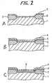
- FIG 2A shows a silicon substrate 1 on which a SiO2 field insulating film 2 has been selectively formed.
- Another SiO2 film 3 having a thickness of less than 50 angstroms, is then formed over the exposed surface of the silicon substrate 1 and the field insulating film 2. This film promotes reaction with an overlaying titanium layer.
- the SiO2 film 3 is formed so as to be thicker than 50 angstroms, for example 100 angstroms, diffusion will not occur sufficiently during a subsequent annealing and etching process and the oxygen and titanium distribution throughout a TiSi2 barrier layer thereby formed will be insufficient.
- the SiO2 film 3 is formed to have a thickness of less than 50 angstroms, at which thickness sufficient diffusion will occur.
- a titanium (Ti) film 4 having a thickness of 400 angstroms, is formed over the entire surface of the previously applied SiO2 film 3 using, for example, a sputtering process.
- low temperature lamp annealing rapid annealing
- a silicon compound reacts with a metal.
- the present low temperature annealing process is for forming a titanium silicide film 5 as shown in Figure 2C.
- the titanium silicide film 5 comprises Ti5Si3 and TiSi, and the titanium film 4 is oxidised into TiO2 against the titanium silicide film 5.
- the remaining unreacted titanium film in and the TiO2 is then removed by way of a wet etching process using aqueous ammonia or the like.
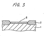
- the titanium silicide film 5 is converted into a TiSi2 film 6 ( Figure 3) by performing a second annealing (high temperature annealing) at 900 o C.
- a second annealing high temperature annealing
- the TiSi2 that is formed has a high resistance value, substantially equal to 3 ohms per square, because of oxygen remaining in the TiSi2 film 6.
- the second annealing is carried out at substantially 900 o C, which can degas the remaining oxygen in the TiSi2 film 6, thus giving the film a lower resistance value of 4 ohms per square.
- the semiconductor device formed by the present method which device is shown in Figure 3, may be formed so as to have a structure significantly simpler than conventional devices, whereby manufacturing reliability is improved.
- efficient degassing of oxygen is carried out in the silicide layer, thereby providing a semiconductor device with a low resistance value.
- the silicide layer of low resistance value can effectively improve the characteristics of a transistor device.
- the preferred semiconductor manufacturing method embodying the invention can effectively form a silicide layer with high selectivity, and with no rising, allowing formation of transistors with decreased leakage current characteristics.
- semiconductor device is a transistor
- methods embodying the invention may be readily applied to the manufacture of other semiconductor devices including various MOS LSIs, bipolar LSIs and bipolar CMOS LSIs.
- the low temperature annealing is carried out at 600 o C in the above embodiment, it is possible to select the low temperature annealing temperature to lie in a range of from 600 o C to 700 o C.
- the high temperature annealing may alternatively be performed at temperatures in a range of from 800 o to 1000 o C, depending on the characteristics desired.
Landscapes
- Engineering & Computer Science (AREA)
- Physics & Mathematics (AREA)
- Condensed Matter Physics & Semiconductors (AREA)
- General Physics & Mathematics (AREA)
- Manufacturing & Machinery (AREA)
- Computer Hardware Design (AREA)
- Microelectronics & Electronic Packaging (AREA)
- Power Engineering (AREA)
- Electrodes Of Semiconductors (AREA)
- Insulated Gate Type Field-Effect Transistor (AREA)
Applications Claiming Priority (2)
| Application Number | Priority Date | Filing Date | Title |
|---|---|---|---|
| JP1175105A JP2910064B2 (ja) | 1989-07-06 | 1989-07-06 | 半導体装置の製造方法 |
| JP175105/89 | 1989-07-06 |
Publications (2)
| Publication Number | Publication Date |
|---|---|
| EP0407202A2 true EP0407202A2 (fr) | 1991-01-09 |
| EP0407202A3 EP0407202A3 (en) | 1992-10-28 |
Family
ID=15990348
Family Applications (1)
| Application Number | Title | Priority Date | Filing Date |
|---|---|---|---|
| EP19900307377 Withdrawn EP0407202A3 (en) | 1989-07-06 | 1990-07-05 | Manufacturing semiconductor devices |
Country Status (2)
| Country | Link |
|---|---|
| EP (1) | EP0407202A3 (fr) |
| JP (1) | JP2910064B2 (fr) |
Cited By (2)
| Publication number | Priority date | Publication date | Assignee | Title |
|---|---|---|---|---|
| WO2002097895A2 (fr) * | 2001-05-26 | 2002-12-05 | Ihp Gmbh-Innovations For High Performance Microelectronics / Institut Für Innovative Mikroelektronik | Transistor, procede de production d'un circuit integre et procede de production d'une couche de silicium metallique |
| US7310262B2 (en) * | 2005-08-22 | 2007-12-18 | Sony Corporation | Ferroelectric memory capable of continuously fast transferring data words in a pipeline |
Families Citing this family (2)
| Publication number | Priority date | Publication date | Assignee | Title |
|---|---|---|---|---|
| US5399526A (en) * | 1991-06-28 | 1995-03-21 | Sony Corporation | Method of manufacturing semiconductor device by forming barrier metal layer between substrate and wiring layer |
| JP2001358089A (ja) * | 2001-05-10 | 2001-12-26 | Oki Electric Ind Co Ltd | 半導体装置の製造方法 |
Citations (3)
| Publication number | Priority date | Publication date | Assignee | Title |
|---|---|---|---|---|
| FR2524709A1 (fr) * | 1982-03-31 | 1983-10-07 | Nippon Telegraph & Telephone | Dispositif a semi-conducteur et procede pour sa fabrication |
| US4551908A (en) * | 1981-06-15 | 1985-11-12 | Nippon Electric Co., Ltd. | Process of forming electrodes and interconnections on silicon semiconductor devices |
| EP0305147A1 (fr) * | 1987-08-24 | 1989-03-01 | THORN EMI North America Inc. | Procédé de fabrication de contact semi-conducteur |
-
1989
- 1989-07-06 JP JP1175105A patent/JP2910064B2/ja not_active Expired - Fee Related
-
1990
- 1990-07-05 EP EP19900307377 patent/EP0407202A3/en not_active Withdrawn
Patent Citations (3)
| Publication number | Priority date | Publication date | Assignee | Title |
|---|---|---|---|---|
| US4551908A (en) * | 1981-06-15 | 1985-11-12 | Nippon Electric Co., Ltd. | Process of forming electrodes and interconnections on silicon semiconductor devices |
| FR2524709A1 (fr) * | 1982-03-31 | 1983-10-07 | Nippon Telegraph & Telephone | Dispositif a semi-conducteur et procede pour sa fabrication |
| EP0305147A1 (fr) * | 1987-08-24 | 1989-03-01 | THORN EMI North America Inc. | Procédé de fabrication de contact semi-conducteur |
Non-Patent Citations (2)
| Title |
|---|
| EXTENDED ABSTRACTS. vol. 87-1, no. 1, 1987, PRINCETON, NEW JERSEY US page 342; LI ET AL.: 'Selective Titanium Silicide Formation by NH3 Plasma Assisted Thermal Silicidation' Abstract No. 238 * |
| THIN SOLID FILMS. vol. 64, no. 3, December 1979, LAUSANNE CH pages 439 - 444; MAA ET AL.: 'Backscattering Analysis of the Successive Layer Structures of Titanium Silicides' * |
Cited By (4)
| Publication number | Priority date | Publication date | Assignee | Title |
|---|---|---|---|---|
| WO2002097895A2 (fr) * | 2001-05-26 | 2002-12-05 | Ihp Gmbh-Innovations For High Performance Microelectronics / Institut Für Innovative Mikroelektronik | Transistor, procede de production d'un circuit integre et procede de production d'une couche de silicium metallique |
| WO2002097895A3 (fr) * | 2001-05-26 | 2003-09-25 | Ihp Gmbh | Transistor, procede de production d'un circuit integre et procede de production d'une couche de silicium metallique |
| US7196382B2 (en) | 2001-05-26 | 2007-03-27 | Ihp Gmbh Innovations For High Performance Microelectronics/ Institut Fur Innovative Mikroelektronik | Transistor, method for producing an integrated circuit and a method of producing a metal silicide layer |
| US7310262B2 (en) * | 2005-08-22 | 2007-12-18 | Sony Corporation | Ferroelectric memory capable of continuously fast transferring data words in a pipeline |
Also Published As
| Publication number | Publication date |
|---|---|
| JPH0338823A (ja) | 1991-02-19 |
| JP2910064B2 (ja) | 1999-06-23 |
| EP0407202A3 (en) | 1992-10-28 |
Similar Documents
| Publication | Publication Date | Title |
|---|---|---|
| JP3285934B2 (ja) | 半導体装置の製造方法 | |
| US4727038A (en) | Method of fabricating semiconductor device | |
| KR100530401B1 (ko) | 저저항 게이트 전극을 구비하는 반도체 장치 | |
| US5268590A (en) | CMOS device and process | |
| US5103272A (en) | Semiconductor device and a method for manufacturing the same | |
| JPH0870053A (ja) | 半導体装置の製造方法 | |
| US5384285A (en) | Process for fabricating a silicide layer in a semiconductor device | |
| US5194405A (en) | Method of manufacturing a semiconductor device having a silicide layer | |
| KR19980053694A (ko) | Mosfet 제조 방법 | |
| KR100376235B1 (ko) | 반도체장치및그제조방법 | |
| EP0404372A2 (fr) | Procédé pour la fabrication de contacts en silicium polycristallin | |
| US5654241A (en) | Method for manufacturing a semiconductor device having reduced resistance of diffusion layers and gate electrodes | |
| JPS6298642A (ja) | 半導体集積回路装置の製造方法 | |
| EP0407202A2 (fr) | Fabrication de dispositifs-semi-conducteurs | |
| JPH0766146A (ja) | 半導体装置の製造方法 | |
| US5989996A (en) | Method for manufacturing semiconductor device | |
| JPH0684824A (ja) | 半導体装置の製造方法 | |
| JP3011941B2 (ja) | 半導体装置の製造方法 | |
| JP3185235B2 (ja) | 半導体装置の製造方法 | |
| JPH07263682A (ja) | サリサイド構造を有するmosfetの製造方法 | |
| JPH06196687A (ja) | 半導体装置の製造方法 | |
| JPH0521458A (ja) | 半導体装置およびその製造方法 | |
| KR100403321B1 (ko) | 반도체소자의제조방법 | |
| JPH11214328A (ja) | 半導体装置及びその製造方法 | |
| JP2748532B2 (ja) | 半導体装置およびその製造方法 |
Legal Events
| Date | Code | Title | Description |
|---|---|---|---|
| PUAI | Public reference made under article 153(3) epc to a published international application that has entered the european phase |
Free format text: ORIGINAL CODE: 0009012 |
|
| AK | Designated contracting states |
Kind code of ref document: A2 Designated state(s): DE FR GB |
|
| PUAL | Search report despatched |
Free format text: ORIGINAL CODE: 0009013 |
|
| AK | Designated contracting states |
Kind code of ref document: A3 Designated state(s): DE FR GB |
|
| 17P | Request for examination filed |
Effective date: 19930330 |
|
| 17Q | First examination report despatched |
Effective date: 19941114 |
|
| APAB | Appeal dossier modified |
Free format text: ORIGINAL CODE: EPIDOS NOAPE |
|
| APAB | Appeal dossier modified |
Free format text: ORIGINAL CODE: EPIDOS NOAPE |
|
| APAD | Appeal reference recorded |
Free format text: ORIGINAL CODE: EPIDOS REFNE |
|
| STAA | Information on the status of an ep patent application or granted ep patent |
Free format text: STATUS: THE APPLICATION IS DEEMED TO BE WITHDRAWN |
|
| 18D | Application deemed to be withdrawn |
Effective date: 20030201 |
|
| APAF | Appeal reference modified |
Free format text: ORIGINAL CODE: EPIDOSCREFNE |