EP0406814A2 - Encapsulation par aspersion de modules photovoltaiques - Google Patents
Encapsulation par aspersion de modules photovoltaiques Download PDFInfo
- Publication number
- EP0406814A2 EP0406814A2 EP90112714A EP90112714A EP0406814A2 EP 0406814 A2 EP0406814 A2 EP 0406814A2 EP 90112714 A EP90112714 A EP 90112714A EP 90112714 A EP90112714 A EP 90112714A EP 0406814 A2 EP0406814 A2 EP 0406814A2
- Authority
- EP
- European Patent Office
- Prior art keywords
- photovoltaic module
- mixture
- exposed surface
- photovoltaic
- superstrate
- Prior art date
- Legal status (The legal status is an assumption and is not a legal conclusion. Google has not performed a legal analysis and makes no representation as to the accuracy of the status listed.)
- Granted
Links
- 239000007921 spray Substances 0.000 title description 5
- 238000005538 encapsulation Methods 0.000 title 1
- 239000000203 mixture Substances 0.000 claims abstract description 23
- 238000000576 coating method Methods 0.000 claims abstract description 22
- 238000002955 isolation Methods 0.000 claims abstract description 22
- 239000011248 coating agent Substances 0.000 claims abstract description 21
- 230000004888 barrier function Effects 0.000 claims abstract description 18
- 238000000034 method Methods 0.000 claims abstract description 14
- BPSIOYPQMFLKFR-UHFFFAOYSA-N trimethoxy-[3-(oxiran-2-ylmethoxy)propyl]silane Chemical compound CO[Si](OC)(OC)CCCOCC1CO1 BPSIOYPQMFLKFR-UHFFFAOYSA-N 0.000 claims abstract description 14
- 239000004814 polyurethane Substances 0.000 claims abstract description 10
- 229920002635 polyurethane Polymers 0.000 claims abstract description 10
- 239000010410 layer Substances 0.000 claims description 19
- ZWEHNKRNPOVVGH-UHFFFAOYSA-N 2-Butanone Chemical compound CCC(C)=O ZWEHNKRNPOVVGH-UHFFFAOYSA-N 0.000 claims description 9
- 238000010438 heat treatment Methods 0.000 claims description 6
- 239000002356 single layer Substances 0.000 claims description 4
- 239000002904 solvent Substances 0.000 claims description 4
- 238000005507 spraying Methods 0.000 claims description 4
- 239000007795 chemical reaction product Substances 0.000 claims description 2
- 239000008393 encapsulating agent Substances 0.000 description 23
- 238000012360 testing method Methods 0.000 description 17
- 239000000463 material Substances 0.000 description 7
- 238000009413 insulation Methods 0.000 description 6
- 229910000077 silane Inorganic materials 0.000 description 6
- XLYOFNOQVPJJNP-UHFFFAOYSA-N water Substances O XLYOFNOQVPJJNP-UHFFFAOYSA-N 0.000 description 6
- 230000015556 catabolic process Effects 0.000 description 5
- 239000011247 coating layer Substances 0.000 description 5
- 238000005260 corrosion Methods 0.000 description 5
- 230000007797 corrosion Effects 0.000 description 5
- 239000000356 contaminant Substances 0.000 description 4
- 230000007613 environmental effect Effects 0.000 description 4
- 238000007654 immersion Methods 0.000 description 4
- BLRPTPMANUNPDV-UHFFFAOYSA-N Silane Chemical group [SiH4] BLRPTPMANUNPDV-UHFFFAOYSA-N 0.000 description 3
- 238000003916 acid precipitation Methods 0.000 description 3
- XAGFODPZIPBFFR-UHFFFAOYSA-N aluminium Chemical compound [Al] XAGFODPZIPBFFR-UHFFFAOYSA-N 0.000 description 3
- 229910052782 aluminium Inorganic materials 0.000 description 3
- 230000000694 effects Effects 0.000 description 3
- BFMKFCLXZSUVPI-UHFFFAOYSA-N ethyl but-3-enoate Chemical compound CCOC(=O)CC=C BFMKFCLXZSUVPI-UHFFFAOYSA-N 0.000 description 3
- 239000011521 glass Substances 0.000 description 3
- 229920000642 polymer Polymers 0.000 description 3
- -1 silane compound Chemical class 0.000 description 3
- XOLBLPGZBRYERU-UHFFFAOYSA-N tin dioxide Chemical compound O=[Sn]=O XOLBLPGZBRYERU-UHFFFAOYSA-N 0.000 description 3
- JOYRKODLDBILNP-UHFFFAOYSA-N Ethyl urethane Chemical compound CCOC(N)=O JOYRKODLDBILNP-UHFFFAOYSA-N 0.000 description 2
- 238000010420 art technique Methods 0.000 description 2
- 238000004132 cross linking Methods 0.000 description 2
- 238000006731 degradation reaction Methods 0.000 description 2
- 230000007246 mechanism Effects 0.000 description 2
- 230000004048 modification Effects 0.000 description 2
- 238000012986 modification Methods 0.000 description 2
- 230000009257 reactivity Effects 0.000 description 2
- 229910000679 solder Inorganic materials 0.000 description 2
- 229940008841 1,6-hexamethylene diisocyanate Drugs 0.000 description 1
- SVONRAPFKPVNKG-UHFFFAOYSA-N 2-ethoxyethyl acetate Chemical compound CCOCCOC(C)=O SVONRAPFKPVNKG-UHFFFAOYSA-N 0.000 description 1
- 240000008881 Oenanthe javanica Species 0.000 description 1
- BQCADISMDOOEFD-UHFFFAOYSA-N Silver Chemical compound [Ag] BQCADISMDOOEFD-UHFFFAOYSA-N 0.000 description 1
- 238000005299 abrasion Methods 0.000 description 1
- NIXOWILDQLNWCW-UHFFFAOYSA-N acrylic acid group Chemical group C(C=C)(=O)O NIXOWILDQLNWCW-UHFFFAOYSA-N 0.000 description 1
- 230000009471 action Effects 0.000 description 1
- 239000000853 adhesive Substances 0.000 description 1
- 230000001070 adhesive effect Effects 0.000 description 1
- 239000002390 adhesive tape Substances 0.000 description 1
- 229920000180 alkyd Polymers 0.000 description 1
- 229910021417 amorphous silicon Inorganic materials 0.000 description 1
- 150000001875 compounds Chemical class 0.000 description 1
- 239000004020 conductor Substances 0.000 description 1
- 239000007822 coupling agent Substances 0.000 description 1
- 238000000151 deposition Methods 0.000 description 1
- 238000001035 drying Methods 0.000 description 1
- 238000005516 engineering process Methods 0.000 description 1
- 238000005530 etching Methods 0.000 description 1
- RRAMGCGOFNQTLD-UHFFFAOYSA-N hexamethylene diisocyanate Chemical compound O=C=NCCCCCCN=C=O RRAMGCGOFNQTLD-UHFFFAOYSA-N 0.000 description 1
- 239000012943 hotmelt Substances 0.000 description 1
- 125000002887 hydroxy group Chemical group [H]O* 0.000 description 1
- 238000010030 laminating Methods 0.000 description 1
- 238000003475 lamination Methods 0.000 description 1
- 238000002156 mixing Methods 0.000 description 1
- 229920000058 polyacrylate Polymers 0.000 description 1
- 229920000728 polyester Polymers 0.000 description 1
- 229920002620 polyvinyl fluoride Polymers 0.000 description 1
- 239000000047 product Substances 0.000 description 1
- 230000001681 protective effect Effects 0.000 description 1
- 229910052709 silver Inorganic materials 0.000 description 1
- 239000004332 silver Substances 0.000 description 1
- 239000004094 surface-active agent Substances 0.000 description 1
- 239000008399 tap water Substances 0.000 description 1
- 235000020679 tap water Nutrition 0.000 description 1
- 238000010998 test method Methods 0.000 description 1
- 229910001887 tin oxide Inorganic materials 0.000 description 1
- 230000007704 transition Effects 0.000 description 1
Images

Classifications
-
- H—ELECTRICITY
- H01—ELECTRIC ELEMENTS
- H01L—SEMICONDUCTOR DEVICES NOT COVERED BY CLASS H10
- H01L31/00—Semiconductor devices sensitive to infrared radiation, light, electromagnetic radiation of shorter wavelength or corpuscular radiation and specially adapted either for the conversion of the energy of such radiation into electrical energy or for the control of electrical energy by such radiation; Processes or apparatus specially adapted for the manufacture or treatment thereof or of parts thereof; Details thereof
- H01L31/04—Semiconductor devices sensitive to infrared radiation, light, electromagnetic radiation of shorter wavelength or corpuscular radiation and specially adapted either for the conversion of the energy of such radiation into electrical energy or for the control of electrical energy by such radiation; Processes or apparatus specially adapted for the manufacture or treatment thereof or of parts thereof; Details thereof adapted as photovoltaic [PV] conversion devices
- H01L31/042—PV modules or arrays of single PV cells
- H01L31/0445—PV modules or arrays of single PV cells including thin film solar cells, e.g. single thin film a-Si, CIS or CdTe solar cells
- H01L31/046—PV modules composed of a plurality of thin film solar cells deposited on the same substrate
-
- H—ELECTRICITY
- H01—ELECTRIC ELEMENTS
- H01L—SEMICONDUCTOR DEVICES NOT COVERED BY CLASS H10
- H01L29/00—Semiconductor devices adapted for rectifying, amplifying, oscillating or switching, or capacitors or resistors with at least one potential-jump barrier or surface barrier, e.g. PN junction depletion layer or carrier concentration layer; Details of semiconductor bodies or of electrodes thereof ; Multistep manufacturing processes therefor
-
- H—ELECTRICITY
- H01—ELECTRIC ELEMENTS
- H01L—SEMICONDUCTOR DEVICES NOT COVERED BY CLASS H10
- H01L31/00—Semiconductor devices sensitive to infrared radiation, light, electromagnetic radiation of shorter wavelength or corpuscular radiation and specially adapted either for the conversion of the energy of such radiation into electrical energy or for the control of electrical energy by such radiation; Processes or apparatus specially adapted for the manufacture or treatment thereof or of parts thereof; Details thereof
- H01L31/04—Semiconductor devices sensitive to infrared radiation, light, electromagnetic radiation of shorter wavelength or corpuscular radiation and specially adapted either for the conversion of the energy of such radiation into electrical energy or for the control of electrical energy by such radiation; Processes or apparatus specially adapted for the manufacture or treatment thereof or of parts thereof; Details thereof adapted as photovoltaic [PV] conversion devices
- H01L31/042—PV modules or arrays of single PV cells
- H01L31/0475—PV cell arrays made by cells in a planar, e.g. repetitive, configuration on a single semiconductor substrate; PV cell microarrays
-
- H—ELECTRICITY
- H01—ELECTRIC ELEMENTS
- H01L—SEMICONDUCTOR DEVICES NOT COVERED BY CLASS H10
- H01L31/00—Semiconductor devices sensitive to infrared radiation, light, electromagnetic radiation of shorter wavelength or corpuscular radiation and specially adapted either for the conversion of the energy of such radiation into electrical energy or for the control of electrical energy by such radiation; Processes or apparatus specially adapted for the manufacture or treatment thereof or of parts thereof; Details thereof
- H01L31/04—Semiconductor devices sensitive to infrared radiation, light, electromagnetic radiation of shorter wavelength or corpuscular radiation and specially adapted either for the conversion of the energy of such radiation into electrical energy or for the control of electrical energy by such radiation; Processes or apparatus specially adapted for the manufacture or treatment thereof or of parts thereof; Details thereof adapted as photovoltaic [PV] conversion devices
- H01L31/042—PV modules or arrays of single PV cells
- H01L31/048—Encapsulation of modules
-
- Y—GENERAL TAGGING OF NEW TECHNOLOGICAL DEVELOPMENTS; GENERAL TAGGING OF CROSS-SECTIONAL TECHNOLOGIES SPANNING OVER SEVERAL SECTIONS OF THE IPC; TECHNICAL SUBJECTS COVERED BY FORMER USPC CROSS-REFERENCE ART COLLECTIONS [XRACs] AND DIGESTS
- Y02—TECHNOLOGIES OR APPLICATIONS FOR MITIGATION OR ADAPTATION AGAINST CLIMATE CHANGE
- Y02E—REDUCTION OF GREENHOUSE GAS [GHG] EMISSIONS, RELATED TO ENERGY GENERATION, TRANSMISSION OR DISTRIBUTION
- Y02E10/00—Energy generation through renewable energy sources
- Y02E10/50—Photovoltaic [PV] energy
Definitions
- the present invention relates to encapsulants for photovoltaic modules and, more particularly, to spray encapsulants for photovoltaic modules and also relates to a photovoltaic module having a wide isolation scribe.
- Photovoltaic modules include a superstrate of, for example, glass upon which one or more photovoltaic cells are fabricated.
- the photovoltaic cells are connected in series and a solder pad is conventionally provided at either end of the series of photovoltaic cells to which power leads can be attached.
- photovoltaic modules can also be protected by isolation scribes, which are rectangular grooves located around the perimeter of photovoltaic modules to protect the module from contaminants.
- encapsulants exist in a variety of forms such as a rigid glass panel laminated to the photovoltaic cells with an adhesive as disclosed by U.S. Patent No. 4,331,494 to Duchateau et al. , or an acrylic polymer pottant and weather resistant layer as disclosed in U.S. Patent No. 4,374,955 to Gupta et al .
- Photovoltaic modules also have been encapsulated by acrylic prepolymers that are cast on the photovoltaic cells and cured to form an encapsulant as disclosed by U.S. Patent No. 4,549,033 to Avenel et al .
- a photovoltaic module may also be encapsulated by laminating a layer of Tedlar® (manufactured and available from E.I. DuPont de Nemours & Co. of Wilmington, Delaware) to the exposed side of the photovoltaic cells with a layer of ethyl vinyl acetate (EVA) (designated herein as "EVA lamination”).
- EVA ethyl vinyl acetate
- Another conventional encapsulant is a coating on the exposed side of the photovoltaic cells of ultraviolet (UV) curable urethane (designated herein as "UV urethane”).
- UV ultraviolet
- prior art photovoltaic modules typically utilized two narrow isolation scribes around the perimeter of the photovoltaic module. Such an arrangement suffers from problems of buildup of particulates in the scribe lines with resultant loss of effectiveness of the scribes. Moreover, it is difficult and costly to produce photovoltaic modules with narrow isolation scribes.
- the present invention overcomes the problems and disadvantages of the prior art by providing a photovoltaic module encapsulant that is inexpensive, is easily applied and provides superior protection against potentially harmful ambient conditions. Further, the photovoltaic module of the invention preferably includes an isolation scribe that is easy to fabricate and provides protection against environmental contaminants.
- the present invention provides a method of encapsulating a photovoltaic module.
- the photovoltaic module to be encapsulated has an exposed surface and includes a superstrate and one or more photovoltaic cells disposed on the superstrate.
- the method of the present invention includes the steps of mixing a two component fluorinated polyurethane material with 3-glycidoxy propyltrimethoxy silane, applying the mixture onto the exposed surface of the photovoltaic module, heating the photovoltaic module at a first temperature for a time sufficient to dry the mixture and heating the photovoltaic module at a second temperature for a time sufficient to cure the mixture.
- the coating material of the present invention is preferivelyably applied by spraying onto the exposed surface of the module.
- the coating may be dried at a temperature ranging from 50° to 90°C and then may be cured at a temperature preferably ranging from 80° to 150°C and more preferably at a temperature ranging from 90° to 130°C.
- the coating thickness preferably ranges from 1.0 to 3.0 mils dry film thickness and more preferably ranges from 1.8 to 2.2 mils dry film thickness.
- the coating material of the invention may be applied in a single layer, or alternatively, may be applied in two or more layers.
- an encapsulated photovoltaic module that includes a superstrate and one or more photovoltaic cells disposed thereon.
- the one or more photovoltaic cells has an exposed surface.
- the exposed surface of the one or more photovoltaic cells contains a two component barrier coating.
- This barrier coating comprises the reaction product of a fluorinated polyurethane material mixed together with 3-glycidoxypropyltrimethoxy silane.
- the barrier coating mixture may also contain a solvent such as methyl ethyl ketone.
- the amount of the 3-glycidoxypropyltrimethoxy silane in the barrier coating mixture preferively ranges from 1.0% to 2.0% by weight.
- the photovoltaic module also preferably includes an isolation scribe located around the perimeter of the module.
- the isolation scribe is preferably 5-8 microns in width.
- a method for encapsulating a photovoltaic module.
- the photovoltaic module includes a superstrate and one or more photovoltaic cells.
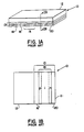
- a conventional photovoltaic module is provided that includes, a superstrate 12 of, for example glass, and a photovoltaic cell assembly 13 that includes one or more photovoltaic cells 14 connected in series.
- Photovoltaic cell assembly 13 is referred to herein as "cell assembly 13".
- photovoltaic module 10 of Fig. 1A shows four individual photovoltaic cells 14 connected in series on superstrate 12. As more clearly shown in Fig.
- cell assembly 13 is fabricated on superstrate 12 by depositing a first conductor 16 of, for example, tin oxide (S n O2), a layer 18 of amorphous silicon and a second or back contact layer 20 of, for example, aluminum.
- a surface 21 of back contact layer 20 is exposed to ambient conditions.
- Surface 21 is referred to herein as the "exposed surface of the photovoltaic module" or simply the “exposed surface.”
- cell assembly 13 does include such layers as previously described.
- insulation pads 22 are disposed on cell assembly 13. Insulation pads 22 preferably include a silver frit buss bar which enables an electrical connection to be formed at each end of a photovoltaic module.
- the present invention provides a spray encapsulant for application to the exposed surface of the photovoltaic module.
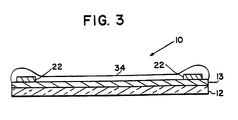
- Fig. 3 illustrates a photovoltaic module 10 including a spray encapsulant or barrier coating 34 applied to the exposed surface of the module.
- a mixture of a two component fluorinated polyurethane with 3-glycidoxy propyltrimethoxy silane can be applied to the exposed surface of the one or more photovoltaic cells.
- the two component fluorinated polyurethane is preferably CPU 66/3 (available from KRC Research Corp., Moorestown, N.J.) which is a 5:1 mixture of
- the encapsulant of the invention comprising a mixture of a two component fluorinated polyurethane with 3-glycidoxy propyltrimethoxy silane also functions to protect the photovoltaic module from mechanisms other than galvanic corrosion.
- the encapsulant can protect the module from acid rain which is capable, by the action of HCl, of etching back contact layer 20 of the photovoltaic module.
- the encapsulant of the invention can protect the module from scratches and other harmful abrasions.
- the encapsulant of the invention is preferably sprayed onto the photovoltaic module by use of, for example, an air type spray gun.
- a stationary hand-type gun or an automated spraying system may be utilized.
- the preferred amount of 3-glycidoxy propyltrimethoxy silane in the mixture ranges from 1.0% to 2.0% by weight.
- the mixture may also include a solvent, such as methyl ethyl ketone.
- the mixture may be applied in a single layer or may be applied in two or more layers. After application of a coating layer of encapsulant, the layer may be heated to a temperature preferably ranging from 50° to 90°C to dry the layer.
- the drying step may range from 10 to 30 minutes, whereas due to increased efficiency, a shorter period will be sufficient when utilizing an automated system.
- the coating layer can then be heated to a temperature preferably ranging from 80° to 150°C and more preferably to a temperature ranging from 90° to 130°C to cure the layer.
- the curing step may range from 10 to 30 minutes for a hand sprayer and less for an automated sprayer.
- the final dry film thickness of the encapsulant layer prefer strictlyably ranges from 1.0 to 3.0 mils and more preferably ranges from 1.8 to 2.2 mils.
- the mechanism of curing is believed to consist of the silane compound crosslinking with the fluorinated polyurethane compound.
- the silane compound bonds with the aluminum of the exposed surface of the photovoltaic module.
- the aluminum of the exposed surface of the photovoltaic module is hydrated, i.e., is characterized by the presence of hydroxyl groups at the surface, and the silane compound is believed to react with these AlOH surface groups.
- the encapsulant may be applied to the photovoltaic module prior to attachment of electrical connections to insulation pads 22. If this is the case, a maskant may be applied to insulation pads 22 to protect them from the barrier coating or the coating may be removed around insulation pads 22 prior to attachment of the electrical connections. Alternatively, the electrical connections may be attached to insulation pads 22 and masked prior to application of the encapsulant.
- an isolation scribe 30 is preferably located around the perimeter of back contact layer 20 of photovoltaic module 10.
- the purpose of isolation scribe 30 is to coact with the encapsulant 32 to further protect the module from acid rain, moisture and other contaminants to prevent galvanic corrosion.
- the encapsulant that is disposed in scribe 30 acts as a wall or a barrier to the propagation of moisture or other contaminants in a direction parallel to the exposed surface of the photovoltaic module.
- the encapsulant of the invention has a high dielectric strength which, because of the direct correlation between isolation scribe width and the electrical breakdown voltage of the module, enables a wide isolation scribe 30 to be utilized while still achieving the desired breakdown voltage. Therefore, isolation scribe 30 can be made wider than those scribes of the prior art without resulting breakdown voltage problems.
- Prior art isolation scribes usually range from 1-2 mils in width.
- Isolation scribe 30 preferably has a width ranging from 5 to 8 mils.
- the wider scribe provides a greater barrier against moisture, is more easily cleaned and is easier to fabricate than the narrower scribes typically utilized by the prior art.
- the combination of the wider isolation scribe and the application of an encapsulant barrier coating acts to effectively protect the photovoltaic module from galvanic corrosion caused by ambient conditions.
- modules were coated with a barrier coating containing 1% by weight of 3-glycidoxy-propyltrimethoxy silane mixed with CPU 66/3 which is a two-component fluorinated polyurethane material available from KRC Research Corp., Moorestown, New Jersey.
- the coating was applied in a single layer by utilizing an Integrated Technologies Automated Spraying System utilizing eight (8) respirating guns.
- the coating layer was applied to a thickness of 4 mils wet.
- the modules were then placed on a conveyor belt and transported through an oven consisting of an initial flash zone (five feet long) followed by five heating zones (each two feet in length). The entire oven length was 15 feet.
- the temperatures in heating zones 1-5 were 50°C, 75°C, 100°C, 100°C and 120°C, respectively.
- the modules were conveyed through the oven at a rate of 1 foot/minute.
- the final dry film thickness of the coating layer was 2.0 mils.
- the coated modules underwent several different environmental tests. All 16 had wide (5-8 mils) isolation scribes and wires soldered to them with hot melt over the solder joints.
- the 16 modules were divided into 3 groups. Group 1 underwent thermal cycle and humidity freeze tests. Group 2 underwent a water immersion test and group 3 underwent humidity soak and wet isolation tests.
- T.C. testing was conducted in an environmental enclosure which maintains a dry temperature cycle of +90°C to -40°C; 4 cycles a day with a 45-minute transition period between cycles. The test was run for 12.5 days.
- the humidity freeze (H.F.) testing was conducted in an environmental enclosure which maintained 85% humidity throughout the test.
- the temperature cycle was +85°C for 20 hours to -40°C for 1-2 hours.
- the test ran for 10 days.
- VOLTAGE AVERAGE Pm (volts) Initial 11.77 2.45 After T.C. 11.93 2.60 After H.F. 11.90 2.63 (Pm-maximum power) The modules did not degrade as a result of this testing.
- Water immersion was conducted by immersing the modules in water heated to 50°C for 5 days with an ELH lamp.
- the ELH lamp is manufactured by and available from GTE Sylvania Products Corp. of Salem, Massachusetts.
- the modules were electrically tested after testing for degradation.
- Humidity soak testing was conducted in an environmental enclosure with a humidity of 85% and a temperature of 85°C. The test was 30 days long.
- the modules leaked at .020 to .030 mA. (The modules fail if the leak is .040 mA or more).
- modules prepared according to the invention will last for 21 to 28 days on the average without a significant loss in power.
Applications Claiming Priority (2)
| Application Number | Priority Date | Filing Date | Title |
|---|---|---|---|
| US07/375,954 US4953577A (en) | 1989-07-06 | 1989-07-06 | Spray encapsulation of photovoltaic modules |
| US375954 | 1989-07-06 |
Publications (3)
| Publication Number | Publication Date |
|---|---|
| EP0406814A2 true EP0406814A2 (fr) | 1991-01-09 |
| EP0406814A3 EP0406814A3 (en) | 1992-03-18 |
| EP0406814B1 EP0406814B1 (fr) | 1995-03-22 |
Family
ID=23483062
Family Applications (1)
| Application Number | Title | Priority Date | Filing Date |
|---|---|---|---|
| EP90112714A Expired - Lifetime EP0406814B1 (fr) | 1989-07-06 | 1990-07-03 | Encapsulation par aspersion de modules photovoltaiques |
Country Status (9)
| Country | Link |
|---|---|
| US (1) | US4953577A (fr) |
| EP (1) | EP0406814B1 (fr) |
| JP (1) | JPH03116788A (fr) |
| KR (1) | KR940002767B1 (fr) |
| CN (1) | CN1023740C (fr) |
| AT (1) | ATE120309T1 (fr) |
| CA (1) | CA2020241A1 (fr) |
| DE (1) | DE69017963T2 (fr) |
| ES (1) | ES2072942T3 (fr) |
Cited By (4)
| Publication number | Priority date | Publication date | Assignee | Title |
|---|---|---|---|---|
| EP0755079A3 (fr) * | 1995-07-19 | 1999-03-10 | Canon Kabushiki Kaisha | Matériau protecteur pour un élément semi-conducteur, élément semi-conducteur pourvu de ce matériau protecteur et dispositif semi-conducteur pourvu de cet élément semi-conducteur |
| EP1005096A2 (fr) * | 1998-11-12 | 2000-05-31 | Kaneka Corporation | Module de cellules solaires |
| WO2005006451A1 (fr) | 2003-07-07 | 2005-01-20 | Dow Corning Corporation | Encapsulation de piles solaires |
| US9812600B2 (en) | 2012-03-27 | 2017-11-07 | Covestro Deutschland Ag | Use of UV-radiation-hardenable polyurethane resins for producing solar laminates |
Families Citing this family (26)
| Publication number | Priority date | Publication date | Assignee | Title |
|---|---|---|---|---|
| US5164020A (en) * | 1991-05-24 | 1992-11-17 | Solarex Corporation | Solar panel |
| US5507880A (en) * | 1992-06-08 | 1996-04-16 | Kanegafuchi Kagaku Kogyo Kabushiki Kaisha | Amorphous solar module having improved passivation |
| US5470396A (en) * | 1994-04-12 | 1995-11-28 | Amoco Corporation | Solar cell module package and method for its preparation |
| JP3397443B2 (ja) * | 1994-04-30 | 2003-04-14 | キヤノン株式会社 | 太陽電池モジュール及びその製造方法 |
| US5487792A (en) * | 1994-06-13 | 1996-01-30 | Midwest Research Institute | Molecular assemblies as protective barriers and adhesion promotion interlayer |
| US5637156A (en) * | 1994-09-22 | 1997-06-10 | Semiconductor Energy Laboratory Co., Ltd. | Resin Composition and an electronic device using the same |
| US6525261B1 (en) | 1994-09-22 | 2003-02-25 | Semiconductor Energy Laboratory Co., Ltd. | Resin composition and an electronic device using the same |
| US6077722A (en) * | 1998-07-14 | 2000-06-20 | Bp Solarex | Producing thin film photovoltaic modules with high integrity interconnects and dual layer contacts |
| US20050178428A1 (en) * | 2004-02-17 | 2005-08-18 | Solar Roofing Systems Inc. | Photovoltaic system and method of making same |
| US7910822B1 (en) | 2005-10-17 | 2011-03-22 | Solaria Corporation | Fabrication process for photovoltaic cell |
| US8227688B1 (en) | 2005-10-17 | 2012-07-24 | Solaria Corporation | Method and resulting structure for assembling photovoltaic regions onto lead frame members for integration on concentrating elements for solar cells |
| AU2006349274B2 (en) * | 2006-10-09 | 2013-08-22 | S.I.E.M. S.R.L. | Process for manufacturing combined solar panels of photovoltaic and thermal type and related solar panel |
| US20090056806A1 (en) * | 2007-09-05 | 2009-03-05 | Solaria Corporation | Solar cell structure including a plurality of concentrator elements with a notch design and predetermined radii and method |
| US7910392B2 (en) | 2007-04-02 | 2011-03-22 | Solaria Corporation | Method and system for assembling a solar cell package |
| US8119902B2 (en) | 2007-05-21 | 2012-02-21 | Solaria Corporation | Concentrating module and method of manufacture for photovoltaic strips |
| DE102007038240B4 (de) | 2007-08-13 | 2013-02-07 | Institut für Kunststofftechnologie und -recycling e.V. | Verfahren und Anlage zur Herstellung eines Solarmoduls |
| US7910035B2 (en) | 2007-12-12 | 2011-03-22 | Solaria Corporation | Method and system for manufacturing integrated molded concentrator photovoltaic device |
| US20100101561A1 (en) * | 2008-10-24 | 2010-04-29 | Christopher Frank | Solar panels systems and methods |
| US20100294341A1 (en) * | 2008-10-24 | 2010-11-25 | Christopher Frank | Apparatus and methods for frameless building integrated photovoltaic panel |
| DE102009026026A1 (de) * | 2009-06-24 | 2010-12-30 | Malibu Gmbh & Co. Kg | Photovoltaikmodul und Verfahren zu dessen Herstellung |
| US8362357B2 (en) * | 2009-11-24 | 2013-01-29 | Nesbitt Jeffrey E | Environmentally-friendly coatings and environmentally-friendly systems and methods for generating energy |
| US20130056065A1 (en) * | 2010-06-07 | 2013-03-07 | E I Duont De Nemours and Company | Transparent film containing tetrafluoroethylene-hexafluoropropylene copolymer and having an organosilane coupling agent treated surface |
| CN102315311A (zh) * | 2010-07-06 | 2012-01-11 | 杜邦太阳能有限公司 | 太阳能模块装置及其封边涂布方法 |
| CN102694059A (zh) * | 2011-03-23 | 2012-09-26 | 晶城科技有限公司 | 太阳能芯片封装工艺 |
| USD699176S1 (en) | 2011-06-02 | 2014-02-11 | Solaria Corporation | Fastener for solar modules |
| CN114429996B (zh) * | 2020-10-29 | 2024-03-08 | 苏州阿特斯阳光电力科技有限公司 | 光伏组件及其制造工艺 |
Citations (7)
| Publication number | Priority date | Publication date | Assignee | Title |
|---|---|---|---|---|
| FR2394895A1 (fr) * | 1977-06-16 | 1979-01-12 | Bfg Glassgroup | Panneau de captage de l'energie solaire et procede de fabrication d'un panneau feuillete de captage de l'energie solaire |
| JPS56100676A (en) * | 1980-01-17 | 1981-08-12 | Sumitomo Electric Ind Ltd | Fluorine-base resin coating method |
| JPS5717137A (en) * | 1980-07-04 | 1982-01-28 | Mitsubishi Electric Corp | Manufacture of semiconductor element |
| FR2501213A1 (fr) * | 1981-03-05 | 1982-09-10 | Altulor Sa | Prepolymere acrylique et son application a l'encapsulation de photopiles |
| US4374955A (en) * | 1980-06-11 | 1983-02-22 | California Institute Of Technology | N-Butyl acrylate polymer composition for solar cell encapsulation and method |
| FR2515874A1 (fr) * | 1981-11-05 | 1983-05-06 | Comp Generale Electricite | Procede d'encapsulation plastique de cellules solaires |
| US4692557A (en) * | 1986-10-16 | 1987-09-08 | Shell Oil Company | Encapsulated solar cell assemblage and method of making |
Family Cites Families (22)
| Publication number | Priority date | Publication date | Assignee | Title |
|---|---|---|---|---|
| US4317844A (en) * | 1975-07-28 | 1982-03-02 | Rca Corporation | Semiconductor device having a body of amorphous silicon and method of making the same |
| US4064521A (en) * | 1975-07-28 | 1977-12-20 | Rca Corporation | Semiconductor device having a body of amorphous silicon |
| US4217148A (en) * | 1979-06-18 | 1980-08-12 | Rca Corporation | Compensated amorphous silicon solar cell |
| DE2940917A1 (de) * | 1979-10-09 | 1981-04-23 | Wacker-Chemie GmbH, 8000 München | Klebstoffe |
| US4292092A (en) * | 1980-06-02 | 1981-09-29 | Rca Corporation | Laser processing technique for fabricating series-connected and tandem junction series-connected solar cells into a solar battery |
| US4383129A (en) * | 1980-06-11 | 1983-05-10 | California Institute Of Technology | Solar cell encapsulation |
| US4529829A (en) * | 1982-11-24 | 1985-07-16 | Semiconductor Energy Laboratory Co., Ltd. | Photoelectric conversion device |
| JPS59201471A (ja) * | 1983-04-29 | 1984-11-15 | Semiconductor Energy Lab Co Ltd | 光電変換半導体装置 |
| US4592925A (en) * | 1982-12-20 | 1986-06-03 | Hughes Aircraft Company | Polyimide composition and method for protecting photoreactive cells |
| DE3312053C2 (de) * | 1983-04-02 | 1985-03-28 | Nukem Gmbh, 6450 Hanau | Verfahren zum Verhindern von Kurz- oder Nebenschlüssen in einer großflächigen Dünnschicht-Solarzelle |
| JPS59198773A (ja) * | 1983-04-25 | 1984-11-10 | Shimizu Constr Co Ltd | 太陽電池 |
| JPS59198776A (ja) * | 1983-04-26 | 1984-11-10 | Fuji Electric Corp Res & Dev Ltd | 太陽電池モジユ−ル |
| JPS603164A (ja) * | 1983-06-21 | 1985-01-09 | Sanyo Electric Co Ltd | 光起電力装置の製造方法 |
| US4499658A (en) * | 1983-09-06 | 1985-02-19 | Atlantic Richfield Company | Solar cell laminates |
| US4568409A (en) * | 1983-11-17 | 1986-02-04 | Chronar Corp. | Precision marking of layers |
| US4542257A (en) * | 1984-04-27 | 1985-09-17 | Hughes Aircraft Company | Solar cell array panel and method of manufacture |
| US4636578A (en) * | 1985-04-11 | 1987-01-13 | Atlantic Richfield Company | Photocell assembly |
| DE3542116A1 (de) * | 1985-11-28 | 1987-06-04 | Nukem Gmbh | Photovoltaische zelle |
| JPS639159A (ja) * | 1986-06-30 | 1988-01-14 | Matsushita Electric Ind Co Ltd | 太陽電池モジユ−ル |
| US4860509A (en) * | 1987-05-18 | 1989-08-29 | Laaly Heshmat O | Photovoltaic cells in combination with single ply roofing membranes |
| US4773944A (en) * | 1987-09-08 | 1988-09-27 | Energy Conversion Devices, Inc. | Large area, low voltage, high current photovoltaic modules and method of fabricating same |
| US4830038A (en) * | 1988-01-20 | 1989-05-16 | Atlantic Richfield Company | Photovoltaic module |
-
1989
- 1989-07-06 US US07/375,954 patent/US4953577A/en not_active Expired - Fee Related
-
1990
- 1990-06-29 CA CA002020241A patent/CA2020241A1/fr not_active Abandoned
- 1990-06-29 KR KR1019900009732A patent/KR940002767B1/ko not_active IP Right Cessation
- 1990-07-03 DE DE69017963T patent/DE69017963T2/de not_active Expired - Fee Related
- 1990-07-03 AT AT90112714T patent/ATE120309T1/de not_active IP Right Cessation
- 1990-07-03 EP EP90112714A patent/EP0406814B1/fr not_active Expired - Lifetime
- 1990-07-03 ES ES90112714T patent/ES2072942T3/es not_active Expired - Lifetime
- 1990-07-05 CN CN90103350A patent/CN1023740C/zh not_active Expired - Fee Related
- 1990-07-06 JP JP2179418A patent/JPH03116788A/ja active Pending
Patent Citations (7)
| Publication number | Priority date | Publication date | Assignee | Title |
|---|---|---|---|---|
| FR2394895A1 (fr) * | 1977-06-16 | 1979-01-12 | Bfg Glassgroup | Panneau de captage de l'energie solaire et procede de fabrication d'un panneau feuillete de captage de l'energie solaire |
| JPS56100676A (en) * | 1980-01-17 | 1981-08-12 | Sumitomo Electric Ind Ltd | Fluorine-base resin coating method |
| US4374955A (en) * | 1980-06-11 | 1983-02-22 | California Institute Of Technology | N-Butyl acrylate polymer composition for solar cell encapsulation and method |
| JPS5717137A (en) * | 1980-07-04 | 1982-01-28 | Mitsubishi Electric Corp | Manufacture of semiconductor element |
| FR2501213A1 (fr) * | 1981-03-05 | 1982-09-10 | Altulor Sa | Prepolymere acrylique et son application a l'encapsulation de photopiles |
| FR2515874A1 (fr) * | 1981-11-05 | 1983-05-06 | Comp Generale Electricite | Procede d'encapsulation plastique de cellules solaires |
| US4692557A (en) * | 1986-10-16 | 1987-09-08 | Shell Oil Company | Encapsulated solar cell assemblage and method of making |
Non-Patent Citations (2)
| Title |
|---|
| PATENT ABSTRACTS OF JAPAN vol. 5, no. 178 (C-78)14 November 1981 & JP-A-56 100 676 ( SUMITOMO ELECTRIC IND LTD ) 12 August 1981 * |
| PATENT ABSTRACTS OF JAPAN vol. 6, no. 77 (E-106)(955) 14 May 1982 & JP-A-57 017 137 ( MITSUBISHI DENKI KK ) 28 January 1982 * |
Cited By (9)
| Publication number | Priority date | Publication date | Assignee | Title |
|---|---|---|---|---|
| EP0755079A3 (fr) * | 1995-07-19 | 1999-03-10 | Canon Kabushiki Kaisha | Matériau protecteur pour un élément semi-conducteur, élément semi-conducteur pourvu de ce matériau protecteur et dispositif semi-conducteur pourvu de cet élément semi-conducteur |
| EP1005096A2 (fr) * | 1998-11-12 | 2000-05-31 | Kaneka Corporation | Module de cellules solaires |
| EP1005096A3 (fr) * | 1998-11-12 | 2000-12-27 | Kaneka Corporation | Module de cellules solaires |
| US6300556B1 (en) | 1998-11-12 | 2001-10-09 | Kaneka Corporation | Solar cell module |
| US6384315B1 (en) | 1998-11-12 | 2002-05-07 | Kaneka Corporation | Solar cell module |
| WO2005006451A1 (fr) | 2003-07-07 | 2005-01-20 | Dow Corning Corporation | Encapsulation de piles solaires |
| US8847063B2 (en) | 2003-07-07 | 2014-09-30 | Dow Corning Corporation | Encapsulation of solar cells |
| US8847064B2 (en) | 2003-07-07 | 2014-09-30 | Dow Corning Corporation | Encapsulation of solar cells |
| US9812600B2 (en) | 2012-03-27 | 2017-11-07 | Covestro Deutschland Ag | Use of UV-radiation-hardenable polyurethane resins for producing solar laminates |
Also Published As
| Publication number | Publication date |
|---|---|
| CA2020241A1 (fr) | 1991-01-07 |
| KR910003841A (ko) | 1991-02-28 |
| ES2072942T3 (es) | 1995-08-01 |
| US4953577A (en) | 1990-09-04 |
| DE69017963T2 (de) | 1995-07-20 |
| DE69017963D1 (de) | 1995-04-27 |
| CN1049248A (zh) | 1991-02-13 |
| KR940002767B1 (ko) | 1994-04-02 |
| JPH03116788A (ja) | 1991-05-17 |
| EP0406814A3 (en) | 1992-03-18 |
| EP0406814B1 (fr) | 1995-03-22 |
| ATE120309T1 (de) | 1995-04-15 |
| CN1023740C (zh) | 1994-02-09 |
Similar Documents
| Publication | Publication Date | Title |
|---|---|---|
| EP0406814B1 (fr) | Encapsulation par aspersion de modules photovoltaiques | |
| EP1009037B1 (fr) | Module de cellule solaire | |
| US5482571A (en) | Solar cell module | |
| JP3387741B2 (ja) | 半導体素子用保護材、該保護材を有する半導体素子、該素子を有する半導体装置 | |
| US5973258A (en) | Photovoltaic device | |
| US5514627A (en) | Method and apparatus for improving the performance of light emitting diodes | |
| CN1322593C (zh) | 太阳能电池模块和太阳能电池模块阵列 | |
| US8796064B2 (en) | Method and device for producing a solar module comprising flexible thin-film solar cells, and solar module comprising flexible thin-film solar cells | |
| US20150325728A1 (en) | Systems and methods for improved photovoltaic module structure and encapsulation | |
| CN101258611A (zh) | 具有改进的背板的光电模块 | |
| US20090139567A1 (en) | Conformal protective coating for solar panel | |
| US5884868A (en) | Radiator using thermal control coating | |
| CZ20012282A3 (cs) | Solární modul | |
| US20150333207A1 (en) | Systems and methods for improved photovoltaic module structure | |
| EP1470191B1 (fr) | Couche barriere constituee par une resine durcissante contenant un polyol polymere | |
| JP2012518908A (ja) | 改良型光発電モジュール構造体および封入体のためのシステムおよび方法 | |
| EP2395560A2 (fr) | Module de cellule solaire | |
| JP3732073B2 (ja) | 半導体用電極およびその製造方法 | |
| JPH0476229B2 (fr) | ||
| JPH1056191A (ja) | 太陽電池モジュール | |
| JP2002335002A (ja) | 光起電力素子及びその製造方法 | |
| JPS63147377A (ja) | 薄膜太陽電池 | |
| JP2001284615A (ja) | 保護層付き光起電力素子及びその製造方法、太陽電池モジュール及びその製造方法 | |
| JPS60137043A (ja) | 樹脂封止形半導体装置の製造方法 |
Legal Events
| Date | Code | Title | Description |
|---|---|---|---|
| PUAI | Public reference made under article 153(3) epc to a published international application that has entered the european phase |
Free format text: ORIGINAL CODE: 0009012 |
|
| AK | Designated contracting states |
Kind code of ref document: A2 Designated state(s): AT BE CH DE DK ES FR GB GR IT LI LU NL SE |
|
| PUAL | Search report despatched |
Free format text: ORIGINAL CODE: 0009013 |
|
| AK | Designated contracting states |
Kind code of ref document: A3 Designated state(s): AT BE CH DE DK ES FR GB GR IT LI LU NL SE |
|
| 17P | Request for examination filed |
Effective date: 19920917 |
|
| 17Q | First examination report despatched |
Effective date: 19940302 |
|
| GRAA | (expected) grant |
Free format text: ORIGINAL CODE: 0009210 |
|
| AK | Designated contracting states |
Kind code of ref document: B1 Designated state(s): AT BE CH DE DK ES FR GB GR IT LI LU NL SE |
|
| PG25 | Lapsed in a contracting state [announced via postgrant information from national office to epo] |
Ref country code: NL Free format text: LAPSE BECAUSE OF FAILURE TO SUBMIT A TRANSLATION OF THE DESCRIPTION OR TO PAY THE FEE WITHIN THE PRESCRIBED TIME-LIMIT Effective date: 19950322 Ref country code: LI Effective date: 19950322 Ref country code: GR Free format text: LAPSE BECAUSE OF FAILURE TO SUBMIT A TRANSLATION OF THE DESCRIPTION OR TO PAY THE FEE WITHIN THE PRESCRIBED TIME-LIMIT Effective date: 19950322 Ref country code: DK Effective date: 19950322 Ref country code: CH Effective date: 19950322 Ref country code: BE Effective date: 19950322 Ref country code: AT Effective date: 19950322 |
|
| REF | Corresponds to: |
Ref document number: 120309 Country of ref document: AT Date of ref document: 19950415 Kind code of ref document: T |
|
| REF | Corresponds to: |
Ref document number: 69017963 Country of ref document: DE Date of ref document: 19950427 |
|
| ET | Fr: translation filed | ||
| ITF | It: translation for a ep patent filed |
Owner name: PROPRIA PROTEZIONE PROPR. IND. |
|
| PGFP | Annual fee paid to national office [announced via postgrant information from national office to epo] |
Ref country code: FR Payment date: 19950616 Year of fee payment: 6 |
|
| PG25 | Lapsed in a contracting state [announced via postgrant information from national office to epo] |
Ref country code: SE Effective date: 19950622 |
|
| PGFP | Annual fee paid to national office [announced via postgrant information from national office to epo] |
Ref country code: DE Payment date: 19950623 Year of fee payment: 6 |
|
| PGFP | Annual fee paid to national office [announced via postgrant information from national office to epo] |
Ref country code: GB Payment date: 19950628 Year of fee payment: 6 |
|
| REG | Reference to a national code |
Ref country code: CH Ref legal event code: PL |
|
| PGFP | Annual fee paid to national office [announced via postgrant information from national office to epo] |
Ref country code: ES Payment date: 19950712 Year of fee payment: 6 |
|
| PG25 | Lapsed in a contracting state [announced via postgrant information from national office to epo] |
Ref country code: LU Free format text: LAPSE BECAUSE OF NON-PAYMENT OF DUE FEES Effective date: 19950731 |
|
| REG | Reference to a national code |
Ref country code: ES Ref legal event code: FG2A Ref document number: 2072942 Country of ref document: ES Kind code of ref document: T3 |
|
| NLV1 | Nl: lapsed or annulled due to failure to fulfill the requirements of art. 29p and 29m of the patents act | ||
| PLBE | No opposition filed within time limit |
Free format text: ORIGINAL CODE: 0009261 |
|
| STAA | Information on the status of an ep patent application or granted ep patent |
Free format text: STATUS: NO OPPOSITION FILED WITHIN TIME LIMIT |
|
| 26N | No opposition filed | ||
| PG25 | Lapsed in a contracting state [announced via postgrant information from national office to epo] |
Ref country code: GB Effective date: 19960703 |
|
| PG25 | Lapsed in a contracting state [announced via postgrant information from national office to epo] |
Ref country code: ES Free format text: LAPSE BECAUSE OF THE APPLICANT RENOUNCES Effective date: 19960704 |
|
| GBPC | Gb: european patent ceased through non-payment of renewal fee |
Effective date: 19960703 |
|
| PG25 | Lapsed in a contracting state [announced via postgrant information from national office to epo] |
Ref country code: FR Effective date: 19970328 |
|
| PG25 | Lapsed in a contracting state [announced via postgrant information from national office to epo] |
Ref country code: DE Effective date: 19970402 |
|
| REG | Reference to a national code |
Ref country code: FR Ref legal event code: ST |
|
| REG | Reference to a national code |
Ref country code: ES Ref legal event code: FD2A Effective date: 19991007 |
|
| PG25 | Lapsed in a contracting state [announced via postgrant information from national office to epo] |
Ref country code: IT Free format text: LAPSE BECAUSE OF NON-PAYMENT OF DUE FEES Effective date: 20050703 |