EP0404008A2 - Substratvorspannungs-Generatorschaltung für integrierte Halbleiterschaltung - Google Patents
Substratvorspannungs-Generatorschaltung für integrierte Halbleiterschaltung Download PDFInfo
- Publication number
- EP0404008A2 EP0404008A2 EP90111438A EP90111438A EP0404008A2 EP 0404008 A2 EP0404008 A2 EP 0404008A2 EP 90111438 A EP90111438 A EP 90111438A EP 90111438 A EP90111438 A EP 90111438A EP 0404008 A2 EP0404008 A2 EP 0404008A2
- Authority
- EP
- European Patent Office
- Prior art keywords
- substrate
- semiconductor
- integrated circuit
- semiconductor integrated
- substrate bias
- Prior art date
- Legal status (The legal status is an assumption and is not a legal conclusion. Google has not performed a legal analysis and makes no representation as to the accuracy of the status listed.)
- Ceased
Links
- 239000000758 substrate Substances 0.000 title claims abstract description 138
- 239000004065 semiconductor Substances 0.000 title claims abstract description 103
- 239000003990 capacitor Substances 0.000 claims description 12
- 239000000969 carrier Substances 0.000 description 8
- 238000010586 diagram Methods 0.000 description 7
- 230000000694 effects Effects 0.000 description 3
- 238000010521 absorption reaction Methods 0.000 description 2
- 229910052729 chemical element Inorganic materials 0.000 description 2
- 230000006870 function Effects 0.000 description 2
- 230000000295 complement effect Effects 0.000 description 1
- 238000010276 construction Methods 0.000 description 1
- 230000002708 enhancing effect Effects 0.000 description 1
- 230000012447 hatching Effects 0.000 description 1
- 230000010354 integration Effects 0.000 description 1
- 229910044991 metal oxide Inorganic materials 0.000 description 1
- 150000004706 metal oxides Chemical class 0.000 description 1
- 230000003334 potential effect Effects 0.000 description 1
- QHGVXILFMXYDRS-UHFFFAOYSA-N pyraclofos Chemical compound C1=C(OP(=O)(OCC)SCCC)C=NN1C1=CC=C(Cl)C=C1 QHGVXILFMXYDRS-UHFFFAOYSA-N 0.000 description 1
Images

Classifications
-
- G—PHYSICS
- G11—INFORMATION STORAGE
- G11C—STATIC STORES
- G11C11/00—Digital stores characterised by the use of particular electric or magnetic storage elements; Storage elements therefor
- G11C11/21—Digital stores characterised by the use of particular electric or magnetic storage elements; Storage elements therefor using electric elements
- G11C11/34—Digital stores characterised by the use of particular electric or magnetic storage elements; Storage elements therefor using electric elements using semiconductor devices
- G11C11/40—Digital stores characterised by the use of particular electric or magnetic storage elements; Storage elements therefor using electric elements using semiconductor devices using transistors
- G11C11/401—Digital stores characterised by the use of particular electric or magnetic storage elements; Storage elements therefor using electric elements using semiconductor devices using transistors forming cells needing refreshing or charge regeneration, i.e. dynamic cells
- G11C11/4063—Auxiliary circuits, e.g. for addressing, decoding, driving, writing, sensing or timing
- G11C11/407—Auxiliary circuits, e.g. for addressing, decoding, driving, writing, sensing or timing for memory cells of the field-effect type
- G11C11/4074—Power supply or voltage generation circuits, e.g. bias voltage generators, substrate voltage generators, back-up power, power control circuits
-
- G—PHYSICS
- G11—INFORMATION STORAGE
- G11C—STATIC STORES
- G11C5/00—Details of stores covered by group G11C11/00
- G11C5/14—Power supply arrangements, e.g. power down, chip selection or deselection, layout of wirings or power grids, or multiple supply levels
- G11C5/145—Applications of charge pumps; Boosted voltage circuits; Clamp circuits therefor
- G11C5/146—Substrate bias generators
-
- H—ELECTRICITY
- H10—SEMICONDUCTOR DEVICES; ELECTRIC SOLID-STATE DEVICES NOT OTHERWISE PROVIDED FOR
- H10D—INORGANIC ELECTRIC SEMICONDUCTOR DEVICES
- H10D89/00—Aspects of integrated devices not covered by groups H10D84/00 - H10D88/00
- H10D89/211—Design considerations for internal polarisation
- H10D89/213—Design considerations for internal polarisation in field-effect devices
- H10D89/215—Design considerations for internal polarisation in field-effect devices comprising arrangements for charge pumping or biasing substrates
Definitions
- This invention relates to a semiconductor integrated circuit formed on a chip and having a substrate-bias circuit, and more particularly to a substrate bias generation circuit used in a CMOS DRAM (complementary metal oxide semiconductor dynamic random access memory) of relatively large capacity.
- CMOS DRAM complementary metal oxide semiconductor dynamic random access memory
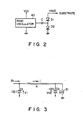
- Fig. 1A is a cross sectional view of a CMOS inverter and Fig. 1B is a circuit diagram of the CMOS inverter.
- element 32 denotes n-type semiconductor well area and element 10 denotes p-type semiconductor substrate.
- impact ionization is a phenomenon in which holes 30 are generated by current I which flows in a channel created by a high level voltage applied to the gate of the N-channel MOS FET.
- a substrate bias generation circuit 11 for negatively biasing the substrate is provided for a memory of relatively large capacity, in order to absorb the holes generated by the impact ionization. That is, a substrate bias voltage Vsub (for example, -2.5 to -3 V) is derived from a power source voltage Vcc (for example, +5 V) applied from the exterior to the chip and an output voltage thereof is applied to the semiconductor substrate.
- the bias circuit includes a ring oscillator, a capacitor C and diodes D1 and D2 as shown in Fig. 2, for example.
- the holes 30 are attracted by the bias circuit 31 and flow in a resistor R of the substrate as a substrate current i.
- the substrate bias generation circuit when used in a dynamic RAM, it functions to prevent the PN junction of an input section being turned on by the undershoot of an input signal and causing a large amount of electrons to be injected into the substrate, destroying data stored in the memory cell.
- Ih denotes a current caused by holes injected into the semiconductor substrate by impact ionization or the like
- R denotes the resistance of the substrate
- 31 denotes the substrate bias generation circuit
- C0 denotes a capacitor near the substrate bias generation circuit
- C1 denotes a capacitor of a circuit positioned at the remotest position from the substrate bias generation circuit
- i denotes a substrate current flowing in the substrate
- ibb denotes an absorption current of the bias circuit.
- a time delay caused by the presence of the capacitors C0 and C1 and the resistor R of the semiconductor substrate may occur in a period from when carriers (for example, holes) are injected into the semiconductor substrate until the carriers are absorbed into the substrate bias generation circuit via the resistor R of the semiconductor substrate.
- the time delay causes the substrate potential at the remotest area from the substrate bias generation circuit to be set to a potential which temporarily deviates from the potential determined by the substrate bias generation circuit.
- the back-gate bias of a MOS transistor lying at the remotest position from the substrate bias generation circuit is temporarily changed. Accordingly, the gate threshold voltage of the MOS transistor is varied. As a result, the noise margin of the circuit is lowered, causing an erroneous operation.
- the MOS transistor which is formed as an enhancement type is changed into a depletion type, setting the circuit into an inoperative condition.
- An object of this invention is to provide a semiconductor integrated circuit, in a high-speed semiconductor memory, in which the substrate potential of an area in which a large amount of current is generated and causes a large amount of charges to be injected into the semiconductor substrate of a group of circuits can be prevented from transiently and locally deviating from a preset value and the MOS transistor of an enhancement type can be prevented from being changed into a depletion type by the back-gate bias effect, for example, so as to prevent the circuit from being set into an inoperative condition.
- a semiconductor integrated circuit which comprises a semiconductor substrate; a semiconductor integrated circuit formed on the semiconductor substrate; a semiconductor chip having the semiconductor substrate and the semiconductor integrated circuit; and a plurality of substrate bias generation circuits dispersedly arranged on the semiconductor chip, derive a substrate bias voltage from a power source voltage supplied from the exterior to the semiconductor chip, and apply the substrate bias voltage to the semiconductor substrate or well area so as to uniformly apply the bias voltage to the semiconductor integrated circuit.
- a plurality of substrate bias generation circuits are arranged in their respective areas of the chip.
- the time constant of a current flowing in the area becomes smaller than the time constant in the prior art case, thereby ensuring that the stability of the substrate potential can be attained on the entire portion of the semiconductor integrated circuit. Therefore, in a semiconductor integrated circuit such as a 4M-bit dynamic RAM which is required to have a large capacity and high operation speed, a stable substrate bias voltage can be applied over the entire portion of the integrated circuit.
- the back-gate bias voltages of MOS transistors formed on the semiconductor substrate will not vary, thereby ensuring a stable transistor operation and significantly enhancing the operation margin of the circuit.
- a stable substrate bias voltage is applied to the entire portion of the semiconductor integrated circuit so that a bipolar action starting voltage characteristic of the PN junction of the semiconductor in the entire portion of the semiconductor integrated circuit can be improved. Therefore, the anti-latch-up characteristic against the undershoot of an input signal can be significantly improved.
- the width of the depletion layer of the PN junction in the entire portion of the semiconductor circuit is enlarged by the substrate bias generation circuit of this invention, thus reducing the capacitance of the PN junction.
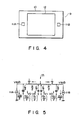
- a substrate bias generation circuit is shown in Fig. 4, wherein a semiconductor chip 9 in which, for example, two substrate bias generation circuits 11A and 11B are arranged on either side of a semiconductor integrated circuit 12 (for example, memory cell array) on a semiconductor substrate 10 of a CMOS dynamic RAM.
- the two substrate bias generation circuits 11A and 11B are arranged in their respective areas, which are calculated by dividing the chip 10 into two substantially equal portions. For example, as shown in Fig.
- the substrate bias generation circuits 11A and 11B are arranged on both sides of the semiconductor integrated circuit 12 which is disposed on substantially the central portion of the semiconductor substrate 10. In this case, it is preferable to arrange the substrate bias generation circuits 11A and 11B so that the distances between the bias circuits and the remotest portions, from the bias circuits, of the respective areas allocated to the bias circuits in the integrated circuit 12 can be equal to each other. As a result, the substrate bias voltage can be substantially uniformly applied over the entire portion of the semiconductor integrated circuit 12.
- MOS transistor which acts as an enhancement type transistor in a normal operation mode (when a normal substrate bias voltage is applied to the semiconductor substrate of the chip) is formed on the semiconductor substrate.
- a circuit group for example, a circuit group such as a data line restore circuit or data output buffer in a dynamic RAM which generates a large current
- the substrate potential of the area can be prevented from transiently and locally deviating from a preset potential.
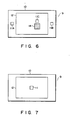
- Fig. 6 shows this case, and a hatching portion 14 indicates the circuit group which generates a large current and 11C denotes a bias generation circuit newly disposed for the circuit group.
- the enhancement type MOS transistor can be prevented from being changed into a depletion type so as to prevent the circuit from being rendered inoperative.
- the time constant of the current flowing in the semiconductor substrate is derived with reference to Figs. 3 and 5.
- R denotes a resistor of the semiconductor substrate
- C0 and C1 respectively denote capacitors provided near the substrate bias generation circuit 31 and in an area of the remotest point from the bias generation circuit 31
- q0 and q1 respectively denote charges stored on the capacitors C0 and C1
- V0 and V1 respectively denote voltages generated across the capacitors C0 and C1
- Ih indicates a current caused by carriers which are generated by the impact ionization or the like and injected into the semiconductor substrate when the circuit group at the remotest area from the substrate bias generation circuit 31 is operated
- Ibb indicates an absorption current of the substrate bias generation circuit
- i indicates a substrate current or a current flowing in the resistor R.
- T0 C ⁇ R/2
- the time constant T0 is a function of the capacitance C and resistance R of the semiconductor substrate.
- C/2 indicates capacitors of the semiconductor substrate which are provided near the substrate bias generation circuits 11A and 11B and at the remotest and substantially the same distant point from the substrate bias generation circuits 11A and 11B
- R/2 indicates the resistor of the semiconductor substrate from the two substrate bias generation circuits 11A and 11B to the remotest point
- q0/2 and V0 respectively denote the amount of charges stored in the capacitor C/2 of the semiconductor substrate provided near the substrate bias generation circuits 11A and 11B and a voltage generated across the capacitor C/2
- Ih indicates carriers (current) which are generated and injected into the semiconductor substrate when the circuit group at the remotest and substantially the same distant area from the substrate bias generation circuits 11A and 11B is operated.
- the above carriers are carriers such as holes which are generated by impact ionization or the like.
- i/2 denotes a substrate current flowing in each of the substrate resistors R/2.
- the two substrate bias generation circuits 11A and 11B are arranged to be allocated equally divided areas of the chip.
- each of the areas of the chip on which substrate bias generation circuits 11A and 11B are disposed has an area substantially one half that of the area on the integrated circuit on which a single substrate bias generation circuit of Fig. 3 is formed.
- the resistance and capacitance of each of the areas on which the substrate bias generation circuits 11A and 11B are respectively arranged are reduced to 1/2, the time constant T of the substrate current i/2 can be reduced to 1/4 of that of a conventional case, thereby significantly improving the stability of the substrate potential.
- substrate bias generation circuits Two or three substrate bias generation circuits are utilized in the above embodiment. However, it is also possible to utilize four or more substrate bias generation circuits, and in this way, the stability of the substrate potential can be further improved. In this case, it is preferable to arrange substrate bias generation circuits on equally divided areas of the integrated circuit 12. That is, it is preferable to uniformly arrange the substrate bias generation circuits such that the distances between the bias circuits and the remotest areas, from the bias circuits, in the area allocated to the bias circuits can be set substantially equal to one another.
- the same effect can be obtained when the substrate bias circuit 11 is arranged at substantially the central portion of the semiconductor integrated circuit 12 to reduce the distance from the bias circuit 11 to the remotest area.
Landscapes
- Engineering & Computer Science (AREA)
- Power Engineering (AREA)
- Microelectronics & Electronic Packaging (AREA)
- Computer Hardware Design (AREA)
- Semiconductor Integrated Circuits (AREA)
- Dram (AREA)
- Semiconductor Memories (AREA)
Applications Claiming Priority (2)
| Application Number | Priority Date | Filing Date | Title |
|---|---|---|---|
| JP156046/89 | 1989-06-19 | ||
| JP1156046A JP2645142B2 (ja) | 1989-06-19 | 1989-06-19 | ダイナミック型ランダムアクセスメモリ |
Publications (2)
| Publication Number | Publication Date |
|---|---|
| EP0404008A2 true EP0404008A2 (de) | 1990-12-27 |
| EP0404008A3 EP0404008A3 (de) | 1992-04-01 |
Family
ID=15619136
Family Applications (1)
| Application Number | Title | Priority Date | Filing Date |
|---|---|---|---|
| EP19900111438 Ceased EP0404008A3 (de) | 1989-06-19 | 1990-06-18 | Substratvorspannungs-Generatorschaltung für integrierte Halbleiterschaltung |
Country Status (4)
| Country | Link |
|---|---|
| US (1) | US5043597A (de) |
| EP (1) | EP0404008A3 (de) |
| JP (1) | JP2645142B2 (de) |
| KR (1) | KR930005498B1 (de) |
Cited By (2)
| Publication number | Priority date | Publication date | Assignee | Title |
|---|---|---|---|---|
| EP0674252A1 (de) * | 1994-03-25 | 1995-09-27 | C.S.E.M. Centre Suisse D'electronique Et De Microtechnique Sa | Schaltung zur Steuerung von Spannungen zwischen Wanne und Source von Transistoren einer logischen MOS-Schaltung und Servosystem zu seiner Leistungsversorgung |
| EP0753892A1 (de) * | 1995-07-11 | 1997-01-15 | Texas Instruments Incorporated | Halbleiteranordnung mit einem Schutzmittel |
Families Citing this family (8)
| Publication number | Priority date | Publication date | Assignee | Title |
|---|---|---|---|---|
| JP2686376B2 (ja) * | 1991-04-03 | 1997-12-08 | 三菱電機株式会社 | 半導体記憶装置 |
| JP3097200B2 (ja) * | 1991-08-26 | 2000-10-10 | 日本電気株式会社 | 半導体装置 |
| EP0564204A3 (en) * | 1992-03-30 | 1994-09-28 | Mitsubishi Electric Corp | Semiconductor device |
| KR950006067Y1 (ko) * | 1992-10-08 | 1995-07-27 | 문정환 | 반도체 메모리 장치 |
| KR0132641B1 (ko) * | 1993-05-25 | 1998-04-16 | 세끼모또 타다히로 | 기판 바이어스 회로 |
| JP2684976B2 (ja) * | 1993-11-24 | 1997-12-03 | 日本電気株式会社 | 半導体装置 |
| JP3732914B2 (ja) * | 1997-02-28 | 2006-01-11 | 株式会社ルネサステクノロジ | 半導体装置 |
| JP4587746B2 (ja) * | 2004-08-30 | 2010-11-24 | 富士通セミコンダクター株式会社 | 半導体装置 |
Family Cites Families (13)
| Publication number | Priority date | Publication date | Assignee | Title |
|---|---|---|---|---|
| JPS5559756A (en) * | 1978-10-30 | 1980-05-06 | Fujitsu Ltd | Semiconductor device |
| JPS5951750B2 (ja) * | 1978-11-24 | 1984-12-15 | 富士通株式会社 | 基板バイアス発生回路 |
| JPS5632758A (en) * | 1979-08-27 | 1981-04-02 | Fujitsu Ltd | Substrate bias generating circuit |
| US4539490A (en) * | 1979-12-08 | 1985-09-03 | Tokyo Shibaura Denki Kabushiki Kaisha | Charge pump substrate bias with antiparasitic guard ring |
| US4433257A (en) * | 1980-03-03 | 1984-02-21 | Tokyo Shibaura Denki Kabushiki Kaisha | Voltage supply for operating a plurality of changing transistors in a manner which reduces minority carrier disruption of adjacent memory cells |
| JPS5758351A (en) * | 1980-09-24 | 1982-04-08 | Toshiba Corp | Substrate biasing device |
| JPS582061A (ja) * | 1981-06-26 | 1983-01-07 | Seiko Epson Corp | Cmos集積回路 |
| EP0093818A1 (de) * | 1982-05-07 | 1983-11-16 | Deutsche ITT Industries GmbH | Monolithisch integrierte Schaltung mit integrierten Kondensatoren |
| US4494223B1 (en) * | 1982-09-16 | 1999-09-07 | Texas Instruments Inc | Sequentially clocked substrate bias generator for dynamic memory |
| NL8402764A (nl) * | 1984-09-11 | 1986-04-01 | Philips Nv | Schakeling voor het opwekken van een substraatvoorspanning. |
| US4686388A (en) * | 1985-03-12 | 1987-08-11 | Pitney Bowes Inc. | Integrated circuit substrate bias selection circuit |
| US4791317A (en) * | 1986-09-26 | 1988-12-13 | Siemens Aktiengesellschaft | Latch-up protection circuit for integrated circuits using complementary mos circuit technology |
| JPH0682781B2 (ja) * | 1987-02-27 | 1994-10-19 | 日本電気株式会社 | 半導体装置 |
-
1989
- 1989-06-19 JP JP1156046A patent/JP2645142B2/ja not_active Expired - Fee Related
-
1990
- 1990-06-14 KR KR1019900008736A patent/KR930005498B1/ko not_active Expired - Lifetime
- 1990-06-18 US US07/539,217 patent/US5043597A/en not_active Expired - Lifetime
- 1990-06-18 EP EP19900111438 patent/EP0404008A3/de not_active Ceased
Cited By (4)
| Publication number | Priority date | Publication date | Assignee | Title |
|---|---|---|---|---|
| EP0674252A1 (de) * | 1994-03-25 | 1995-09-27 | C.S.E.M. Centre Suisse D'electronique Et De Microtechnique Sa | Schaltung zur Steuerung von Spannungen zwischen Wanne und Source von Transistoren einer logischen MOS-Schaltung und Servosystem zu seiner Leistungsversorgung |
| FR2717918A1 (fr) * | 1994-03-25 | 1995-09-29 | Suisse Electronique Microtech | Circuit pour contrôler les tensions entre caisson et sources des transistors mos et système d'asservissement du rapport entre les courants dynamique et statique d'un circuit logique mos. |
| US5682118A (en) * | 1994-03-25 | 1997-10-28 | C.S.E.M. Centre Suisse D'electronique Et De Microtechnique S.A. | Circuit for controlling the voltages between well and sources of the transistors of and MOS logic circuit, and system for slaving the power supply to the latter including the application thereof |
| EP0753892A1 (de) * | 1995-07-11 | 1997-01-15 | Texas Instruments Incorporated | Halbleiteranordnung mit einem Schutzmittel |
Also Published As
| Publication number | Publication date |
|---|---|
| JPH0321052A (ja) | 1991-01-29 |
| EP0404008A3 (de) | 1992-04-01 |
| JP2645142B2 (ja) | 1997-08-25 |
| KR910001969A (ko) | 1991-01-31 |
| KR930005498B1 (ko) | 1993-06-22 |
| US5043597A (en) | 1991-08-27 |
Similar Documents
| Publication | Publication Date | Title |
|---|---|---|
| EP0836194B1 (de) | Halbleiteranordnung | |
| US5952871A (en) | Substrate voltage generating circuit of semiconductor memory device | |
| KR950009815B1 (ko) | 트리플웰 구조를 가지는 고집적 반도체 메모리 장치 | |
| US5760446A (en) | Electrostatic discharge structure of semiconductor device | |
| US4616243A (en) | Gate protection for a MOSFET | |
| KR100349788B1 (ko) | 소프트에러가감소된메모리셀및메모리장치와소프트에러의감소방법 | |
| KR100243496B1 (ko) | 반도체 장치 | |
| US4801983A (en) | Schottky diode formed on MOSFET drain | |
| JP2528794B2 (ja) | ラツチアツプ保護回路付き集積回路 | |
| EP0404008A2 (de) | Substratvorspannungs-Generatorschaltung für integrierte Halbleiterschaltung | |
| JP2528795B2 (ja) | ラツチアツプ保護回路付き集積回路 | |
| US4873668A (en) | Integrated circuit in complementary circuit technology comprising a substrate bias generator | |
| US5023689A (en) | Complementary integrated circuit device equipped with latch-up preventing means | |
| US4775809A (en) | Output buffer circuit avoiding electrostatic breakdown | |
| US5289025A (en) | Integrated circuit having a boosted node | |
| JP3499578B2 (ja) | 半導体集積回路 | |
| KR100223671B1 (ko) | 다중 전원전압을 가지는 반도체 메모리 장치 | |
| KR100618448B1 (ko) | 보호 회로를 갖는 반도체 장치 | |
| JPH04335570A (ja) | 半導体装置 | |
| JP3547906B2 (ja) | 半導体集積回路装置 | |
| US5343087A (en) | Semiconductor device having a substrate bias generator | |
| KR100240274B1 (ko) | 반도체 메모리소자의 입력보호회로 | |
| KR100333688B1 (ko) | 입력패드와정전방전보호회로사이에다이오드가삽입되는반도체소자 | |
| KR100248341B1 (ko) | Cmos의 배열방법 | |
| JPS5852869A (ja) | 半導体装置 |
Legal Events
| Date | Code | Title | Description |
|---|---|---|---|
| PUAI | Public reference made under article 153(3) epc to a published international application that has entered the european phase |
Free format text: ORIGINAL CODE: 0009012 |
|
| 17P | Request for examination filed |
Effective date: 19900618 |
|
| AK | Designated contracting states |
Kind code of ref document: A2 Designated state(s): DE FR GB |
|
| PUAL | Search report despatched |
Free format text: ORIGINAL CODE: 0009013 |
|
| AK | Designated contracting states |
Kind code of ref document: A3 Designated state(s): DE FR GB |
|
| 17Q | First examination report despatched |
Effective date: 19940429 |
|
| APAB | Appeal dossier modified |
Free format text: ORIGINAL CODE: EPIDOS NOAPE |
|
| APAD | Appeal reference recorded |
Free format text: ORIGINAL CODE: EPIDOS REFNE |
|
| APAD | Appeal reference recorded |
Free format text: ORIGINAL CODE: EPIDOS REFNE |
|
| APAB | Appeal dossier modified |
Free format text: ORIGINAL CODE: EPIDOS NOAPE |
|
| STAA | Information on the status of an ep patent application or granted ep patent |
Free format text: STATUS: THE APPLICATION HAS BEEN REFUSED |
|
| 18R | Application refused |
Effective date: 20011024 |
|
| APAF | Appeal reference modified |
Free format text: ORIGINAL CODE: EPIDOSCREFNE |