EP0392079B1 - Radio transceiver - Google Patents
Radio transceiver Download PDFInfo
- Publication number
- EP0392079B1 EP0392079B1 EP89120669A EP89120669A EP0392079B1 EP 0392079 B1 EP0392079 B1 EP 0392079B1 EP 89120669 A EP89120669 A EP 89120669A EP 89120669 A EP89120669 A EP 89120669A EP 0392079 B1 EP0392079 B1 EP 0392079B1
- Authority
- EP
- European Patent Office
- Prior art keywords
- signal
- level
- transmission
- output
- radio transceiver
- Prior art date
- Legal status (The legal status is an assumption and is not a legal conclusion. Google has not performed a legal analysis and makes no representation as to the accuracy of the status listed.)
- Expired - Lifetime
Links
Images


Classifications
-
- H—ELECTRICITY
- H04—ELECTRIC COMMUNICATION TECHNIQUE
- H04W—WIRELESS COMMUNICATION NETWORKS
- H04W52/00—Power management, e.g. TPC [Transmission Power Control], power saving or power classes
- H04W52/04—TPC
- H04W52/52—TPC using AGC [Automatic Gain Control] circuits or amplifiers
-
- H—ELECTRICITY
- H04—ELECTRIC COMMUNICATION TECHNIQUE
- H04B—TRANSMISSION
- H04B1/00—Details of transmission systems, not covered by a single one of groups H04B3/00 - H04B13/00; Details of transmission systems not characterised by the medium used for transmission
- H04B1/38—Transceivers, i.e. devices in which transmitter and receiver form a structural unit and in which at least one part is used for functions of transmitting and receiving
- H04B1/40—Circuits
Definitions
- the invention relates to a radio transceiver which sends a signal according to one of a plurality of standard levels, each standard level having a permission range
- the transceiver comprising: an amplifier for amplifying a transmission signal; transmission level detecting means for detecting the output level of said amplifier; receiver means for receiving a radio signal and outputting transmission level information contained in the radio signal, the transmission level information designating one of the plurality of standard levels; control means for outputting a transmission level selecting signal which indicates a transmission level included in the permission range of the standard level corresponding to the transmission level information from said receiver means; transmission power control means responsive to the output signal of said transmission level detecting means and the transmission level selecting signal from said control means, for setting the gain of said amplifier so that a reference voltage corresponding to said transmission level selecting signal is equal to the output signal of said transmission level detecting means; and switch means for outputting an indication signal indicating that the output level of said amplifier is to be set to a level within the permission range of the standard level corresponding to the transmission level information outputted from said
- Fig. 1 is a block diagram showing a transmission output control section for an automobile telephone set of a conventional type.
- 10 is a transmission signal input terminal at which a transmission signal is to be received;
- 11 is an amplifier for amplifying the transmission signal;
- 12 is a detector (transmission power detecting means) which detects the level of an output signal of the amplifier 11;
- 13 is an automatic power control comparator (hereinafter referred to as APC comparator) which constitutes a transmission power control means in which a DC voltage output by the detector 12 and an output of a voltage generator 14, to be explained later, are compared;
- the voltage generator 14 (transmission power control means) outputs a reference voltage based on a selection signal 152;
- 15 is a control section which develops selection signal 152 converted from the level information to the voltage generator 14;
- 16 is a receiving section which demodulates an input signal;
- 17 is an antenna multicoupler which supplies an amplified transmission signal from the detector 12 to an antenna input-output terminal 22 and
- An input signal sent out from a base station or the like (hereinafter referred to as simply a base station) is inputted to the input-output terminal 22 and through the antenna multicoupler 17 to the receiving section 16.
- the input to the input-output terminal 22 may be from a separate antenna 22a.
- the receiving section 16 demodulates the input signal and outputs transmission output level information (hereinafter referred to as level information) to the control section 15.
- level information which is contained in a demodulated signal specifies the output level of the transmission signal (transmission output level).
- the control section 15 develops a selection signal 152 from the level information and outputs signal 152 to the voltage generator 14.
- the selection signal 152 differs from the level information only in the data format, otherwise containing substantially the same information.
- the transmission signal is inputted to the transmission signal input terminal 10, amplified by the amplifier 11 and supplied to the antenna 22a through the detector 12, the antenna multicoupler 17 and the antenna input-output terminal 22.
- the detector 12 detects an amplified transmission signal level and generates a DC voltage corresponding to the transmission output level.
- the signal passes through filter capacitor 12a and charges capacitor 12d according to the RC time constant determined by resistor 12c.
- a diode 12b is provided to prevent negative components of the AC signal from amplifier 11 from affecting the charging of the capacitor 12d.
- the voltage generator 14 generates a specified voltage corresponding to the output level specified by the base station as represented by selection signal 152.
- the APC comparator 13 compares the DC voltage and the specified voltage and adjusts the amplification factor (gain) of the amplifier 11 so that both voltages are in balance.
- Fig. 2 is a circuit diagram showing detailed configurations of the detector 12, the APC comparator 13, the voltage generator 14 and the control section 15.
- 131 is an operational amplifier for changing the amplification factor of the amplifier 12
- 132 is a feedback resistor
- 133 and 134 are transistors for amplifying the output of the operational amplifier 131
- 141 is a selector for selecting one of the resistors 143x to 143z
- 151 is a selection signal setter which receives the level information from the receiving section 16 and converts it to a selection signal for selecting a corresponding resistor among the resistors 143x to 143z
- 144 is a resistor which is used together with resistors 143x to 143z, for setting a reference voltage 145 which is connected to a non-inversion input terminal of the operational amplifier 131.
- the selection signal setter 151 outputs a selection signal 152 for selecting one of the resistors 132x to 143z which develops a reference voltage proportional to the amplification factor corresponding to the level information received from the receiving section 16.
- the selector 141 selects one of the resistors 143x to 143z based on the selection signal 152.
- a generated voltage divided by the ratio between the resistor 144 and the resistor 143x becomes the output reference voltage of the voltage generator 14.
- the operational amplifier 131 produces an output signal which, through feedback connection of resistor 132, changes the amplification factor of amplifier 11 until the input voltage at the inversion input terminal, that is, the voltage output by detector 12, is equal to the reference voltage, and the amplification factor of the amplifier 11 is determined based on the output signal of operational amplifier 131.
- a selection signal 152 for selecting another resistor 143y or 143z is output to the selection signal setter 151.
- amplification factor corresponding to one of these plural levels of the level information is selected, and a transmission output level is determined by controlling the gain of amplifier 11 as designated by the level information.
- the number of levels of the level information is assumed to be three to simplify the explanation; that is, the number of steps of the output voltage of the voltage generator 14 is assumed to be three but actually the proper number of steps corresponding to the system requirements will be used.
- Fig. 3 shows an example of discharge characteristics of a battery which can be used for this transceiver.
- C means the battery capacity in ampere-hours and a discharge rate of 1C represents a discharge current flow that will discharge the battery in one hour.
- the usable time duration of the battery becomes about half in comparison with the case where the current consumption is 1C.
- the conventional types of transceivers are constituted as mentioned above; therefore, even if each level has an allowable tolerance range for the reference value, the transmission output at each level is a fixed level corresponding to the level information, and an increase or decrease in the transmission output level is not possible, so that lowering the power consumption or raising the transmission output level in the range of tolerance when the noise level is high is not possible.
- GB-A-21 99 467 on which the preamble of present claim 1 is based, also refers to such a known transceiver system.
- the output power of the transceiver is reduced when a thermosensor senses that the temperature within the transceiver is too high, in order to avoid breakdown of the transceiver.
- US-A-4,523,155 discloses a temperature compensated automatic output control for RF power amplifiers.
- the RF power amplifier provides one of eight power levels within narrow limits, and an improved temperature compensated, automatic output control uses level setting resistors and is provided to achieve this narrow tolerance range.
- a radio transceiver as defined in the preamble of claim 1 is characterized by the features as defined in the characterizing clause of claim 1.
- 15a is a control section which outputs a transmission output selection signal
- 18a is a selection switch for lowering power consumption (hereinafter referred to as a first switch) which gives a designation to the control section 15a to lower the transmission output level
- 18b is a switch for increasing transmission output (hereinafter referred to as a second switch) which gives a designation to raise the transmission output level.
- the first switch 18a and the second switch 18b are components of a level conversion designating means. The other component parts are denoted with the same numbers shown in Fig. 1.
- Fig. 5A is a circuit diagram showing detailed configurations of the voltage generator 14 and the control section 15a.
- 141a is a selector for selecting one of the resistors 143a to 143i;
- 153 is a ROM whose address inputs are signals input from the first switch 18a and the second switch 18b, and a selection signal 152 output from a selection signal setter 151;
- 152a is the output signal of the ROM 153.
- the output signal 152a of the ROM 153 is a transmission output selection signal supplied to the voltage generator 14.
- ROM 153 Stored in the ROM 153 are data for selecting one of the resistors 143a to 143i for each address designated by the selection signal 152 output from the first switch 18a, the second switch 18b and the selection signal setter 151.
- the data as shown in Fig. 5B are stored in ROM 153.
- Each of the resistors 143a to 143i has a resistance value which can set the amplification factor of the amplifier 11 to a reference value in each level or to a set value in the permissible tolerance range of the selected level.
- the control section 15a performs similar operation to that of a conventional device.
- the ROM 153 receives a two bit address selection signal 152 corresponding to one of three levels of level information output from the selection signal setter 151 and outputs one of data "0000" to "0010" as shown in Fig. 5B.
- the selector 141a selects one of the resistors 143a to 143c. This means that the resistors 143a to 143c correspond, respectively, to the resistors 143x to 143z shown in Fig. 2.
- the voltage generator 14 outputs a voltage from the voltage divider formed by the resistor 144 and one of the resistors 143a to 143c as an output voltage 145.
- the two bit address selection signal 152 is modified by a third bit set to "1" and one of the data values "0011” to "0101" is outputted from the ROM 153; and the selector 141a selects one of the resistors 143d to 143f.
- Each of the resistors 143d to 143f has a selected resistance value such that the corresponding output level of the amplifier 11 is lower than the reference value but within the permitted tolerance range of the respective transmitting output levels.
- the voltage generator 14 outputs a voltage obtained by dividing the generated voltage with the resistor 144 and one of the resistors 143d to 143f as its output voltage 145.
- the selection signal 152 is modified by a fourth bit set to "1" as shown in Fig. 5B and the selector 141a selects one of the resistors 143g to 143i.
- the values of resistances 143a to 143c set to those corresponding to the rated values in each level, the values of resistances 143d to 143f are set in steps corresponding to lower values than the rated values within the permitted tolerance range.
- resistances 143g to 143i are set to higher values than the rated values in each level in the tolerance range, if the first switch 18a is turned ON, the transmission output level is lowered in steps in the tolerance range, and if the second switch 18b is turned ON, the transmission level is raised in steps in the tolerance range.
- the number of rated levels is assumed to be 3 in this case, but the number can be varied according to the system in which the present invention is to be applied.
- a system with a configuration in which only the first switch 18a is provided is also effective. In this case, a transmission output level cannot be raised in the range of tolerance but there is an effect of decreasing power consumption.
- Fig. 6 shows in detail the voltage generator 14 and the controller 15b of the radio transceiver according to a second embodiment of the present invention.
- Fig. 7 is a flow chart showing the operation of the control section 15b.
- 155 is a microprocessor in which an input-output port, a ROM storing a program and a RAM storing data are installed.
- the microprocessor 155 receives level information from the receiving section 16 and stores it in the RAM (step ST1), and examines the input port. When it is detected that the first switch 18a is ON and the second switch is OFF (step ST2, ST3), the microprocessor outputs one of "0011" to "0101" as shown in Fig. 5B corresponding to the level information (step ST4) from the output port.
- the selector 141a responds to the transmission output selection signal 152a by selecting the corresponding one of the resistors 143d to 143f.
- the first switch 18a is turned OFF and the second switch 18b is turned ON (step ST2, ST5)
- one of "0110” to "1000” as shown in Fig. 5B is output according to the level information (step ST6).
- step ST7 When both switches are turned OFF or ON, one of "0000" to "0010” is output according to the level information (step ST7).
- the condition in which both switches are turned ON is regarded as cancelling out the switching functions.
- the same effect can be obtained in the embodiment of Fig. 5A by making the data in addresses "1101" to "1111” of ROM 153 to be the same as the data in addresses "0001" to "0011".
- Fig. 8 shows the transmission output control section of the radio transceiver according to a third embodiment of the present invention.
- 19 is a battery and 20 is a voltage comparator which detects the output voltage of the battery 19.
- the output signal of the voltage comparator 20 and the output signal of the first switch 18a are gated in an OR circuit 154 in the control section 15c.
- the arrangement is such that when the output voltage of the battery 19 becomes lower than a specified value, the output signal of the voltage comparator is set to ON, thereby providing an ON signal to one input of the OR gate 154 and setting the system to operate in the same manner as when first switch 18a is ON.
- the control section 15c can also be formed with a microprocessor as in the case of the second embodiment.
- Fig. 10 shows a fourth embodiment of the present invention in which a display section and/or a buzzer 21 is added to the configuration shown in Fig. 8.
- the control section 15d can display the low output voltage of the battery 19 in the display section 21, and/or it can activate the buzzer to signal that the output voltage is low.
- the display and/or buzzer 21 can also notify the user when the switches 18a and 18b are turned ON or OFF. If the first switch 18a is eliminated from the configuration shown in Fig.
- the control section 15d when the output signal of the voltage comparator 20 is ON, the control section 15d outputs a transmission output selection signal 152a to the voltage generator 14 which makes the transmission output level lower than the reference value and also the lowering of the output voltage is notified by the display section or buzzer 21.
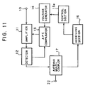
- Fig. 11 is a block diagram similar to Fig.1, and showing a fifth embodiment of the present invention.
- This embodiment takes advantage of the fact that a lower transmission level can be used when the receiving station is relatively close in range. This can be determined by detecting the field intensity level of a signal transmitted from the receiving station.
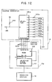
- the output signal of a detecting circuit of a received signal field intensity level provided in the receiving section 16 is introduced to a control section 15e, and as shown in Fig. 12, all the data signals of a ROM 153 are output from the control section 15e.
- a transmission output selection signal 152a which makes the transmission output level lower than the rated level within the tolerance range is output automatically to the voltage generator 14.
- Fig. 13B is a flow chart showing the operation of the control section 15e when the resistor 143a is selected as a resistor corresponding to a reference value.
- a transmission output selection signal 152a is output for selecting a resistor 143a so that the transmission output level becomes equal to a rated level.
- an address signal "0001” is output to make the output signal of the ROM 153 be "0000” (step ST11).
- an address signal "0101” is output to the ROM 153 (step ST13).
- the ROM 153 outputs the data "0011” and the selector 141a selects the resistor 143d.
- the transmission output level is lowered in the tolerance range.
- a detecting circuit for detecting received signal field intensity level provided in the receiving section 16 and a comparator for comparing a reference value with a detected value in the control section 15e are utilized.
- the control section 15e can be implemented by a microprocessor as in the case of the second embodiment.
- a transmission output level of a radio transceiver according to the present invention can be made higher or lower than each of the reference levels within the tolerance range in each level by the level conversion designating means; thereby the power consumption of a transceiver can be lowered and the transmission output level can be raised when noise level is high.
Applications Claiming Priority (2)
| Application Number | Priority Date | Filing Date | Title |
|---|---|---|---|
| JP88105/89 | 1989-04-10 | ||
| JP1088105A JP2769478B2 (ja) | 1989-04-10 | 1989-04-10 | 無線機 |
Publications (3)
| Publication Number | Publication Date |
|---|---|
| EP0392079A2 EP0392079A2 (en) | 1990-10-17 |
| EP0392079A3 EP0392079A3 (en) | 1992-05-06 |
| EP0392079B1 true EP0392079B1 (en) | 1996-05-01 |
Family
ID=13933593
Family Applications (1)
| Application Number | Title | Priority Date | Filing Date |
|---|---|---|---|
| EP89120669A Expired - Lifetime EP0392079B1 (en) | 1989-04-10 | 1989-11-08 | Radio transceiver |
Country Status (5)
| Country | Link |
|---|---|
| US (1) | US5086508A (ja) |
| EP (1) | EP0392079B1 (ja) |
| JP (1) | JP2769478B2 (ja) |
| AU (1) | AU614438B2 (ja) |
| CA (1) | CA2002389C (ja) |
Families Citing this family (38)
| Publication number | Priority date | Publication date | Assignee | Title |
|---|---|---|---|---|
| JPH0775324B2 (ja) * | 1989-08-18 | 1995-08-09 | 日本電気株式会社 | 携帯無線機 |
| AT401827B (de) * | 1989-12-11 | 1996-12-27 | Oesterr Forsch Seibersdorf | Messsender sowie verfahren zum kalibrieren von messstrecken |
| CA2035203C (en) * | 1990-01-30 | 1995-02-14 | Tsuguo Hori | Signal control apparatus capable of readily changing an apparatus output signal |
| JPH07101852B2 (ja) * | 1990-06-08 | 1995-11-01 | 三菱電機株式会社 | 送信電力制御回路 |
| SE467386B (sv) * | 1990-10-05 | 1992-07-06 | Ericsson Telefon Ab L M | Foerfarande foer reglering av uteffekt i mobilradiosystem |
| US5631921A (en) * | 1990-11-16 | 1997-05-20 | Interdigital Technology Corp. | Adaptive power control for a spread spectrum communications system and method |
| US5535238A (en) | 1990-11-16 | 1996-07-09 | Interdigital Technology Corporation | Spread spectrum adaptive power control communications system and method |
| US6873643B2 (en) | 1990-11-16 | 2005-03-29 | Interdigital Technology Corporation | Spread spectrum adaptive power control communications system and method |
| US5093840A (en) * | 1990-11-16 | 1992-03-03 | Scs Mobilecom, Inc. | Adaptive power control for a spread spectrum transmitter |
| BR9106405A (pt) * | 1990-12-20 | 1993-05-04 | Motorola Inc | Circuidade de controle de energia,telefone celular de acesso multiplo de divisao de tempo |
| JP2871889B2 (ja) * | 1991-04-16 | 1999-03-17 | 三菱電機株式会社 | 高周波電力増幅装置 |
| US5335360A (en) * | 1991-06-25 | 1994-08-02 | Motorola, Inc. | Base site selection apparatus and method |
| GB2258370B (en) * | 1991-08-02 | 1995-09-06 | Technophone Ltd | Cellular telephone |
| FI91201C (fi) * | 1992-06-05 | 1994-05-25 | Nokia Mobile Phones Ltd | Boosteri |
| US5333175A (en) * | 1993-01-28 | 1994-07-26 | Bell Communications Research, Inc. | Method and apparatus for dynamic power control in TDMA portable radio systems |
| SE513813C2 (sv) * | 1993-02-05 | 2000-11-06 | Ericsson Ge Mobile Communicat | Anordning med SAW-filter för duplexöverföring |
| US5669066A (en) * | 1993-05-14 | 1997-09-16 | Telefonaktiebolaget Lm Ericsson | Dynamic control of transmitting power at a transmitter and attenuation at a receiver |
| JPH06326631A (ja) * | 1993-05-17 | 1994-11-25 | Sony Corp | 無線通信機 |
| CA2166984A1 (en) * | 1993-07-26 | 1995-02-02 | Steve Carter | Method and apparatus for controlling the exposure to rf transmissions |
| JP2974895B2 (ja) * | 1993-09-16 | 1999-11-10 | 富士通株式会社 | 携帯用無線装置 |
| FI108765B (fi) * | 1993-09-28 | 2002-03-15 | Nokia Corp | Menetelmä ja laitteisto solukkoradiojärjestelmän tukiaseman vastaanottimen vahvistusvirheen mittaamiseksi ja kentänvoimakkuusmittauksen tarkentamiseksi |
| US5471655A (en) * | 1993-12-03 | 1995-11-28 | Nokia Mobile Phones Ltd. | Method and apparatus for operating a radiotelephone in an extended stand-by mode of operation for conserving battery power |
| JP3158833B2 (ja) * | 1994-01-27 | 2001-04-23 | 三菱電機株式会社 | 移動無線装置 |
| US5761622A (en) * | 1995-05-18 | 1998-06-02 | Ericsson Inc. | Method and apparatus for controlling operation of a portable or mobile battery-operated radios |
| US5854972A (en) * | 1996-05-16 | 1998-12-29 | Motorola, Inc. | Circuit for adjusting transmit power |
| JP3254390B2 (ja) * | 1996-10-18 | 2002-02-04 | 三菱電機株式会社 | 送信電力制御装置 |
| JPH10215130A (ja) * | 1997-01-30 | 1998-08-11 | Mitsubishi Electric Corp | 増幅装置及び送信出力制御装置 |
| US5893036A (en) * | 1997-01-30 | 1999-04-06 | Motorola, Inc. | Transmission power control method |
| US5987333A (en) * | 1997-09-30 | 1999-11-16 | Nortel Networks Corporation/Corporation Nortel Networks | Communications power control |
| FR2813487B1 (fr) * | 2000-08-31 | 2002-11-29 | Cit Alcatel | Procede et dispositif de controle de l'amplification du signal emis par un terminal mobile permettant d'augmenter l'autonomie dudit terminal mobile |
| JP2004529904A (ja) * | 2001-03-14 | 2004-09-30 | ブリストル−マイヤーズ スクイブ カンパニー | 増殖性疾患の治療のためのエポシロン類似体および化学療法剤の組み合わせ |
| US20040203984A1 (en) * | 2002-06-11 | 2004-10-14 | Tai-Her Yang | Wireless information device with its transmission power lever adjustable |
| US6806767B2 (en) * | 2002-07-09 | 2004-10-19 | Anadigics, Inc. | Power amplifier with load switching circuit |
| DE60321392D1 (de) * | 2003-01-31 | 2008-07-10 | Nokia Corp | Ausgangsleistungsregelung für aufwärtsverbindungen mit mehreren zeitschlitzen |
| US7418032B2 (en) * | 2005-03-15 | 2008-08-26 | International Business Machines Corporation | Altering power consumption in communication links based on measured noise |
| US8125243B1 (en) * | 2007-03-12 | 2012-02-28 | Cypress Semiconductor Corporation | Integrity checking of configurable data of programmable device |
| US10240456B2 (en) * | 2013-03-15 | 2019-03-26 | Merlin Technology, Inc. | Inground device with advanced transmit power control and associated methods |
| US9425619B2 (en) | 2013-03-15 | 2016-08-23 | Merlin Technology, Inc. | Advanced inground device power control and associated methods |
Family Cites Families (14)
| Publication number | Priority date | Publication date | Assignee | Title |
|---|---|---|---|---|
| JPS6110327Y2 (ja) * | 1980-01-10 | 1986-04-03 | ||
| DE3312112A1 (de) * | 1983-04-02 | 1984-10-11 | ELNA GmbH, 2084 Rellingen | Sender- und empfaengeranlage fuer sprechfunk zwischen fahrzeugen auf see und auf dem rhein |
| US4523155A (en) * | 1983-05-04 | 1985-06-11 | Motorola, Inc. | Temperature compensated automatic output control circuitry for RF signal power amplifiers with wide dynamic range |
| JPS6060321A (ja) * | 1983-09-13 | 1985-04-06 | Nippon Seiko Kk | 旋回輪軸受 |
| US4613990A (en) * | 1984-06-25 | 1986-09-23 | At&T Bell Laboratories | Radiotelephone transmission power control |
| JPH0644716B2 (ja) * | 1984-08-14 | 1994-06-08 | 日本電気株式会社 | 無線通信装置 |
| JPS6261231A (ja) * | 1985-09-10 | 1987-03-17 | 株式会社東芝 | 回路しや断器 |
| JPS62286324A (ja) * | 1986-06-05 | 1987-12-12 | Nec Corp | 携帯用電話機 |
| JPS6333021A (ja) * | 1986-07-26 | 1988-02-12 | Nec Corp | 携帯無線電話機 |
| JPS6346824A (ja) * | 1986-08-14 | 1988-02-27 | Kokusai Denshin Denwa Co Ltd <Kdd> | 送信電力制御方式 |
| JPS63226124A (ja) * | 1986-10-29 | 1988-09-20 | Oki Electric Ind Co Ltd | 無線装置用レベル制御回路 |
| DE3710001A1 (de) * | 1987-03-26 | 1988-10-06 | Bosch Gmbh Robert | Schnurloses telefon |
| US4825193A (en) * | 1988-01-07 | 1989-04-25 | Motorola, Inc. | Acknowledge back pager with adaptive variable transmitter output power |
| JPH0728231B2 (ja) * | 1989-04-10 | 1995-03-29 | 三菱電機株式会社 | ブースタ装置およびブースタ装置を接続した無線機 |
-
1989
- 1989-04-10 JP JP1088105A patent/JP2769478B2/ja not_active Expired - Lifetime
- 1989-11-06 AU AU44462/89A patent/AU614438B2/en not_active Ceased
- 1989-11-07 CA CA002002389A patent/CA2002389C/en not_active Expired - Fee Related
- 1989-11-07 US US07/432,862 patent/US5086508A/en not_active Expired - Lifetime
- 1989-11-08 EP EP89120669A patent/EP0392079B1/en not_active Expired - Lifetime
Also Published As
| Publication number | Publication date |
|---|---|
| CA2002389A1 (en) | 1990-10-10 |
| EP0392079A3 (en) | 1992-05-06 |
| CA2002389C (en) | 1994-03-29 |
| JP2769478B2 (ja) | 1998-06-25 |
| JPH02268028A (ja) | 1990-11-01 |
| EP0392079A2 (en) | 1990-10-17 |
| AU614438B2 (en) | 1991-08-29 |
| AU4446289A (en) | 1990-10-11 |
| US5086508A (en) | 1992-02-04 |
Similar Documents
| Publication | Publication Date | Title |
|---|---|---|
| EP0392079B1 (en) | Radio transceiver | |
| US4870698A (en) | Output power control circuit for a mobile radio apparatus | |
| US5303395A (en) | Power control with a constant gain amplifier for portable radio transceivers | |
| EP0172704B1 (en) | Battery-powered radio communication apparatus capable of prolonging the communicable state thereof | |
| US5854972A (en) | Circuit for adjusting transmit power | |
| EP0960475B1 (en) | Power saving device for radio communication terminal | |
| US5999829A (en) | Circuit and method for controlling the power used by a portable radiotelephone | |
| US6301486B1 (en) | Radio telephone apparatus | |
| US5815821A (en) | Method and a device for conserving power in a battery powered transceiver | |
| EP0639890A1 (en) | Directional detector for power level control | |
| EP1440506A1 (en) | Rf power amplifier circuit | |
| EP0772292A2 (en) | RF power amplifiers | |
| US4155112A (en) | Power supply circuitry | |
| US6057732A (en) | Transmission power control circuit and method for CDMA system | |
| JPH09148958A (ja) | アンテナ及び無線装置 | |
| EP0388895B1 (en) | Variable transmission power type transmitter | |
| US4458209A (en) | Adaptive power control circuit | |
| JP3623731B2 (ja) | 移動無線端末装置 | |
| EP0460280B1 (en) | Transmitting power control circuit | |
| US5610525A (en) | Battery capacity detector | |
| US20040072548A1 (en) | Transmission circuit suitable for dual-mode mobile phone | |
| JPS6243608B2 (ja) | ||
| JPH0481898B2 (ja) | ||
| KR960000932B1 (ko) | 과열방지 출력레벨 제어회로 | |
| KR200291223Y1 (ko) | 기지국 송신기의 출력레벨 제어회로 |
Legal Events
| Date | Code | Title | Description |
|---|---|---|---|
| PUAI | Public reference made under article 153(3) epc to a published international application that has entered the european phase |
Free format text: ORIGINAL CODE: 0009012 |
|
| AK | Designated contracting states |
Kind code of ref document: A2 Designated state(s): FR GB SE |
|
| PUAL | Search report despatched |
Free format text: ORIGINAL CODE: 0009013 |
|
| AK | Designated contracting states |
Kind code of ref document: A3 Designated state(s): FR GB SE |
|
| 17P | Request for examination filed |
Effective date: 19920703 |
|
| 17Q | First examination report despatched |
Effective date: 19930803 |
|
| GRAH | Despatch of communication of intention to grant a patent |
Free format text: ORIGINAL CODE: EPIDOS IGRA |
|
| GRAA | (expected) grant |
Free format text: ORIGINAL CODE: 0009210 |
|
| AK | Designated contracting states |
Kind code of ref document: B1 Designated state(s): FR GB SE |
|
| ET | Fr: translation filed | ||
| PLBE | No opposition filed within time limit |
Free format text: ORIGINAL CODE: 0009261 |
|
| STAA | Information on the status of an ep patent application or granted ep patent |
Free format text: STATUS: NO OPPOSITION FILED WITHIN TIME LIMIT |
|
| 26N | No opposition filed | ||
| REG | Reference to a national code |
Ref country code: GB Ref legal event code: IF02 |
|
| REG | Reference to a national code |
Ref country code: GB Ref legal event code: 746 Effective date: 20020306 |
|
| REG | Reference to a national code |
Ref country code: FR Ref legal event code: D6 |
|
| PGFP | Annual fee paid to national office [announced via postgrant information from national office to epo] |
Ref country code: GB Payment date: 20051102 Year of fee payment: 17 |
|
| PGFP | Annual fee paid to national office [announced via postgrant information from national office to epo] |
Ref country code: SE Payment date: 20051107 Year of fee payment: 17 |
|
| PGFP | Annual fee paid to national office [announced via postgrant information from national office to epo] |
Ref country code: FR Payment date: 20051108 Year of fee payment: 17 |
|
| PG25 | Lapsed in a contracting state [announced via postgrant information from national office to epo] |
Ref country code: SE Free format text: LAPSE BECAUSE OF NON-PAYMENT OF DUE FEES Effective date: 20061109 |
|
| EUG | Se: european patent has lapsed | ||
| GBPC | Gb: european patent ceased through non-payment of renewal fee |
Effective date: 20061108 |
|
| REG | Reference to a national code |
Ref country code: FR Ref legal event code: ST Effective date: 20070731 |
|
| PG25 | Lapsed in a contracting state [announced via postgrant information from national office to epo] |
Ref country code: GB Free format text: LAPSE BECAUSE OF NON-PAYMENT OF DUE FEES Effective date: 20061108 |
|
| PG25 | Lapsed in a contracting state [announced via postgrant information from national office to epo] |
Ref country code: FR Free format text: LAPSE BECAUSE OF NON-PAYMENT OF DUE FEES Effective date: 20061130 |