EP0391690B1 - Bildaufnahmeeinrichtung mit elektronischer Bildvergrösserung - Google Patents
Bildaufnahmeeinrichtung mit elektronischer Bildvergrösserung Download PDFInfo
- Publication number
- EP0391690B1 EP0391690B1 EP90303618A EP90303618A EP0391690B1 EP 0391690 B1 EP0391690 B1 EP 0391690B1 EP 90303618 A EP90303618 A EP 90303618A EP 90303618 A EP90303618 A EP 90303618A EP 0391690 B1 EP0391690 B1 EP 0391690B1
- Authority
- EP
- European Patent Office
- Prior art keywords
- image pickup
- signals
- output
- delay
- color
- Prior art date
- Legal status (The legal status is an assumption and is not a legal conclusion. Google has not performed a legal analysis and makes no representation as to the accuracy of the status listed.)
- Expired - Lifetime
Links
Images


Classifications
-
- H—ELECTRICITY
- H04—ELECTRIC COMMUNICATION TECHNIQUE
- H04N—PICTORIAL COMMUNICATION, e.g. TELEVISION
- H04N5/00—Details of television systems
- H04N5/222—Studio circuitry; Studio devices; Studio equipment
- H04N5/262—Studio circuits, e.g. for mixing, switching-over, change of character of image, other special effects ; Cameras specially adapted for the electronic generation of special effects
- H04N5/2628—Alteration of picture size, shape, position or orientation, e.g. zooming, rotation, rolling, perspective, translation
-
- H—ELECTRICITY
- H04—ELECTRIC COMMUNICATION TECHNIQUE
- H04N—PICTORIAL COMMUNICATION, e.g. TELEVISION
- H04N5/00—Details of television systems
- H04N5/14—Picture signal circuitry for video frequency region
- H04N5/142—Edging; Contouring
-
- H—ELECTRICITY
- H04—ELECTRIC COMMUNICATION TECHNIQUE
- H04N—PICTORIAL COMMUNICATION, e.g. TELEVISION
- H04N5/00—Details of television systems
- H04N5/14—Picture signal circuitry for video frequency region
- H04N5/20—Circuitry for controlling amplitude response
- H04N5/205—Circuitry for controlling amplitude response for correcting amplitude versus frequency characteristic
- H04N5/208—Circuitry for controlling amplitude response for correcting amplitude versus frequency characteristic for compensating for attenuation of high frequency components, e.g. crispening, aperture distortion correction
-
- H—ELECTRICITY
- H04—ELECTRIC COMMUNICATION TECHNIQUE
- H04N—PICTORIAL COMMUNICATION, e.g. TELEVISION
- H04N7/00—Television systems
- H04N7/01—Conversion of standards, e.g. involving analogue television standards or digital television standards processed at pixel level
- H04N7/0135—Conversion of standards, e.g. involving analogue television standards or digital television standards processed at pixel level involving interpolation processes
Definitions
- the present invention generally relates to image pickup devices capable of picking up images while electronically enlarging the same. More particularly, the present invention relates to an image pickup device capable of picking up images while electronically enlarging the same which comprises a CCD image sensor as an image pickup element and is used, for example, in a video camera or a video tape recorder with a built-in camera.
- Fig. 23 is a schematic block diagram showing a conventional image pickup device capable of picking up images while electronically enlarging the same twice.
- a timing pulse generating circuit 109 generates a timing pulse for driving a CCD image sensor 101, a signal for controlling an analog switch 104, and several other pulses required for a signal processing circuit 106, in synchronization with synchronizing signals generated from a synchronizing signal generator 110.
- a switch SW1 for switching between the normal image pickup and the enlarged image pickup is connected to the timing pulse generating circuit 109.
- the timing pulse generating circuit 109 changes periods of a horizontal transfer pulse and a vertical transfer pulse according to operation of the switch SW1.
- the horizontal transfer pulse generated from the timing pulse generating circuit 109 is applied to the CCD image sensor 101 through a horizontal driver 111 and the vertical transfer pulse is applied to the CCD image sensor 101 through a vertical driver 112.
- Video signals outputted from the CCD image sensor 101 are applied to a sample and hold (S/H) circuit 102 to be sampled and held, and then applied to a 1H delay circuit 103 and the analog switch 104.
- the 1H delay circuit 103 delays the video signals 1H (one horizontal scanning period) for application to the analog switch 104.
- the analog switch 104 is responsive to a switching signal from the timing pulse generating circuit 109 for selecting output of either the sample and hold circuit 102 or the 1H delay circuit 103 and applying the selected one to the signal processing circuit 106.
- the signal processing circuit 106 comprises sample and hold circuits, processing circuits and an encoder for converting the video signals from the analog switch 104 into primary color signals R, G and B.
- the timing pulse generating circuit 109 applies the horizontal and vertical transfer pulses that have frequencies half those in the normal image pickup to the CCD image sensor 101 through the horizontal driver 111 and the vertical driver 112, respectively. Since frequencies of the horizontal and vertical transfer pulses become 1/2 with respect to those in the normal image pickup, it takes a twice time, or 2H to output charges of one horizontal line in the CCD image sensor 101. Charges corresponding to 1H of the 2H are unnecessary, so that they are replaced by required signals of 1H before that have been delayed by the 1H delay circuit 103. This replacement is effected by the analog switch 104. The unnecessary charges in the vertical direction (corresponding to a 1/2 area of a standard screen) are deleted by fast vertical transfer performed during a vertical blanking period so that they are not outputted as the video signals from the CCD image sensor 101.
- the 1H delay circuit 103 may be implemented, for example, as a CCD 1H delay circuit. Since the video signals entered in the signal processing circuit 106 have not yet undergone any processing, however, the signal processing circuit 106 will exhibit a very large dynamic range. On the other hand, such a delay circuit 103 as 1H constituted of a CCD or the like does not have a large dynamic range. Therefore, the use of such an element is impossible and thus miniaturization of the circuit can not be achieved. Additionally, in the conventional image pickup device shown in Fig. 23, a complementary color filter employed in the CCD image sensor 101 is limited to a vertical stripe filter only, so that a diced filter is unacceptable.
- Fig. 24 is a schematic block diagram showing part of a conventional image pickup device for the normal image pickup in which a diced filter is used as the complementary color filter
- Fig. 25 is a diagram showing relationship between line sequential color-difference signals C OH and 1H-delayed C 1H , an R channel component (R-Y) and a B channel component (B-Y).
- video signals outputted from a sample and hold circuit 102 are applied to an OB clamp circuit 108 where their optical black level is clamped, and then applied to sample and hold circuits 113 and 114.
- the sample and hold circuits 113 and 114 separate color components from the video signals to apply them to a signal processing circuit 115.
- a processed line sequential color-difference signal C OH is applied to a 1H delay circuit 116 and an analog switch 117.
- the 1H delay circuit 116 delays the line sequential color-difference signal C OH by 1H to obtain a C 1H which is applied to the analog switch 117.
- the analog switch 117 outputs an R channel component (R-Y) and a B channel component (B-Y) out of the line sequential color-difference signals C OH and C 1H .
- the CCD image sensor 101 which has a diced filter employed therein outputs a color-difference signal for every 1H line-sequentially.
- the 1H delay circuit 116 and the analog switch 117 are used.
- the relationship between the line sequential color-difference signals C OH and C 1H , the R channel component (R-Y) and the B channel component (B-Y) in this case will be as shown in Fig. 25.
- Fig. 26 is a block diagram of the image pickup device shown in Fig. 24 with an additional enlarging image pickup function
- Fig. 27 is a diagram showing relationship between the line sequential color-difference signals C OH , C 1H and C 2H , the R channel component (R-Y) and the B channel component (B-Y) in the image pickup device shown in Fig. 26.
- a 1H delay circuit 103 and an analog switch 104 between an OB clamp circuit 108 and sample and hold circuits 113 and 114, there are connected a 1H delay circuit 103 and an analog switch 104, and between a 1H delay circuit 116 and an analog switch 117, there are connected a 1H delay circuit 118 and an analog switch 119.
- the 1H delay circuit 103 and the analog switch 104 are provided for replacing unnecessary charges of 1H by required signals of 1H before in the enlarged image pickup through the same operation as in Fig. 23.
- the 1H delay circuit 118 and the analog switch 119 are provided to interpolate the color-difference signals in the enlarged image pickup.
- the image pickup device shown in Fig. 26 allows the enlarging image pickup as well as the normal image pickup even when a complementary color diced filter is used therein. As will be apparent from Fig. 26, however, provision of three 1H delay circuits is required. Further, for a luminance signal, there appear the same signal over two lines in the vertical direction, and for the color-difference signal, there appear the same signal over four lines. This produces indentation of a diagonal line or a curb and thus a mosaic picture, considerably deteriorating the picture quality.
- the same vertical and horizontal aperture circuits are used in the normal and enlarging image pickups. Since in the enlarging image pickup, however, the same signal appears over two lines in the vertical direction, good contour correction can not be made if the same vertical aperture circuit as in the normal image pickup is used. Further, since in the enlarging image pickup, the horizontal transfer pulse of the CCD image sensor 101 has a 1/2 frequency relative to that in the normal image pickup, signal band becomes 1/2. Therefore, again good contour correction can not be made if the same horizontal aperture circuit as in the normal image pickup is used. Additionally, if the same mix amount of aperture is used in the enlarging and the normal image pickups, there arises a problem that proper mix amount can not be provided for each case.
- An object of the present invention is to provide an image pickup device capable of picking up electronically enlarged images which is provided with delay means adapted only with provision of n/2 delay devices to delay a luminance signal or a color-difference signal by n horizontal scanning periods and to interpolate the same.
- Another object of the present invention is to provide an image pickup device capable of picking up electronically enlarged images which can improve picture quality in the enlarging image pickup by interpolating a luminance signal and a color-difference signal with the use of a said delay means.
- a preferred embodiment of the present invention provides an image pickup device capable of picking up electronically enlarged images which can produce horizontal and vertical aperture signals in the enlarging image pickup, based on luminance signals delayed by a said delay means.
- a preferred embodiment of the present invention provides an image pickup device capable of picking up electronically expanded images which can eliminate random noises contained in color-difference signals in the normal and the enlarging image pickups by making use of color-difference signals delayed by a said delay means.
- the invention provides an image pickup device capable of picking up images of an object while electronically enlarging the same twofold relative to those in the normal image pickup, said device including image pickup means for picking up images of said object to output video signals, characterised by: delay means for delaying said video signals by n horizontal scanning periods, said delay means having n/2 delay devices connected in series which sequentially delay the video signals by 0 to n horizontal scanning periods and individually output the delayed video signals; and interpolating means for forming line-interpolated output signals from said delayed video signals in the enlarging image pickup; each of said delay devices comprising: switching means for being switched to a first input to output said video signals in the normal image pickup and for being switched to the first input and to a second input alternately every one horizontal scanning period to output the video signals in the enlarging image pickup; a delay circuit for delaying output of said switching means by one horizontal scanning period; and gain control means for controlling gain of the output of said delay circuit and applying the output to the second input of said switching means.
- the invention provides an image pickup device capable of picking up images of an object while electronically enlarging the same twofold relative to those in the normal image pickup, said device including image pickup means (71) for picking up images of said object to output luminance signals, characterised by: a said delay means for delaying said luminance signals by n horizontal scanning periods, said delay means having n/2 delay devices connected in series which sequentially delay the luminance signals by 0 to n horizontal scanning periods and individually output the delayed luminance signals; luminance signal interpolating means for outputting interpolated luminance signals by effecting switching between a signal obtained by operating on the luminance signals that have been delayed by 0, 2, 4 and 6 horizontal scanning periods and outputted from said delay means and the luminance signal that has been delayed by 3 horizontal scanning periods; and first selecting means for selecting said output luminance signals in the normal image pickup and said output interpolated luminance signals in the enlarging image pickup.
- image pickup means (71) for picking up images of said object to output luminance signals, characterised by: a said delay means for delaying said luminance
- the invention provides an image pickup device capable of picking up images of an object while electronically enlarging the same twofold relative to those in the normal image pickup, said device including a solid-state image pickup element with color filters arranged therein in diced complementary color mosaic structure, characterised by: a said delay means for delaying color-difference signals outputted from said solid-state image pickup element by n horizontal scanning periods, said delay means having n/2 delay devices connected in series which sequentially delay the color-difference signals by 0 to n horizontal scanning periods and individually output the delayed color-difference signals; and color difference signal interpolating means for outputting interpolated color-difference signals by operating to form combinations of the color-difference signals individually delayed and outputted from said delay means (142) and effecting switching between the respective operation outputs for every one horizontal scanning period.
- the invention provides a method of electronically enlarging a video image, characterised by the steps of: delaying color-difference or luminance signals by operating a delay means comprising n/2 delay devices connected in series, each device having one delay circuit providing a delay corresponding to one horizontal scanning period, to produce respective signals delayed by 0 to n horizontal scanning periods; and selectively combining said delayed signals to form line-interpolated signals representing the enlarged video image.
- delay means which has n/2 delay devices connected in series therein and outputs signals delayed by the delay devices by 0 to n scanning periods, luminance signals or color-difference signals can be delayed by n horizontal scanning periods, and this means that reduction of the delay circuits in number is possible. Therefore, even if the delay circuits are implemented as CCD 1H delay units, the cost can be kept low.
- switching is effected between those luminance signals delayed by said delay means by 0, 2, 4 and 6 horizontal scanning periods and the luminance signal delayed by the same by 3 horizontal scanning periods for every one horizontal scanning period to output a luminance interpolating signal.
- the luminance signals can be interpolated by use of the delay means, so that picture quality can be improved in the enlarging image pickup.
- a carrier component and a higher harmonic component contained in the luminance signal in the normal image pickup are eliminated by a first filter and the carrier component and a higher harmonic component contained in the luminance signal in the enlarging image pickup are eliminated by a second filter. Accordingly, in the normal image pickup, output of the first filter is selected and that of the second filter is selected in the enlarged image pickup.
- the carrier component and the higher harmonic component contained in the luminance signal in both the normal and the enlarging image pickups are eliminated, so that the picture quality can be improved.
- vertical contour correction of an image is made by operating the luminance signals delayed by predetermined horizontal scanning periods and outputted from the delay means.
- a proper picture quality can be obtained through the vertical contour correction of an image.
- the luminance signals are delayed for production of horizontal contour correcting signals in the normal and the enlarging image pickups and the delayed outputs are selected to produce horizontal aperture signals most suitable for the normal and the enlarging image pickups, respectively, so that the picture quality can be improved.
- the horizontal aperture signal, the vertical aperture signal and the luminance signal are added together and switched to have their respective optimum levels for making contour correction of an image.
- an image pickup device capable of picking up images of an object while electronically enlarging the same twice relative to the normal image pickup, which comprises a solid-state image pickup element having color filters arranged in diced complementary mosaic structure therein, a combination of the color-difference signals delayed by 0 to n horizontal scanning periods and outputted from the delay means are operated, and switching is effected between the respective operation outputs for every one horizontal scanning period to output interpolated color-difference signals.
- the color-difference signals are interpolated by use of the delay means, so that the picture quality can be improved in the enlarging image pickup as well as in the normal image pickup.
- color-difference signals delayed by 2 horizontal scanning periods and outputted in the normal image pickup or color-difference signals delayed by 4 horizontal scanning periods and outputted in the enlarged image pickup and undelayed color-difference signals are operated together to suppress noises contained in the color-difference signals, so that the picture quality can be improved.
- the carrier component and the higher harmonic component contained in the color-difference signal are eliminated, so that the attenuation of the carrier and the higher harmonic components contained in the color-difference signal allows improvement in the picture quality.
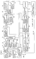
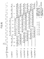
- Fig. 1 is a schematic block diagram showing the entire structure of an embodiment of the present invention.
- Fig. 2 is block diagram showing a specific example of the low-pass filter for luminance signals shown in Fig. 1.
- Fig. 3 is a schematic block diagram of a 6H delay circuit.
- Fig. 4 is a specific block diagram of a 1H delay unit constituting a 6H delay circuit.
- Fig. 5 is a typical waveform chart of the luminance signals each delayed by the 6H delay circuit which is employed for interpolating the luminance signals.
- Fig. 6 is a specific block diagram of a luminance signal interpolating circuit.
- Fig. 7 is a waveform chart for explaining operation of the luminance signal interpolating circuit.
- Fig. 8 is a specific block diagram of a luminance signal switching circuit.
- Fig. 9 is a block diagram showing a specific example of a vertical aperture circuit.
- Fig. 10 is a waveform chart for explaining operation of the vertical aperture circuit.
- Fig. 11 is a waveform chart for explaining operation of the vertical aperture circuit in the normal image pickup.
- Fig. 12 is a block diagram showing a specific example of a horizontal aperture circuit and an aperture adding circuit.
- Fig. 13 is a waveform chart for explaining operation of the horizontal aperture circuit.
- Fig. 14 is a block diagram showing a specific example of a low-pass filter for color-difference signals.
- Fig. 15 is a typical waveform chart of the color-difference signals sequentially delayed by the 6H delay circuit.
- Fig. 16 is a block diagram showing a specific example of a color-difference signal interpolating circuit.
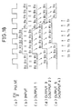
- Fig. 17 is a diagram showing color-difference signal interpolating methods in the enlarging image pickup in a table.
- Fig. 18 is a typical waveform chart of the color-difference signals outputted from the 6H delay circuit in the normal image pickup.
- Fig. 19 is a diagram showing output of the color-difference interpolating circuit for every 1H during the timings T0 to T7.
- Fig. 20 is block diagram showing a color-difference signal switching circuit.
- Fig. 21 is a block diagram showing a specific example of a CNR circuit.
- Fig. 22 is a waveform chart of the respective parts of the CNR circuit for explaining operation thereof.
- Fig. 23 is a schematic block diagram of a conventional image pickup device capable of the enlarging image pickup.
- Fig. 24 is a schematic block diagram showing a conventional image pickup device for the normal image pickup where a diced filter is used as a complementary color filter.
- Fig. 25 is a diagram showing line-sequential color-difference signals and R and B channel components of Fig. 24 in a table.
- Fig. 26 is a block diagram showing the image pickup device shown in Fig. 24 with an additional enlarging image pickup function.
- Fig. 27 is a diagram showing the line-sequential color-difference signals and the R and the B channel components of Fig. 26 in a table.
- Fig. 1 is a schematic block diagram showing the entire structure of an embodiment of the present invention. Referring to the diagram, the entire structure of an embodiment of the present invention will be described.
- a timing pulse generating circuit 74 is provided to generate several timing pulses for driving a CCD image sensor 71.
- the timing pulse generating circuit 74 receives a horizontal drive pulse HD and a vertical drive pulse VD from a synchronizing signal generator 77. Further, a switch SW1 for switching between the normal image pickup and the enlarging image pickup is connected to the timing pulse generating circuit 74.
- a horizontal transfer pulse generated from the timing pulse generating circuit 74 is applied to the CCD image sensor 71 through a horizontal driver 81 while a vertical transfer pulse is applied to the CCD image sensor 71 through a vertical driver 82.
- An output signal of the CCD image sensor 71 is applied to a sample and hold circuit 72 to be sampled and held in response to a sampling pulse applied thereto from the timing pulse generating circuit 74.
- the sampled and held video signal is applied to an OB clamp circuit 73.
- the OB clamp circuit 73 clamps an optical black portion located in the last portion of a horizontal picture element in response to an optical black clamp pulse applied from the timing pulse generating circuit 74 so as to define reference black level (pedestal level) for signal processing.
- Output of the OB clamp circuit 73 is applied to a processing circuit 75 and sample and hold circuits 76a and 76b.
- the sample and hold circuits 76a and 76b are responsive to a sampling pulse from the timing pulse generating circuit 74 for separating color signals and applying the thus separated color signals to the processing circuit 75.
- the processing circuit 75 is provided to perform signal processings such as AGC, ⁇ correction, white balance, KNEE and ALC.
- the processing circuit 75 outputs a color-difference signal and a luminance signal and the latter signal is applied to a low-pass filter 58 for luminance signals.
- the low-pass filter 58 for luminance signals is provided to attenuate a carrier component and a higher harmonic component contained in the luminance signal, corresponding to different frequencies of the horizontal transfer pulses in the normal and the enlarging image pickups, respectively.
- the luminance signals in the normal image pickup are applied to a luminance signal switching circuit 24 while they are applied to a 6H delay circuit 141 in the enlarging image pickup.
- the 6H delay circuit 141 sequentially delays the luminance signals by 0H to 6H periods for output.
- the delayed luminance signals outputted from the 6H delay circuit 141 are applied to a luminance signal interpolating circuit 20.
- the luminance signal interpolating circuit 20 is responsive to the delayed luminance signals for outputting and applying interpolated luminance signals to the luminance signal switching circuit 24.
- the luminance signal switching circuit 24 selects the luminance signals outputted from the low-pass, filter 58 for luminance signals in the normal image pickup and in the enlarged image pickup, selects the luminance signals having been interpolated by the luminance signal interpolating circuit 20 to apply them to a horizontal aperture circuit 64.
- the horizontal aperture circuit 64 produces horizontal aperture signals corresponding to different frequencies of the horizontal transfer pulses and thus to different frequency characteristics of the video signals in the normal and the enlarging image pickups, respectively, and applies them to an aperture adding circuit 70.
- the luminance signals delayed in the 6H delay circuit 141 are also applied to a vertical aperture circuit 36 which produces vertical aperture signals corresponding to the normal and the enlarging image pickups, respectively, and applies them to the aperture adding circuit 70.
- the aperture adding circuit 70 is provided to change addition amount of aperture depending on the normal image pickup or the enlarging image pickup, since characteristics of the vertical and the horizontal aperture signals and further of the luminance signals before passing through the respective aperture circuits in the normal image pickup mode differ from those in the enlarging image pickup mode.
- the color-difference signals outputted from the processing circuit 75 are applied to another low-pass filter 52 for color-difference signals.
- the low-pass filter 52 for color-difference signals is provided to attenuate a carrier component and a higher harmonic component contained in the color-difference signals and is switched corresponding to the normal and the enlarging image pickups, respectively, since frequency difference of the horizontal transfer pulse is seen therebetween.
- the color-difference signals outputted from the low-pass filter 52 for color-difference signals are applied to a CNR circuit 47.
- the CNR circuit 47 is provided to suppress random noises contained in the color-difference signals and receive color-difference signals sequentially delayed by 2H or 4H and outputted from a following 6H delay circuit 142.
- the color-difference signals having had the random noises suppressed by the CNR circuit 47 are applied to the 6H delay circuit 142.
- the 6H delay circuit 142 sequentially delays the color-difference signals by 0H to 6H and applies the delayed ones to a color-difference signal interpolating circuit 30.
- the color-differnece signal interpolating circuit 30 is responsive to the color-difference signals having been delayed by 0H to 6H for applying interpolated color-difference signals to a color-difference signal converting circuit 31.
- the color-difference signal converting circuit 31 converts the interpolated color-difference signals into R-Y signals and B-Y signals and outputs the converted signals to an encoder 78 through the processing circuit 75.
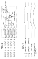
- Fig. 2 is a specific block diagram of a low-pass filter for luminance signals.
- a low-pass filter 58 for luminance signals is provided to switch a low-pass filter with a trap which attenuates the carrier component and the higher harmonic component contained in the luminance signals, since in the enlarging image pickup, frequency of the horizontal transfer pulse becomes 1/2 of that in the normal image pickup.
- the low-pass filter 58 for luminance signals comprises buffers 531, 532, and 533, low-pass filters 54 and 55, a wide-band CCD 1H delay circuit 56 and a low-pass filter 57, as shown in Fig. 2.
- Luminance signals are applied to the low-pass filters 54 and 55 through the buffer 531.
- the low-pass filter 54 is one with a trap for the normal image pickup and the low-pass filter 55 is one with a trap for the enlarging image pickup.
- Output of the low-pass filter 54 is applied to the wide-band CCD 1H delay circuit 56 where it is delayed by 1H so as to correspond to delay time of the color-difference signals.
- the luminance signals delayed in the wide-band CCD 1H delay circuit 56 are outputted through the low-pass filter 57 with a trap for attenuating the clock and the higher harmonic components, and through the buffer 533 to be further applied to the luminance signal switching circuit 24 shown in Fig. 1.
- Output of the low-pass filter 55 is applied to a 6H delay circuit 141 through the buffer 532.
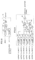
- Fig. 3 is a block diagram showing the entire structure of a 6H delay circuit and Fig. 4 is a specific block diagram of a 1H delay unit constituting the 6H delay circuit.
- the 6H delay circuit 141 comprises three 1H delay units 131, 132 and 133 each of which comprises outputs A and B. Each output B is connected to the 1H delay unit in the subsequent stage, so that the three 1H delay units 131, 132 and 133 are connected to each other in series.
- Each of the 1H delay units 131, 132 and 133 comprises clamp circuits 81 and 82, an analog switch 9, a CCD 1H delay circuit 10, a low-pass filter 11, a voltage control amplifier (VCA) 12 and a buffer 201, as shown in Fig. 4.
- Luminance signals are applied to the clamp circuit 81.
- the clamp circuit 81 is provided to fix the black level of the signals to be entered in the analog switch 9 at reference voltage V CP . Without this clamp circuit 81, there appears difference in the black level of outputs at a common output terminal of the analog switch 9 between one 1H and another, and this equivalently increases input amplitude of the CCD 1H delay circuit 10, resulting in a reduction in the dynamic range.
- the clamp circuit 82 is provided also for the same reason and clamps output of the VCA 12.
- Outputs of the clamp circuits 81 and 82 are applied to the analog switch 9.
- the analog switch 9 is switched by an ET ⁇ F H /2 pulse outputted from the timing pulse generating circuit 74 shown in Fig. 1.
- the analog switch 9 selects input 0, or output of the clamp circuit 81.
- the analog switch 9 selects input 0, or output of the clamp circuit 81 and when the same attains the "H" level, it selects input 1, or output of the clamp circuit 82 for every 1H.
- the common terminal output of the analog switch 9 is outputted through the buffer 201 as output A and at the same time, applied to the CCD 1H delay circuit 10.
- the CCD 1H delay circuit 10 is provided to delay the common terminal output of the analog switch 9 by 1H, output of which is applied to the low-pass filter 11.
- the low-pass filter 11 is provided to attenuate a clock signal F CK component and a higher harmonic component applied to the CCD 1H delay circuit 10.
- Output of the low-pass filter 11 is applied to the VCA 12.
- the VCA 12 changes gain according to a gain control signal so that the output B may have an amplitude equal to that of the input signal. In this manner, with the use of the clamp circuits 81 and 82 and the VCA 12, outputs that are consistent in the black level and amplitude from 1H to another can be obtained at the outputs A and B.
- the 6H delay circuit In the enlarging image pickup, an effective component and an ineffective component of the luminance signal are alternately outputted, one for every 1H.
- the analog switch 9 When the ET ⁇ F H /2 pulse which is a 2H period pulse, or inverted between the "H" level and the "L" level for every 1H is applied in the enlarging image pickup, the analog switch 9 outputs an input signal as it is for the output A when the ET ⁇ F H /2 is at the "L" level, and outputs a signal which has been outputted just 1H before at the output A for the output B.
- a control terminal of the analog switch 9 is fixed at the "L" level, so that an input signal of the 1H delay unit 13 is outputted as it is at the output A and another input signal which has preceded the former by 1H is outputted at the output B.
- Fig 5 is a timing chart showing the delayed luminance signals outputted from the 6H delay circuit.
- the luminance signal outputted from the low-pass filter 58 for luminance signals in the enlarging image pickup includes effective components (shown by 0 through 11) and ineffective components (shown by x), as shown in Fig. 5 (b).
- effective components shown by 0 through 11
- ineffective components shown by x
- a signal “0” delayed by 1H with respect to the output 1 is outputted to the output 2 of the 6H delay circuit 141 while the signal “0” is also outputted to the output 1 through the analog switch 9. Further, this "0" signal is delayed by 1H and outputted to the output 2. Therefore, the signal “0” is outputted to the output 2 after 2H from the first output of the signal "0” at the output 1, so that 0H (an undelayed signal) and 2H (a signal delayed by 2H) appear at the outputs 1 and 2 at a time (only if the ET ⁇ F H /2 pulse is at the "L" level).
- a single 1H delay unit can be used as a 2H delay circuit. Therefore, as shown in Fig. 3, a 6H delay circuit can be constituted by connecting three 1H delay units 131, 132 and 133 in series, so that a considerable reduction in costs can be achieved as compared with a case where as many as six relatively expensive CCD 1H delay units are simply connected to each other.
- This 6H delay circuit 141 is connected to the luminance signal interpolating circuit 20 which outputs interpolated luminance signals, as will be described in the following.
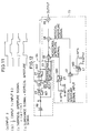
- Fig. 6 is a specific block diagram showing a luminance signal interpolating circuit.
- the luminance signal interpolating circuit 20 comprises four clamp circuits 151, 152, 153 and 154, which receive the output signals 1, 3, 5 and 6 of the 6H delay circuit 141 as input signals 1, 2, 3 and 4, respectively.
- Outputs of the clamp circuits 151 and 154 are applied to an adding and averaging circuit 161 where they are added together and averaged before being further applied to one input terminal of an operational amplifier 17.
- Outputs of the clamp circuits 152 and 153 are applied to another adding and averaging circuit 152 where also an addition average thereof is produced to be further applied to the other input terminal of the operational amplifier 17.
- the output of the clamp circuit 152 is also applied to a VCA 18 which is responsive to a gain control signal for controlling gain.
- Outputs of the operational amplifier 17 and the VCA 18 are applied to an analog switch 19.
- the analog switch 19 selects the output of the operational amplifier 17 when the ET ⁇ F H /2 pulse turns to the "L" level and selects the output of the VCA 18 when the same attains the "H" level to output an interpolated luminance signal.
- Fig. 7 is a timing chart for explaining operation of the luminance signal interpolating circuit 20 shown in Fig. 6. Referring to this chart, operation of the luminance signal interpolating circuit 20 shown in Fig. 6 will be described.
- the adding and averaging circuit 161 adds and averages the input signals 1 and 4 which have been clamped by the clamp circuits 151 and 154, as shown in Fig. 7 (b).
- the other adding and averaging circuit 162 adds and averages the input signals 2 and 3 which have been clamped by the clamp circuits 152 and 153, as shown in Fig. 7 (a).
- the operational amplifier 17 increases output of the adding and averaging circuit 162 by ⁇ times and that of the adding and averaging circuit 161 by ⁇ times to output such a signal as shown in Fig. 7 (c). Further, the input signal 2 having been clamped by the clamp circuit 152 is controlled by the VCA 18 for its gain.
- the analog switch 19 selects either output of the operational amplifier 17 or that of the VCA 18 for every 1H to output an interpolated luminance signal as shown in Fig. 7 (d).
- an interpolating signal is produced based on adjacent two sets of two sequential effective signals, or four effective signals in total. Therefore, when cubic curve interpolation is made, ⁇ ⁇ 1.12 and ⁇ ⁇ 0.12 are selected. Meanwhile, when all the four effective components have the same waveform, or vertical correlation is found therebetween, gain of the VCA 18 is adjusted so that the interpolating signal and the input signal 2 have the same waveform, whereby amplitude difference in the interpolated outputs between one 1H and another will be eliminated.
- Fig. 8 is a specific block diagram of a luminance signal switching circuit. Referring to the diagram, a luminance signal switching circuit 24 will be described. Luminance signals outputted from the low-pass filter 58 for luminance signals in the normal image pickup are applied to one input terminal of an analog switch 22 through a clamp circuit 211. The luminance signals that have been interpolated by the luminance signal interpolating circuit 20 are applied to the other input terminal of the analog switch 22 through another clamp circuit 212.
- a select signal ET turns to the "L" level in the normal image pickup
- the analog switch 22 selects output of the clamp circuit 211 to apply the same to the horizontal aperture circuit 64 shown in Fig. 1 through a buffer 23.
- the select signal ET attains the "H" level in the enlarging image pickup, the analog switch 22 outputs an interpolated luminance signal which is applied through the clamp circuit 212.
- Fig. 9 is a specific block diagram of a vertical aperture circuit.
- a luminance signal which has been delayed by the 6H delay circuit 141 in the enlarging image pickup will be as shown in Fig. 5, resulting in the interpolated output shown in Fig. 7 (d) after passing through the luminance signal interpolating circuit shown in Fig. 6. Since this interpolated output is a smooth one with its folded distortion in a high range (for example, indentation of a diagonal line) attenuated, a vertical aperture circuit 36 as shown in Fig. 9 is required.
- the vertical aperture circuit 36 comprises clamp circuits 321 to 326 for receiving the output signals 1 to 6 of the luminance signals delayed by the 6H delay circuit 141, adding and averaging circuits 331 to 334, analog switches 341 and 342 and an operational amplifier 35.
- the clamp circuits 321 to 326 receive the output signals 1 to 6 of the luminance signals delayed by the 6H delay circuit 141 as input signals 1 to 6, respectively, and clamp the received signals.
- the adding and averaging circuit 331 adds and averages the input signals 3 and 4 that have been clamped in the clamp circuits 323 and 324 to apply such a signal as shown in Fig. 10 (a) to 1 input terminal of the analog switch 341, while 0 input terminal of the same receives the input 3 which has been clamped in the clamp circuit 323.
- the adding and averaging circuit 332 adds and averages the input signals 1 and 5 that have been clamped in the clamp circuits 321 and 325 to apply such a signal as shown in Fig. 10 (b) to the adding and averaging circuit 334 and 0 input terminal of the analog switch 342.
- the adding and averaging circuit 333 adds and averages the input signals 2 and 6 that have been clamped in the clamp circuits 322 and 326 to apply such a signal as shown in Fig. 10 (c) to the adding and averaging circuit 334.
- the adding and averaging circuit 334 adds and averages outputs of the adding and averaging circuit 332 and 333 to apply the resultant signal as shown in Fig. 10 (d) to 1 input terminal of the analog switch 342.
- the analog switches 341 and 342 are set to the side of the 0 input terminals when a select signal ET turns to the "L" level in the normal image pickup, and set to the side of the 1 input terminals when the same attains the "H" level in the enlarging image pickup.
- the signals that have been selected by the analog switches 341 and 342 are applied to the operational amplifier 35.
- the operational amplifier 35 is a simple subtracter which subtracts a signal applied to an inversion input terminal from another signal applied to a non-inversion input terminal and outputs a vertical aperture signal as shown in Fig. 10 (e).
- the analog switches 341 and 342 are switched to the side of the 1 input terminals and a signal having such a waveform as shown in Fig. 10 (e) is outputted as a vertical aperture signal.
- the vertical aperture circuit 36 operates as a so-called 2H enhancer circuit and outputs such a signal as shown in Fig. 11 (c).
- frequency characteristic of the luminance signals can be changed by providing the operational amplifier 17 shown in Fig. 6 with an amplification factor of gain distributions ( ⁇ , ⁇ ). Assuming for example that ⁇ 1.5 and ⁇ 0.5, the frequency characteristic of the interpolated output can include a peak in a high range. Turning to waveform of the interpolated output, however, this results only in expanded projections of undershoot and overshoot. In the example shown in Fig. 7, 3H between the undershoot and the overshoot forms a smooth line with one projecting 1H on both sides, which leads to too small a thickness of image contour.
- Fig. 12 is a specific block diagram of a horizontal aperture circuit and an aperture adding circuit
- Fig. 13 is a timing chart for explaining operation of the horizontal aperture circuit.
- a horizontal aperture circuit 64 comprises a buffer 59, analog switches 601 and 602, delay circuits 61 and 62 and an operational circuit 63.
- the luminance signals having been switched by the luminance signal switching circuit 24 are entered into the buffer 59 to be further applied to a common terminal of the analog switch 601 and to the operational circuit 63.
- the analog switch 601 is responsive to a select signal ET for being switched to apply the luminance signals to the delay circuit 61 in the normal image pickup and to the delay circuit 62 in the enlarging image pickup.
- the delay circuit 61 serves as a delay circuit for horizontal aperture in the normal image pickup and the delay circuit 62 serves as a delay circuit for horizontal aperture in the enlarging image pickup.
- Output of the delay circuit 61 or 62 is selected by the analog switch 602 in response to the select signal ET to be further applied to the operational circuit 63 and to the aperture adding circuit 70.
- FIG. 13 (a) A luminance signal shown in Fig. 13 (a) is entered in the horizontal aperture circuit 64.
- the luminance signal is applied to the delay circuit 62 to be delayed by a predetermined time as shown in Fig. 13 (b).
- each of the delay circuits 61 and 62 comprises a coil and a condenser and has a terminating resistor connected thereto for preventing reflection. In this embodiment, however, no terminating resistor is employed so that the reflection can be utilized.
- a luminance signal just before passing through the delay circuit 62 take a waveform as shown in Fig. 13 (c).
- the operational circuit 63 subtracts the luminance signal before passing through the delay circuit 62 from the luminance signal having passed therethrough to output such a horizontal aperture signal as shown in Fig. 13 (d).
- This horizontal aperture signal is applied to the aperture adding circuit 70.
- the aperture adding circuit 70 adds the luminance signal having passed through the delay circuit 62 and the horizontal aperture signal together to output a signal as shown in Fig. 13 (e).
- the aperture adding circuit 70 Since the vertical aperture signal from the vertical aperture circuit 36 , the horizontal aperture signal from the horizontal aperture circuit 64 and further the luminance signal before passing through aperture have different characteristics between the normal image pickup and the enlarging image pickup, the mixture amount for contour correction should be changed corresponding to the normal and the enlarging image pickups. Therefore, the aperture adding circuit 70 is adapted to change the mixture amount for contour correction.
- the aperture adding circuit 70 comprises a VCA 65 for adjusting gain of the horizontal aperture signal, another VCA 67 for adjusting gain of the vertical aperture signal, adders 68 and 69, and analog switches 661 and 662 for switching gains corresponding to the normal and the enlarging image pickups.
- the analog switch 661 is responsive to a select signal ET for selecting a horizontal aperture voltage corresponding to the normal image pickup or to the enlarging image pickup to apply the same to the VCA 65.
- the analog switch 662 is responsive to the select signal ET for selecting a vertical aperture voltage corresponding to the normal image pickup or the enlarging image pickup to apply the same to the VCA 67.
- the VCA 65 adjusts gain of the horizontal aperture signal according to the thus applied horizontal aperture voltage
- the VCA 67 adjusts gain of the vertical aperture signal according to the thus applied vertical aperture voltage.
- the horizontal and vertical aperture signals having their respective gains adjusted are added together by the adder 68 output of which is further added to a luminance signal by the adder 69 and then outputted to the encoder 78 shown in Fig. 1.
- Fig. 14 is a specific block diagram of the low-pass filter 52 for color-difference signals shown in Fig. 1. Since frequency of the horizontal transfer pulse in the enlarging image pickup becomes 1/2 with respect to that in the normal image pickup, switching of a low-pass filter with a trap which attenuates a carrier component and a higher harmonic component contained in the color-difference signal is required in the same manner as in the luminance signal system. For this purpose, the low-pass filter 52 for color-difference signals is provided.
- the low-pass filter 52 for color-difference signals comprises buffers 481 and 482, low-pass filters 49 and 50 and an analog switch 51.
- the color-difference signals outputted from the processing circuit 75 are applied to the low-pass filters 49 and 50 through the buffer 481.
- the low-pass filter 49 serves as a filter with a trap in the normal image pickup and the low-pass filter 50 serves as a filter with a trap in the enlarging image pickup.
- the analog switch 51 is responsive to a select signal ET for selecting output of the low-pass filter 49 in the normal image pickup and that of the low-pass filter 50 in the enlarging image pickup.
- the selected color-difference signal is applied to the CNR circuit 47 through the buffer 482.
- Fig. 15 is a diagram schematically showing waveforms of the respective color-difference signals that have been delayed by the 6H delay circuit in the enlarging image pickup.
- the 6H delay circuit 142 shown in Fig. 1 is constituted in the same manner as the above mentioned 6H delay circuit 141 shown in Figs. 3 and 4 which delays luminance signals.
- a color-difference signal as shown in Fig. 15 (b) is applied to the input of the 6H delay circuit 142, such signals as shown in Figs. 15 (c) to (h) are delayed and outputted as output signals 1 to 6.
- the ET ⁇ F H /2 pulse shown in Fig. 15 (a) is at the "L" level, effective components (R0, B0, R1 ...
- Fig. 16 is a specific block diagram of a color-difference signal interpolating circuit 30.
- the color-difference signal interpolating circuit 30 comprises clamp circuits 251 to 256 which receive the output signals 1 to 6 of the 6H delay circuit 142 as input signals 1 to 6, respectively. Outputs of the clamp circuits 251 and 255 are added together and averaged by an adding and averaging circuit 261 and the result is applied to another adding and averaging circuit 263. Outputs of the clamp circuits 252 and 256 are added together and averaged by another adding and averaging circuit 262 output of which is applied to 1 input terminal of an analog switch 271 and 0 input terminal of another analog switch 272. 0 input terminal of the analog switch 271 and 1 input terminal of the analog switch 272 receive output of the clamp circuit 254. The analog switches 271 and 272 are switched in response to the ET ⁇ F H /2 pulse.
- a color-difference signal selected by the analog switch 271 is applied to the adding and averaging circuit 263 to be added to and averaged with output of the adding and averaging circuit 261, and then applied to 1 input terminal of another analog switch 281.
- 0 input terminal of the analog switch 281 receives output of the adding and averaging circuit 261.
- the analog switch 281 is responsive to a select signal ET for selecting output of the adding and averaging circuit 261 in the normal image pickup and selects that of the adding and averaging circuit 263 in the enlarging image pickup to output the selected one through the buffer 291 as a C OH signal.
- a color-difference signal selected by the analog switch 272 is applied to another adding and averaging circuit 264.
- the adding and averaging circuit 264 adds and averages outputs of the analog switch 272 and the clamp circuit 253 and applies the result to 1 input terminal of another analog switch 282.
- 0 input terminal of the analog switch 282 receives output of the clamp circuit 253.
- the analog switch 282 is responsive to the select signal ET for selecting output of the clamp circuit 253 in the normal image pickup and selects that of the adding and averaging circuit 264 in the enlarging image pickup to output the selected one through the buffer 292 as a C 1H signal.
- Fig. 17 is a diagram showing the C OH signal and the C 1H signal for every 1H between the timings T0 and T7 shown in Fig. 15 in a table.
- the adding and averaging circuit 261 outputs (R1+R2 )/2 and the adding and averaging circuit 262 outputs (B0+B1)/2 .
- Fig. 18 is a diagram showing timings at which the C OH signal and the C 1H signal are outputted from the color-difference signal interpolating circuit 30 in the normal image pickup
- Fig. 19 is a diagram showing the C OH and C 1H signals for every 1H between the timings T0 and T7.
- Fig. 20 is a diagram showing a color-difference signal converting circuit.
- a color-difference signal converting circuit 31 comprises analog switches 311 and 312. 0 input terminal of the analog switch 311 and 1 input terminal of the analog switch 312 receive the output signal C OH of the color-difference signal interpolating circuit 30, while 1 input terminal of the analog switch 311 and 0 input terminal of the analog switch 312 receive the output signal C 1H .
- the analog switches 311 and 312 are set in response to an F H /2 pulse in the normal image pickup and in the enlarging, image pickup, in response to an F H /4 pulse. In this manner, the color-difference signal converting circuit 31 converts the output signals C OH and C 1H of the color-difference signal interpolating circuit 30 into color-difference signals R-Y and B-Y which are applied to the processing circuit 75.
- Fig. 21 is a block diagram showing a CNR circuit and Fig. 22 is a waveform chart of the respective parts of the CNR circuit.
- the interpolated color-difference signals shown in Fig. 17 can be obtained in the enlarging image pickup, while the interpolated color-difference signals as shown in Figs. 18 and 19 can be obtained in the normal image pickup.
- a CNR circuit 47 is generally used as a sort of cyclic filter.
- the color-difference signals obtained from the CCD image sensor 71 are line-sequential ones, so that in the normal image pickup, two 1H delay circuits are required to constitute the CNR circuit 47.
- the CNR circuit 47 comprises clamp circuits 371 and 372, an operational amplifier 38, a full wave rectifying circuit 39, a comparator 40, an OR gate 41, a limiter 42, a muting circuit 43, a VCA 44, buffers 451 and 452, and an adder 46.
- the clamp circuit 371 receives the line sequential color-difference signals from the low-pass filter 52 for color-difference signals, and the clamp circuit 372 receives the output signal 5 from the 6H delay circuit 142.
- the clamp circuits 371 and 372 clamp the respective received signals and apply them to the operational amplifier 38.
- the operational amplifier 38 performs subtraction on the received signals to apply the result to the full wave rectifying circuit 39 and the limiter 42.
- the limiter 42 allows passage of only those difference signals out of the output signals, or difference signals from the operational amplifier 38, that have amplitude within a predetermined range and applies them to the muting circuit 43.
- the full wave rectifying circuit 39 rectifies the output signal of the operational amplifier 38 over its full wave for application to the comparator 40.
- the comparator 40 compares the entered signal with a predetermined voltage to output the result to the OR gate 41.
- the OR gate 41 produces logical OR between the output of the comparator 40 and the ET ⁇ F H /2 pulse, which is applied to the muting circuit 43 as a control signal.
- the muting circuit 43 turns muting on when the control signal from the OR gate 41 attains the "H” level and turns the muting off when it turns to the "L” level.
- An output signal of the muting circuit 43 is applied to the VCA 44 to have its gain adjusted, and applied to the adder 46.
- the adder 46 adds the output of the clamp circuit 371 applied through the buffer 451, and the output of the VCA 44 to output the result through the buffer 452.
- Fig. 22 operation of the CNR circuit shown in Fig. 21 will be described.
- a line sequential color-difference signal carrying noise for 1H period as shown in Fig. 22 (a) is entered in the clamp circuit 371
- the output signal 5 of the 6H delay circuit 142 as shown in Fig. 2 (b) is entered in the clamp circuit 372.
- the CNR circuit serves as a cyclic filter.
- the operational amplifier 38 subtracts the output of the clamp circuit 371 from that of the clamp circuit 372 and extracts noise components, as shown in Fig. 22 (c).
- the difference signal for the second 1H period is outputted with a distinct rise and fall as shown in Fig. 22 (c), which remains even after passing through the limiter circuit 42, as shown in Fig. 22 (d).
- the output of the muting circuit 43 is adjusted by the VCA 44 to have moderate amplitude and then applied to the adder 46, where it is added to the line sequential color-difference signal of the input 1 applied through the buffer 451 to have its noise components attenuated and the portion lacking vertical correlation outputted as it is, so that a color-difference signal as shown in Fig. 22 (g) is outputted through the buffer 452.
- the CNR circuit needs to be constituted as follows.
- the output signal 5 of the 6H delay circuit 142 is used for the 4H signal.
- This output signal 5 is automatically switched to the 2H signal in the normal image pickup.
- the output of the VCA 44 may preferably be entered in the adder 46 for every second 1H.
- the muting circuit 43 is forced to come into operation.
- the ET ⁇ F H /2 pulse is fixed at the "L" level, noises can be continuously detected for every 1H.
Landscapes
- Engineering & Computer Science (AREA)
- Multimedia (AREA)
- Signal Processing (AREA)
- Transforming Light Signals Into Electric Signals (AREA)
- Color Television Image Signal Generators (AREA)
- Processing Of Color Television Signals (AREA)
- Picture Signal Circuits (AREA)
Claims (10)
- Bildaufnahmeeinrichtung, die dazu in der Lage ist, Bilder eines Gegenstandes bei elektronischer, zweifacher Vergrößerung derselben gegenüber normaler Bildaufnahme aufzunehmen, welche Einrichtung eine Bildaufnahmeeinrichtung (71) zum Aufnehmen von Bildern des Gegenstandes aufweist, um Videosignale auszugeben, gekennzeichnet durch:- eine Verzögerungseinrichtung (141; 142) zum Verzögern der Videosignale um n Horizontalabrasterperioden, wobei die Verzögerungseinrichtung n/2 in Reihe geschaltete Verzögerungseinheiten (13; 131 bis 133) aufweist, die die Videosignale sequentiell um 0 bis n Horizontalabrasterperioden verzögern und die verzögerten Videosignale einzeln ausgeben; und- eine Interpoliereinrichtung (20; 30) zum Erstellen zeileninterpolierter Ausgangssignale aus den verzögerten Videosignalen bei vergrößernder Bildaufnahme;- wobei jede der Verzögerungseinheiten (13) folgendes aufweist:-- eine Umschalteinrichtung (9), die auf einen ersten Eingang geschaltet werden kann, um die Videosignale bei normaler Bildaufnahme auszugeben, und die abwechselnd mit jeder Horizontalabrasterperiode auf den ersten Eingang und einen zweiten Eingang geschaltet werden kann, um die Videosignale bei vergrößernder Bildaufnahme auszugeben;-- eine Verzögerungsschaltung (10) zum Verzögern des Ausgangssignals der Umschalteinrichtung durch eine Horizontalabrasterperiode; und-- eine Verstärkungssteuerungseinrichtung (12) zum Einstellen der Verstärkung des Ausgangssignals der Verzögerungsschaltung und zum Anlegen des Ausgangssignals an den zweiten Eingang der Umschalteinrichtung.
- Bildaufnahmeeinrichtung, die dazu in der Lage ist, Bilder eines Gegenstandes bei elektronischer, zweifacher Vergrößerung derselben gegenüber normaler Bildaufnahme aufzunehmen, welche Einrichtung eine Bildaufnahmeeinrichtung (71) zum Aufnehmen von Bildern des Gegenstandes aufweist, um Luminanzsignale auszugeben, gekennzeichnet durch:- eine Verzögerungseinrichtung (141) zum Verzögern der Luminanzsignale um n Horizontalabrasterperioden, wobei die Verzögerungseinrichtung n/2 in Reihe geschaltete Verzögerungseinheiten (13; 131 bis 133) aufweist, die die Luminanzsignale sequentiell um 0 bis n Horizontalabrasterperioden verzögern und die verzögerten Luminanzsignale einzeln ausgeben;- eine Luminanzsignal-Interpoliereinrichtung (20) zum Ausgeben interpolierter Luminanzsignale durch Vornehmen eines Umschaltens zwischen einem Signal, das durch Verarbeiten von Luminanzsignalen, die um 0, 2, 4 und 6 Horizontalabrasterperioden verzögert wurden und von der Verzögerungseinrichtung (141) ausgegeben wurden, und dem Luminanzsignal, das um 3 Horizontalabrasterperioden verzögert wurde;- eine erste Auswahleinrichtung (24) zum Auswählen der ausgegebenen Luminanzsignale bei normaler Bildaufnahme und zum Ausgeben der interpolierten Luminanzsignale bei vergrößernder Bildaufnahme;- wobei jede der Verzögerungseinheiten (13) folgendes aufweist:-- eine Umschalteinrichtung (9), die auf einen ersten Eingang geschaltet werden kann, um die Luminanzsignale bei normaler Bildaufnahme auszugeben, und die abwechselnd mit jeder der Horizontalabrasterperiode auf den ersten Eingang und einen zweiten Eingang geschaltet werden kann, um die Luminanzsignale bei vergrößernder Bildaufnahme auszugeben;-- eine Verzögerungsschaltung (10) zum Verzögern des Ausgangssignals der Umschalteinrichtung durch eine Horizontalabrasterperiode; und-- eine Verstärkungssteuerungseinrichtung (12) zum Einstellen der Verstärkung des Ausgangssignals der Verzögerungsschaltung und zum Anlegen des Ausgangssignals an den zweiten Eingang der Umschalteinrichtung.
- Bildaufnahmeeinrichtung nach Anspruch 2, ferner mit:- einem ersten Filter (54) zum Beseitigen einer Trägerkomponente und einer Oberwellenkomponente, wie sie in den Ausgangsluminanzsignalen bei normaler Bildaufnahme enthalten sind; und- einem zweiten Filter (55) zum Beseitigen einer Trägerkomponente und einer Oberwellenkomponente, wie sie in den Ausgangsluminanzsignalen bei vergrößernder Bildaufnahme enthalten sind, wobei das zweite Filter die Luminanzsignale, aus denen die Trägerkomponente und die Oberwellenkomponente entfernt wurden, an die Verzögerungseinrichtung (141) anlegt;- wobei die erste Auswahleinrichtung (24) bei normaler Bildaufnahme das Ausgangssignal des ersten Filters und bei vergrößernder Bildaufnahme das Ausgangssignal der Luminanzsignal-Interpoliereinrichtung (20) auswählt.
- Bildaufnahmeeinrichtung nach Anspruch 2 oder Anspruch 3, ferner mit:- einer Vertikalkontur-Korrektursignal-Erzeugungseinrichtung (36) zum Erzeugen von Vertikalkontur-Korrektursignalen durch Verarbeiten der um vorgegebene Horizontalabrasterperioden verzögerten Luminanzsignale, wie sie von der Verzögerungseinrichtung (141) ausgegeben werden.
- Bildaufnahmeeinrichtung nach einem der Ansprüche 2 bis 4, ferner mit:- einer Horizontalkontur-Korrektursignal-Erzeugungseinrichtung (64) mit:-- einer ersten Verzögerungseinrichtung (61) zum Verzögern der von der ersten Auswahleinrichtung (24) ausgegebenen Luminanzsignale, um Horizontalkontur-Korrektursignale bei normaler Bildaufnahme zu erzeugen;-- einer zweiten Verzögerungseinrichtung (62) zum Verzögern der von der ersten Auswahleinrichtung (24) ausgegebenen Luminanzsignale, um Horizontalkontur-Korrektursignale bei vergrößernder Bildaufnahme zu erzeugen;-- einer zweiten Auswahleinrichtung (602) zum Auswählen des Ausgangssignals der ersten Verzögerungseinrichtung bei normaler Bildaufnahme und zum Ausgeben des Ausgangssignals der zweiten Verzögerungseinrichtung bei vergrößernder Bildaufnahme; und-- einer Ausgabeeinrichtung (63) zum Ausgeben der Horizontalkontur-Korrektursignale auf die Luminanzsignale und die verzögerten Luminanzsignale hin, wie von der zweiten Auswahleinrichtung ausgewählt.
- Bildaufnahmeeinrichtung nach Anspruch 5 in Abhängigkeit von Anspruch 4, ferner mit:- einer Addiereinrichtung (68, 69) zum Addieren der Horizontalkontur-Korrektursignale, wie sie von der Horizontalkontur-Korrektursignal-Erzeugungseinrichtung (64) ausgegeben werden, der Vertikalkontur-Korrektursignale, wie sie von der Vertikalkontur-Korrektursignal-Erzeugungseinrichtung (36) ausgegeben werden, und der Luminanzsignale; und- einer Pegelumschalteinrichtung (661, 662) zum Umschalten der Pegel der von der Addiereinrichtung zu addierenden Korrektursignale abhängig von normaler Bildaufnahme bzw. vergrößernder Bildaufnahme.
- Bildaufnahmeeinrichtung, die dazu in der Lage ist, Bilder eines Gegenstandes aufzunehmen, während sie dieselben elektronisch zweifach in bezug auf diejenigen bei normaler Bildaufnahme vergrößert, wobei die Einrichtung ein Festkörper-Bildaufnahmeelement (71) aufweist, an dem Farbfilter in unterteilter, komplementärer Farbmosaikstruktur angeordnet sind, gekennzeichnet durch:- eine Verzögerungseinrichtung (142) zum Verzögern von vom Festkörper-Bildaufnahmeelement ausgegebenen Farbdifferenzsignalen um n Horizontalabrasterperioden, wobei die Verzögerungseinrichtung n/2 in Reihe geschaltete Verzögerungseinheiten aufweist, die die Farbdifferenzsignale sequentiell um 0 bis n Horizontalabrasterperioden verzögern und die verzögerten Farbdifferenzsignale einzeln ausgeben; und- eine Farbdifferenzsignal-Interpoliereinrichtung (30) zum Ausgeben interpolierter Farbdifferenzsignale durch eine Verarbeitung zum Erstellen von Kombinationen der einzeln verzögerten und von der Verzögerungseinrichtung (142) ausgegebenen Farbdifferenzsignale, und zum Vornehmen eines Umschaltens zwischen den jeweiligen Verarbeitungsausgangssignalen mit jeder Horizontalabrasterperiode;- wobei jede der Verzögerungseinheiten folgendes aufweist:-- eine Umschalteinrichtung (9), die auf einen ersten Eingang geschaltet werden kann, um die Farbdifferenzsignale bei normaler Bildaufnahme auszugeben, und die abwechselnd mit jeder der Horizontalabrasterperiode auf den ersten Eingang und einen zweiten Eingang geschaltet werden kann, um die Farbdifferenzsignale bei vergrößernder Bildaufnahme auszugeben;-- eine Verzögerungsschaltung (10) zum Verzögern des Ausgangssignals der Umschalteinrichtung durch eine Horizontalabrasterperiode; und-- eine Verstärkungssteuerungseinrichtung (12) zum Einstellen der Verstärkung des Ausgangssignals der Verzögerungsschaltung und zum Anlegen des Ausgangssignals an den zweiten Eingang der Umschalteinrichtung.
- Bildaufnahmeeinrichtung nach Anspruch 7, ferner mit:- einer Störsignal-Beseitigungseinrichtung (47) zum Beseitigen von in den Farbdifferenzsignalen enthaltenen Zufallsstörsignalen, mit:-- einer Verarbeitungseinrichtung (38) zum Verarbeiten von um 2 Horizontalabrasterperioden verzögerten Farbdifferenzsignalen, wie sie von der Verzögerungseinrichtung (142) bei normaler Bildaufnahme ausgegeben werden, oder zum Verarbeiten von um 4 Horizontalabrasterperioden verzögerten Farbdifferenzsignalen, wie sie von der Verzögerungseinrichtung (142) bei vergrößernder Bildaufnahme ausgegeben werden, und zum Verarbeiten unverzögerter Farbdifferenzsignale;-- einer Beseitigungseinrichtung (42) zum Beseitigen von Signalen über einem vorgegebenen Pegel aus dem Ausgangssignal der Verarbeitungseinrichtung;-- einer Erkennungseinrichtung (40), die auf das Ausgangssignal der Verarbeitungseinrichtung anspricht, um für jede Horizontalabrasterperiode einen Teil des Farbdifferenzsignals zu erkennen, der keine Spannungskorrelation in vertikaler Richtung aufweist;-- einer Unterdrückungseinrichtung (43), die auf die von der Erkennungseinrichtung erzielte Erkennung eines Teils, dem es an Spannungskorrelation in vertikaler Richtung fehlt, anspricht, um die Spannung des Teils, dem es an Korrelation in vertikaler Richtung in dem von der Beseitigungseinrichtung ausgegebenen Signal fehlt, zu unterdrücken; und-- einer Addiereinrichtung (46) zum Addieren der von der Unterdrückungseinrichtung unterdrückten Signale und der unverzögerten Farbdifferenzsignale.
- Bildaufnahmeeinrichtung nach Anspruch 8, ferner mit:- einem ersten Filter (49) zum Beseitigen einer Trägerkomponente und einer Oberwellenkomponente in den Farbdifferenzsignalen bei normaler Bildaufnahme;- einem zweiten Filter (50) zum Beseitigen einer Trägerkomponente und einer Oberwellenkomponente in den Farbdifferenzsignalen bei vergrößernder Bildaufnahme; und- einer Auswahleinrichtung (51) zum Auswählen des Ausgangssignals des ersten Filters bei normaler Bildaufnahme und des Ausgangssignals des zweiten Filters bei vergrößernder Bildaufnahme, um das ausgewählte Ausgangssignal an die Störsignal-Beseitigungseinrichtung (47) anzulegen.
- Verfahren zum elektronischen Vergrößern eines Videobildes, gekennzeichnet durch folgende Schritte:- Verzögern von Farbdifferenz- oder Luminanzsignalen durch Betreiben einer Verzögerungseinrichtung mit n/2 in Reihe geschalteten Verzögerungseinheiten, wobei jede Einheit eine Verzögerungsschaltung aufweist, die mit einer einer Horizontalabrasterperiode entsprechenden Verzögerung versehen ist, um Signale zu erzeugen, die jeweils um 0 bis n Horizontalabrasterperioden verzögert sind; und- selektives Kombinieren der verzögerten Signale, um zeileninterpolierte Signale zu erzeugen, die das vergrößerte Videobild repräsentieren.
Applications Claiming Priority (2)
| Application Number | Priority Date | Filing Date | Title |
|---|---|---|---|
| JP1086179A JP2539682B2 (ja) | 1989-04-04 | 1989-04-04 | 電子的に拡大撮影可能な撮像装置 |
| JP86179/89 | 1989-04-04 |
Publications (2)
| Publication Number | Publication Date |
|---|---|
| EP0391690A1 EP0391690A1 (de) | 1990-10-10 |
| EP0391690B1 true EP0391690B1 (de) | 1994-08-10 |
Family
ID=13879538
Family Applications (1)
| Application Number | Title | Priority Date | Filing Date |
|---|---|---|---|
| EP90303618A Expired - Lifetime EP0391690B1 (de) | 1989-04-04 | 1990-04-04 | Bildaufnahmeeinrichtung mit elektronischer Bildvergrösserung |
Country Status (5)
| Country | Link |
|---|---|
| US (1) | US5057923A (de) |
| EP (1) | EP0391690B1 (de) |
| JP (1) | JP2539682B2 (de) |
| KR (1) | KR930003572B1 (de) |
| DE (1) | DE69011378T2 (de) |
Families Citing this family (17)
| Publication number | Priority date | Publication date | Assignee | Title |
|---|---|---|---|---|
| JP2889686B2 (ja) * | 1990-10-31 | 1999-05-10 | 三洋電機株式会社 | ディジタルカメラ用集積回路 |
| US6243131B1 (en) | 1991-05-13 | 2001-06-05 | Interactive Pictures Corporation | Method for directly scanning a rectilinear imaging element using a non-linear scan |
| JP2547686B2 (ja) * | 1991-06-21 | 1996-10-23 | 三洋電機株式会社 | 映像信号処理回路 |
| US5414463A (en) * | 1991-09-18 | 1995-05-09 | Hitachi, Ltd. | Video cameras capable of switching an aspect ratio and view finders for use in the same |
| JP2686203B2 (ja) * | 1992-02-27 | 1997-12-08 | 三洋電機株式会社 | ビデオカメラの垂直補間回路 |
| JP2698276B2 (ja) * | 1992-02-24 | 1998-01-19 | 三洋電機株式会社 | カメラ信号処理回路 |
| JP2513554B2 (ja) * | 1992-03-26 | 1996-07-03 | 三洋電機株式会社 | カラ―ビデオカメラの色偽信号抑圧回路 |
| JP3196354B2 (ja) * | 1992-10-13 | 2001-08-06 | 株式会社日立製作所 | 輪郭補正回路及び撮像装置 |
| EP0971352B1 (de) | 1993-01-21 | 2012-07-04 | Renesas Electronics Corporation | Plattenwiedergabegerät |
| US5585620A (en) * | 1993-12-06 | 1996-12-17 | Nikon Corporation | Image signal resolution changing system |
| GB9410784D0 (en) * | 1994-05-28 | 1994-07-20 | Kodak Ltd | Image processing |
| JPH09200605A (ja) * | 1996-01-12 | 1997-07-31 | Sanyo Electric Co Ltd | ディジタルビデオカメラ |
| KR100429859B1 (ko) * | 1997-05-22 | 2004-06-16 | 삼성전자주식회사 | 전자 줌 시스템의 확대 영역 결정방법 및 장치 |
| US6958772B1 (en) * | 1999-01-20 | 2005-10-25 | Canon Kabushiki Kaisha | Image sensing apparatus and image processing method therefor |
| JP4390506B2 (ja) * | 2003-09-02 | 2009-12-24 | 三洋電機株式会社 | 水平輪郭補正回路 |
| US8203617B2 (en) * | 2003-11-05 | 2012-06-19 | Telefonaktiebolaget Lm Ericsson (Publ) | Apparatus and method for increasing coding efficiency with an adaptive pre-filter |
| JP2008146155A (ja) * | 2006-12-06 | 2008-06-26 | Sony Corp | 画像処理方法および装置 |
Family Cites Families (14)
| Publication number | Priority date | Publication date | Assignee | Title |
|---|---|---|---|---|
| DE1252234B (de) * | 1963-10-05 | |||
| US3935381A (en) * | 1974-06-24 | 1976-01-27 | The United States Of America As Represented By The Secretary Of The Navy | Electronic solid state sensor image size control |
| US4282550A (en) * | 1979-11-27 | 1981-08-04 | Westinghouse Electric Corp. | Digital magnification system |
| JPS5833387A (ja) * | 1981-08-21 | 1983-02-26 | Sony Corp | カラ−静止画像再生装置 |
| US4670790A (en) * | 1984-03-24 | 1987-06-02 | Victor Company Of Japan, Ltd. | Television receiver provided with delay circuit |
| JPS6170585A (ja) * | 1984-09-13 | 1986-04-11 | 日本テレビジヨン工業株式会社 | テレビジョン信号発生回路 |
| JP2619354B2 (ja) * | 1985-03-25 | 1997-06-11 | 株式会社日立製作所 | 固体撮像装置 |
| US4663655A (en) * | 1985-08-05 | 1987-05-05 | Polaroid Corporation | Method and apparatus for reconstructing missing color samples |
| JPS62291269A (ja) * | 1986-06-11 | 1987-12-18 | Toshiba Corp | 固体カラ−撮像装置 |
| JPS63179690A (ja) * | 1987-01-20 | 1988-07-23 | Matsushita Electric Ind Co Ltd | 固体撮像装置 |
| JPS63245073A (ja) * | 1987-03-31 | 1988-10-12 | Canon Inc | 撮像装置 |
| US4774581A (en) * | 1987-04-14 | 1988-09-27 | Rca Licensing Corporation | Television picture zoom system |
| JP2551629B2 (ja) * | 1988-06-21 | 1996-11-06 | 株式会社日立製作所 | 撮像装置 |
| DE10141453A1 (de) * | 2001-08-23 | 2003-03-13 | Schott Glas | Verglasung für Heiz- und Kühlgerätschaften |
-
1989
- 1989-04-04 JP JP1086179A patent/JP2539682B2/ja not_active Expired - Fee Related
-
1990
- 1990-04-02 US US07/503,153 patent/US5057923A/en not_active Expired - Lifetime
- 1990-04-03 KR KR1019900004545A patent/KR930003572B1/ko not_active IP Right Cessation
- 1990-04-04 EP EP90303618A patent/EP0391690B1/de not_active Expired - Lifetime
- 1990-04-04 DE DE69011378T patent/DE69011378T2/de not_active Expired - Lifetime
Also Published As
| Publication number | Publication date |
|---|---|
| JP2539682B2 (ja) | 1996-10-02 |
| JPH02264580A (ja) | 1990-10-29 |
| DE69011378D1 (de) | 1994-09-15 |
| KR930003572B1 (ko) | 1993-05-06 |
| EP0391690A1 (de) | 1990-10-10 |
| KR900017377A (ko) | 1990-11-16 |
| DE69011378T2 (de) | 1995-02-16 |
| US5057923A (en) | 1991-10-15 |
Similar Documents
| Publication | Publication Date | Title |
|---|---|---|
| EP0391690B1 (de) | Bildaufnahmeeinrichtung mit elektronischer Bildvergrösserung | |
| CA2252183C (en) | An imaging apparatus with dynamic range expanded, a video camera including the same, and a method of generating a dynamic range expanded video signal | |
| US6204878B1 (en) | Image pickup device having interlacing circuitry | |
| JPH06141229A (ja) | 高ダイナミックレンジ撮像・合成方法及び高ダイナミックレンジ撮像装置 | |
| US5237414A (en) | Video enhancer with separate processing of high and low level transitions | |
| JP2865705B2 (ja) | 輪郭補正回路及びこれを用いた画像装置 | |
| US5767900A (en) | Digital apparatus for contour enhancement of video signal | |
| EP0521367B1 (de) | Videosignalverarbeitungsschaltung | |
| US7304672B2 (en) | Contour correcting video signal processing apparatus | |
| KR950011528B1 (ko) | 영상신호의 천이영역 강조장치와 강조 제어방법 | |
| EP0461615B1 (de) | Farbbildaufnahmegerät | |
| JP2751447B2 (ja) | ノイズ低減装置 | |
| US5912702A (en) | Video camera and image enhancing apparatus | |
| JPH09224186A (ja) | ビデオカメラおよび輪郭補正装置 | |
| JP2652793B2 (ja) | 撮像装置 | |
| JP2699582B2 (ja) | 輪郭補正器 | |
| JP2698404B2 (ja) | 輝度信号処理装置 | |
| JPH06245151A (ja) | テレビジョンカメラ装置 | |
| JPS58117780A (ja) | ゴ−スト除去装置 | |
| JP2665308B2 (ja) | ベッセルチャープ信号と擬似雑音順次列信号を有するゴースト除去基準信号及びその信号を利用するテレビジョン受像機 | |
| JP4214558B2 (ja) | 撮像装置 | |
| JPH06205429A (ja) | ビデオカメラ装置 | |
| JPH02165780A (ja) | 輪郭強調回路 | |
| JPH01103391A (ja) | 垂直色擬似信号消去回路 | |
| JPH07336557A (ja) | ハイビジョン受信機 |
Legal Events
| Date | Code | Title | Description |
|---|---|---|---|
| PUAI | Public reference made under article 153(3) epc to a published international application that has entered the european phase |
Free format text: ORIGINAL CODE: 0009012 |
|
| 17P | Request for examination filed |
Effective date: 19900817 |
|
| AK | Designated contracting states |
Kind code of ref document: A1 Designated state(s): DE FR NL |
|
| 17Q | First examination report despatched |
Effective date: 19930114 |
|
| GRAA | (expected) grant |
Free format text: ORIGINAL CODE: 0009210 |
|
| AK | Designated contracting states |
Kind code of ref document: B1 Designated state(s): DE FR NL |
|
| REF | Corresponds to: |
Ref document number: 69011378 Country of ref document: DE Date of ref document: 19940915 |
|
| ET | Fr: translation filed | ||
| PLBE | No opposition filed within time limit |
Free format text: ORIGINAL CODE: 0009261 |
|
| STAA | Information on the status of an ep patent application or granted ep patent |
Free format text: STATUS: NO OPPOSITION FILED WITHIN TIME LIMIT |
|
| 26N | No opposition filed | ||
| PGFP | Annual fee paid to national office [announced via postgrant information from national office to epo] |
Ref country code: DE Payment date: 20090402 Year of fee payment: 20 Ref country code: NL Payment date: 20090427 Year of fee payment: 20 Ref country code: FR Payment date: 20090417 Year of fee payment: 20 |
|
| REG | Reference to a national code |
Ref country code: NL Ref legal event code: V4 Effective date: 20100404 |
|
| PG25 | Lapsed in a contracting state [announced via postgrant information from national office to epo] |
Ref country code: NL Free format text: LAPSE BECAUSE OF EXPIRATION OF PROTECTION Effective date: 20100404 |
|
| PG25 | Lapsed in a contracting state [announced via postgrant information from national office to epo] |
Ref country code: DE Free format text: LAPSE BECAUSE OF EXPIRATION OF PROTECTION Effective date: 20100404 |