EP0359109B1 - Verfahren zum Herstellen einer integrierten Halbleiterschaltung mit einem in einer Schutzschicht integrierten Verbindungsleiter - Google Patents
Verfahren zum Herstellen einer integrierten Halbleiterschaltung mit einem in einer Schutzschicht integrierten Verbindungsleiter Download PDFInfo
- Publication number
- EP0359109B1 EP0359109B1 EP89116458A EP89116458A EP0359109B1 EP 0359109 B1 EP0359109 B1 EP 0359109B1 EP 89116458 A EP89116458 A EP 89116458A EP 89116458 A EP89116458 A EP 89116458A EP 0359109 B1 EP0359109 B1 EP 0359109B1
- Authority
- EP
- European Patent Office
- Prior art keywords
- groove
- layer
- insulator layer
- refractory metal
- side wall
- Prior art date
- Legal status (The legal status is an assumption and is not a legal conclusion. Google has not performed a legal analysis and makes no representation as to the accuracy of the status listed.)
- Expired - Lifetime
Links
Images


Classifications
-
- H—ELECTRICITY
- H10—SEMICONDUCTOR DEVICES; ELECTRIC SOLID-STATE DEVICES NOT OTHERWISE PROVIDED FOR
- H10P—GENERIC PROCESSES OR APPARATUS FOR THE MANUFACTURE OR TREATMENT OF DEVICES COVERED BY CLASS H10
- H10P14/00—Formation of materials, e.g. in the shape of layers or pillars
- H10P14/40—Formation of materials, e.g. in the shape of layers or pillars of conductive or resistive materials
- H10P14/412—Deposition of metallic or metal-silicide materials
-
- H—ELECTRICITY
- H10—SEMICONDUCTOR DEVICES; ELECTRIC SOLID-STATE DEVICES NOT OTHERWISE PROVIDED FOR
- H10P—GENERIC PROCESSES OR APPARATUS FOR THE MANUFACTURE OR TREATMENT OF DEVICES COVERED BY CLASS H10
- H10P14/00—Formation of materials, e.g. in the shape of layers or pillars
- H10P14/60—Formation of materials, e.g. in the shape of layers or pillars of insulating materials
- H10P14/69—Inorganic materials
- H10P14/692—Inorganic materials composed of oxides, glassy oxides or oxide-based glasses
- H10P14/6921—Inorganic materials composed of oxides, glassy oxides or oxide-based glasses containing silicon
- H10P14/69215—Inorganic materials composed of oxides, glassy oxides or oxide-based glasses containing silicon the material being a silicon oxide, e.g. SiO2
-
- H—ELECTRICITY
- H10—SEMICONDUCTOR DEVICES; ELECTRIC SOLID-STATE DEVICES NOT OTHERWISE PROVIDED FOR
- H10P—GENERIC PROCESSES OR APPARATUS FOR THE MANUFACTURE OR TREATMENT OF DEVICES COVERED BY CLASS H10
- H10P14/00—Formation of materials, e.g. in the shape of layers or pillars
- H10P14/60—Formation of materials, e.g. in the shape of layers or pillars of insulating materials
- H10P14/69—Inorganic materials
- H10P14/692—Inorganic materials composed of oxides, glassy oxides or oxide-based glasses
- H10P14/6921—Inorganic materials composed of oxides, glassy oxides or oxide-based glasses containing silicon
- H10P14/6922—Inorganic materials composed of oxides, glassy oxides or oxide-based glasses containing silicon the material containing Si, O and at least one of H, N, C, F or other non-metal elements, e.g. SiOC, SiOC:H or SiONC
- H10P14/6923—Inorganic materials composed of oxides, glassy oxides or oxide-based glasses containing silicon the material containing Si, O and at least one of H, N, C, F or other non-metal elements, e.g. SiOC, SiOC:H or SiONC the material being boron or phosphorus doped silicon oxides, e.g. BPSG, BSG or PSG
-
- H—ELECTRICITY
- H10—SEMICONDUCTOR DEVICES; ELECTRIC SOLID-STATE DEVICES NOT OTHERWISE PROVIDED FOR
- H10W—GENERIC PACKAGES, INTERCONNECTIONS, CONNECTORS OR OTHER CONSTRUCTIONAL DETAILS OF DEVICES COVERED BY CLASS H10
- H10W20/00—Interconnections in chips, wafers or substrates
- H10W20/01—Manufacture or treatment
- H10W20/031—Manufacture or treatment of conductive parts of the interconnections
- H10W20/032—Manufacture or treatment of conductive parts of the interconnections of conductive barrier, adhesion or liner layers
- H10W20/042—Manufacture or treatment of conductive parts of the interconnections of conductive barrier, adhesion or liner layers the barrier, adhesion or liner layers being seed or nucleation layers
- H10W20/045—Manufacture or treatment of conductive parts of the interconnections of conductive barrier, adhesion or liner layers the barrier, adhesion or liner layers being seed or nucleation layers for deposition from the gaseous phase, e.g. for chemical vapour deposition [CVD]
-
- H—ELECTRICITY
- H10—SEMICONDUCTOR DEVICES; ELECTRIC SOLID-STATE DEVICES NOT OTHERWISE PROVIDED FOR
- H10W—GENERIC PACKAGES, INTERCONNECTIONS, CONNECTORS OR OTHER CONSTRUCTIONAL DETAILS OF DEVICES COVERED BY CLASS H10
- H10W20/00—Interconnections in chips, wafers or substrates
- H10W20/01—Manufacture or treatment
- H10W20/031—Manufacture or treatment of conductive parts of the interconnections
- H10W20/056—Manufacture or treatment of conductive parts of the interconnections by filling conductive material into holes, grooves or trenches
- H10W20/057—Manufacture or treatment of conductive parts of the interconnections by filling conductive material into holes, grooves or trenches by selectively depositing, e.g. by using selective CVD or plating
Definitions
- the present invention generally relates to interconnection of semiconductor integrated circuits and more particularly to a method of growing a refractory metal in a groove formed in an insulator layer covering a semiconductor device in an integrated circuit such that the semiconductor devices are connected by a wire of the refractory metal filling the groove.
- aluminium is used for connecting various semiconductor devices in conventional integrated circuits.
- the semiconductor devices are buried under an insulator layer such as phosphosilicate glass (PSG) or silica (SiO 2 ) and electrical interconnection for achieving a desired circuit is made through a contact hole provided on the insulator layer in correspondence to the semiconductor device.
- a layer of aluminium is deposited on the insulator layer including the contact holes and the aluminium layer thus deposited is then patterned by etching. Aluminium is preferred because of its low resistivity and firm contact with the insulator layer underneath.
- aluminium interconnection has a problem in that it is susceptible to electromigration. As a consequence, there is a substantial risk that the electrical connection fails particularly when the thickness or width of aluminium wire used for interconnection is reduced.
- VLSI very large scale integrated circuits
- Such an extremely fine aluminium wire is fragile to the stress migration as is commonly known.
- the wire has to have a very large aspect ratio or height/width ratio which obviously invites mechanical as well as electrical unstability.
- the protective layer thus deposited tends to have a surface which is undulated in correspondence to the conductor strip underneath. Associated therewith, there is a substantial risk that a top part of the conductor strip extending upwards from the insulator layer is not sufficiently covered or even exposed. When this occurs, conductor layer or wires provided above the protective layer to form a multilevel interconnection may be damaged or contacted to the wires in the underlying layer. Further, there may be an unfilled space remained between adjacent conductor strips particularly when the integration density of the integrated circuit is increased and the separation between the conductor strips is reduced.
- refractory metals such as tungsten which suffers less from internal stress because of relatively small thermal expansion and which is less susceptible to the electromigration because of large bonding energy, in place of aluminium.
- metal conductor strip directly in a groove which is previously provided on the insulator layer. Note that refractory metal such as tungsten tends to be detached from a substrate when deposited uniformly in a form of layer with a thickness exceeding about 1 ⁇ m.
- Japanese Laid-open Patent Applications No.72131/1984 and No.125647/1987 describe filling of the contact hole by selective growth of tungsten on the part of the semiconductor device exposed by the contact hole.
- the obtained tungsten layer filling the contact hole is dense and a solid connection is achieved between the tungsten and the aluminium conductor wire extending above the insulator layer in which the contact hole is penetrated.
- the selective growth of tungsten is simply achieved by usual chemical vapor deposition technique, as the tungsten atoms formed as a result of decomposition of source gas are preferentially deposited on a semiconductor surface of the device rather than on a side wall or top surface of the insulator layer.
- Japanese Laid-open Patent Application No.141740/1987 discloses a method wherein the side wall of the groove is covered by polysilicon and the growth of tungsten is achieved laterally, starting from such a polysilicon layer covering the side wall of the groove. According to this method, too, there is a problem of void formation associated with the lateral growth of tungsten. Such a void in the interconnection wire increases the resistivity as well as the chance that the interconnection is failed.
- Another object of the present invention is to provide a method of manufacturing a semiconductor integrated circuit having an interconnection wire embedded in a protective layer covering the semiconductor integrated circuit wherein the interconnection wire comprises a refractory metal free from void.
- Another object of the present invention is to provide a method of manufacturing a semiconductor integrated circuit having an interconnection wire embedded in a protective layer covering the semiconductor integrated circuit, wherein a material acting as a nuclei for crystal growth of a refractory metal is deposited on a bottom of a groove provided on the protective layer in correspondence to a desired interconnection pattern, and the refractory metal is grown in the groove starting from the nuclei thus provided so as to fill the groove.
- a solid interconnection wire of the refractory metal substantially free from void and firmly supported by the insulator layer can be obtained in a state to fill the groove, as the growth of the refractory metal starts from the nuclei at the bottom of the groove and proceeds upwards sequentially.
- a flat surface is obtained at the top of the protective layer and a multilevel interconnection can be achieved without risk of damaging the wire or short-circuiting the wires in the adjacent layers.
- the refractory metal such as tungsten, molybdenum, titanium or tantalum having a large bond energy and high mechanical strength, the electromigration and stress migration pertinent to the hitherto employed aluminium interconnection wire is successfully avoided.
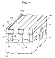
- FIG.1 shows a part of an integrated circuit in which the present invention is applied.
- the integrated circuit is a dynamic random access memory (DRAM) including a number of MOS transistors 1 and comprises a substrate 10 of doped silicon, a field oxide layer 11 provided on the substrate 10 for defining a region where the transistor is to be formed, and a doped diffusion region 12 formed in the substrate 10 between a pair of field oxide layers 11 as a source or drain region of the MOS transistor 1. Further, there are formed a gate oxide 13, a word line 14, a capacitor 15 and the like as illustrated.
- the integrated circuit is covered by an insulator layer 16 such as PSG or silica for electrical insulation as well as for surface protection.
- the present invention will be described with reference to such a DRAM device using the MOS transistor.
- the present invention is by no means limited to the DRAM device but is applicable to any other integrated circuits and devices.
- the insulator layer 16 is provided with a contact hole 17 in correspondence to the source, drain or gate of the transistor and the contact hole 17 is filled by a refractory metal 17a such as tungsten which is selectively grown on a part of the MOS transistor 1 exposed by the contact hole 17.
- a refractory metal 17a such as tungsten which is selectively grown on a part of the MOS transistor 1 exposed by the contact hole 17.
- the refractory metal 17a is preferentially deposited on a part of the semiconductor device exposed by the contact hole 17 rather than on the side wall of the contact hole 17 and there is no difficulty in filling the contact hole 17 from its bottom to the top by usual chemical vapor deposition and the like without creating void.
- the refractory metal filling the contact hole 17 is connected each other by a refractory metal conductor or wire extending above the insulator layer 16.
- a refractory metal conductor or wire extending above the insulator layer 16.
- another insulator layer 18 of PSG or silica is deposited on the insulator layer 16 and a groove 19 is formed in the insulator layer 16 in correspondence to a desired interconnection pattern so as to penetrate through the layer 18.
- the groove 19 exposes a top surface of the insulator layer 16 or a top surface of the refractory metal 17a filling the contact hole 17.
- a layer 19a of a material such as tungsten or tungsten silicide which acts as a nuclei for subsequent growth of the refractory metal is formed at the bottom of the groove 19 and a refractory metal strip or wire 19b is then grown in the groove 19 starting from its bottom using the layer 19a as the nuclei.
- the refractory metal wire 19b is grown from the bottom of the groove 19 to its top and undesirable formation of void or defects in the wire 19b due to the lateral growth of the refractory metal starting from the side wall of the groove 19 is effectively eliminated.
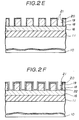
- FIGS.2(A) - (J) showing a part of the integrated circuit of FIG.1.
- the substrate 10 is covered by the field oxide layer 11 for device isolation and the semiconductor device such as MOS transistor 1 is formed as illustrated in FIG.1.
- the MOS transistor 1 is formed in a region outside of FIG.2(A) by well established process.
- the structure thus formed is covered by the PSG insulator layer 16 and the layer 16 is provided with the contact hole 17 which is filled by tungsten by a known procedure such as reduction of a source gas such as tungsten hexafluoride (WF 6 ) by using hydrogen or silane.
- WF 6 tungsten hexafluoride
- Such a contact hole is illustrated in FIG.1.
- the contact hole 17, too is formed in the region outside of FIG.2(A).
- the structure of FIG.2(A) is further covered by the insulator layer 18 which may also comprise PSG having a thickness of about 1.2 ⁇ m. Further, the PSG layer 18 is covered by a metal layer 20 of titanium sputtered thereon with a thickness of about 500 ⁇ .
- the groove 19 is formed so as to penetrate through the PSG layer 18 as well as through the titanium layer 20 according to the predetermined interconnection pattern by applying the reactive ion etching (RIE) process combined with known photolithographic patterning technique as shown in FIG.2(C) until a top surface of the underlying PSG layer 16 is exposed.
- RIE reactive ion etching
- FIG.2(E) it should be noted that titanium is left on a side wall of the groove 19 in a form of the layer 21 and at the top of the PSG layer in a form of the layer 20 which is previously deposited in the step of FIG.2(B).
- an amorphous silicon layer 22 is deposited on the entire structure of FIG.2(E) by sputtering for a thickness of about 1000 ⁇ as shown in FIG.2(F).
- the structure of FIG.2(F) is heat-treated in a nitrogen atmosphere at 620 °C for 60 seconds to react the titanium layers 20 and 21 with the amorphous silicon layer 22 to form a titanium silicide layer 21' as shown in FIG.2(G).
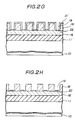
- This structure of FIG.2(G) is then dipped into a solution of hydrogen peroxide and ammonia held at 70°C whereby the titanium silicide layer 21' is selectively removed as shown in FIG.2(H).
- the amorphous silicon layer 22 extends substantially continuously along the groove.
- tungsten is deposited in the groove 19 by reduction of WF 6 , using hydrogen as reductant.
- the deposition is performed at 400°C and 0.2 Torr with a flow rate of 10 SCCM for WF 6 and 2 SLM for hydrogen.
- deposition of tungsten may be made by reduction of WF 6 by silane.
- the temperature of deposition may be set at 250 °C, the pressure at 3 X 10 -2 Torr, the flow rate of WF 6 at 3 SCCM and the flow rate of silane at 3 SCCM, together with a carrier gas of hydrogen with a flow rate set at 600 SCCM.
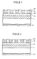
- a tungsten layer 23 fills the groove 19 starting from its bottom to its top as shown in FIG.2(I). Further, the structure of FIG.2(I) is heat treated at 900°C for 20 minutes to react the amorphous silicon layer 22 with tungsten layer 23 thereabove. As a result, there is formed a tungsten interconnection conductor wire 23' containing silicon and having an improved contact with the underlying PSG layer 16. Note that the wire 23' corresponds to the wire 10b of FIG.1.
- the tungsten conductor wire 23' thus grown in the groove already provided on the insulator layer 18 has various advantages such as substantially flat top surface suitable for multilevel interconnection as can be seen from FIG.2(J), substantially void-free structure as a result of the selective growth of tungsten proceeding from the bottom to the top of the groove, high yield by avoiding deposition of tungsten in a form of large sheet which tends to invite the separation of the tungsten sheet from the insulator layer underneath, and good electrical insulation between adjacent wires by directly growing the wires in the grooves.
- the metal layers 20 and 21 is not limited to titanium but other refractory metals such as tungsten, tantalum, molybdenum, cobalt, zirconium, hafnium and the like may also be used.
- the method of forming the layer 22 is not limited to sputtering of amorphous silicon but may be the chemical vapor deposition of polysilicon or amorphous silicon.
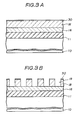
- FIGS.3(A) - (H) a second embodiment of the present invention will be described with reference to FIGS.3(A) - (H).
- these parts corresponding to those parts already described with reference to preceding drawings are given identical reference numerals and the description thereof will be omitted.
- the structure of FIG.2(A) serves for the initial structure of the process and in a step of FIG.3(A), a polysilicon layer 30 is deposited by chemical vapor deposition for a thickness of about 1000 ⁇ .
- a polysilicon layer 30 is deposited by chemical vapor deposition for a thickness of about 1000 ⁇ .
- the structure of FIG.3(A) is subjected to RIE in combination with photolithographic patterning to form the groove 19 such that the groove 19 penetrates through the layer 18 as well as through the polysilicon layer 30 as shown in FIG.3(B).
- a polysilicon layer 31 is deposited on the structure of FIG.3(B) for about 1000 ⁇ by chemical vapor deposition to form a structure of FIG.3(C), and a part of the polysilicon layer 31 at the top of the insulator layer 18 and at the bottom of the groove 19 is removed by RIE using a mixture of CF 4 and oxygen as the etching gas.
- FIG.3(D) a structure shown in which the polysilicon layer 31 is left only on the side wall of the groove 19.
- the top of the insulator layer 18 is also covered by the polysilicon layer 30 deposited at the step of FIG.3(A) and only the bottom of the groove 19 is exposed.
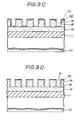
- a tungsten layer 32 is sputtered on the structure of FIG.3(D) for a thickness of about 1000 ⁇ to form a structure of FIG.3(E).
- the structure of FIG.3(E) is then heat-treated at 800 °C for 60 seconds so that the tungsten layer 32 is reacted with the polysilicon layers 30 and 31 covering the side wall of the groove 19 as well as the top of the insulator layer 18 and there is formed a tungsten silicide layer 31' as shown in FIG.3(F). Note that the tungsten layer 32 at the bottom of the groove is substantially free from reaction as there is no immediate source of silicon in the vicinity of the layer 32.
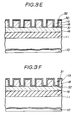
- FIG.3(F) is subjected to an isotropic plasma etching using sulfur hexafluoride (SF 6 ) as the etching gas to remove the silicide layer 31' selectively.
- SF 6 sulfur hexafluoride
- FIG.3(G) a structure shown in FIG.3(G) where the tungsten layer 32 is left only at the bottom of the groove 19 is obtained.
- the isotropic plasma etching employed in this step causes also the removal of layer 32 to some extent. However, such an unwanted etching of the layer 32 can be minimized by suitably choosing the condition of etching.
- the etching may be performed at 0.2 Torr while flowing SF 6 at a flow rate of 25 SCCM and while applying a radio frequency power of 0.4 W/cm 2 .
- FIG.3(G) is subjected to heat treatment at 900°C for 10 minutes and thereafter the deposition of tungsten in the groove 19 is performed using the tungsten layer 32 at the bottom of the groove 19 as the nuclei of crystal growth.
- the deposition is made by reduction of WF 6 by hydrogen or silane similarly to the case of the first embodiment.
- FIG.3(H) where the groove 19 is filled completely by a tungsten interconnection wire 33 is obtained in correspondence to the structure of FIG.1.
- the parts corresponding to these parts already described with reference to preceding drawings are given identical reference numerals and the description thereof will be omitted.
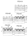
- FIG.4(A) the structure of FIG.2(A) serving for the initial structure of the process is deposited with a photoresist 40 and patterned according to the desired interconnection pattern.
- the structure is subjected to anisotropic etching using RIE such that there is formed the groove 19 according to the desired interconnection pattern as shown in FIG.4(B).
- the groove 19 connects the contact holes 17 (FIG.1) provided to penetrate through the insulator layer 16 in correspondence to the semiconductor devices which are already filled by refractory metal such as tungsten.
- the photoresist 40 is already removed after etching.
- FIG.4(B) the structure of FIG.4(B) is covered by a polysilicon layer 41 deposited by chemical vapor deposition for example with a thickness of about 1000 ⁇ . Further, the polysilicon layer 41 is subjected to oxidization by heat treatment whereby a silica layer 42 having a thickness of about 700 ⁇ is formed on its top surface as illustrated in FIG.4(C). Obviously, the thickness of the layers 41 and 42 are substantially smaller than the depth of the groove 19 penetrating the insulator layer 18 and there holds a relation d 1 + d 2 ⁇ D where d 1 stands for the thickness of the layer 41, d 2 stands for the thickness of the layer 42, and D stands for the thickness of the layer 18.
- FIG.4(D) the structure of FIG.4(C) is coated by a polymer layer 43 such as photoresist which is then baked at a predetermined temperature. Further, the polymer layer 43 is subjected to ashing by an oxygen plasma process until the silica layer 42 at the top of the insulator layer 18 is exposed. As a result, a structure shown in FIG.4(E) in which the groove 19 is filled by the polymer layer 43 is obtained. Next, the silica layer 42 is removed by isotropic etching using the polymer layer 43 as the mask.
- a polymer layer 43 such as photoresist
- the etching may be performed by dipping the structure of FIG.4(E) in a buffered solution of hydrofluoric acid and a structure shown in FIG.4(F) is obtained.
- the polysilicon layer 41 is exposed at the top of the insulator layer 18 as well as at the side wall of the groove 19.
- the anisotropic etching process such as RIE using CF 4 and CHF 3 as the etching gas. Small amount of silica remaining at at the bottom part of the groove 19 along its side wall is tolerable.
- the polymer layer 43' in the groove 19 is removed by oxygen plasma process such that the silica layer 42 protected by the polymer layer 43' at the bottom of the groove 19 is now exposed as shown in FIG.4(G).
- the polysilicon layer 41 is removed from the top of the insulator layer 18 as well as from the side wall of the groove 19. This process may be performed by isotropic plasma etching using etching gas such as CF 4 . As a result, a structure shown in FIG.4(H) is obtained.
- FIG.4(H) is dipped in a buffered solution of hydrofluoric acid to remove the silica layer 7 remaining at the bottom of the groove 19.
- a structure shown in FIG.4(I) wherein the polysilicon layer 41 is exposed at the bottom of the groove 19 is obtained.
- tungsten is grown in the groove 19 from its bottom to the top as shown in FIG.4(J) in which the groove 19 is filled by a tungsten interconnection wire 44 corresponding to the wire 19b of FIG.1.
- Such a filling of the groove 19 by tungsten may be performed by the reduction of WF 6 by hydrogen or silane similarly to the case of the first and second embodiments.
- the obtained wire 44 filling the groove 19 is substantially free from void and a reliable interconnection is achieved.
- the growth of the tungsten interconnection conductor wire is made from the bottom to the top of the groove without creating void as there occurs no lateral growth of tungsten at the top or intermediate part of the groove.
- the conductor wire thus obtained is dense and fills the groove up to its top opening.
- the material used for the interconnection wire is not limited to tungsten but other refractory metals such as molybdenum, titanium, tantalum may be used as well. When molybdenum is used, molybdenum hexafluoride (MoF 6 ) may be used for the source gas.
- titanium when titanium is used, titanium tetrachloride (TiCl 4 ) may be used for the source gas. Further, when tantalum is used, tantalum pentachloride (TaCl 5 ) may be used for the source gas. In any of these, a high yield is obtained because of the selective growth which occurs only in the groove and produces less mechanical stress with respect to the insulator layer underneath.
- the method of providing the nuclei 19a at the bottom of the groove may be performed by ion implantation of elements such as silicon at the time when the groove 19 is formed by using the photoresist for defining the groove 19 as the mask.
Landscapes
- Internal Circuitry In Semiconductor Integrated Circuit Devices (AREA)
Claims (11)
- Verfahren zum Herstellen einer integrierten Halbleiterschaltung umfassend:gekennzeichnet durch die Schrittemindestens eine auf einem Substrat (10) ausgebildete Halbleiteranordnung (1), eine auf das Substrat aufgebrachte Isolierschicht (16), welche die Halbleiteranordnung bedeckt,ein durch die Isolierschicht verlaufendes Kontaktloch (17), um einen gewünschten Teil der Halbleiteranordnung freizulegen, wobei das Kontaktloch zur elektrischen Verbindung mit einem hochschmelzenden Metall (17a) gefüllt ist, undeine die erste Isolierschicht bedeckende zweite Isolierschicht (18),Ausbilden einer durch die zweite Isolierschicht (18) verlaufenden Rille (19) gemäß einem bestimmten Verbindungsmuster, so daß die Rille über mindestens ein Kontaktloch (17) verläuft und eine Oberfläche des das Kontaktloch ausfüllenden hochschmelzenden Metalls (17a) und eine Oberfläche der ersten Isolierschicht (16) durch die Rille freigelegt werden, und Ausbilden einer Materialschicht (19a) auf einem Boden der Rille, wobei die Materialschicht im wesentlichen ununterbrochen entlang der Rille verläuft und als Kern für den Kristallwachstum eines zweiten hochschmelzenden Metalls dient,wobei der Schritt der Ausbildung der als Kern dienenden Materialschicht (19a) die Schritte umfaßt:Aufbringen eines ersten Materials (21; 31), so daß eine Seitenwand und der Boden der Rille bedeckt werden,selektives Entfernen des ersten Materials von dem Boden der Rille durch Ätzen,Aufbringen eines die Materialschicht bildenden zweiten Materials (22, 32), so daß die Seitenwand und der Boden der Rille bedeckt werden,Herbeiführen einer Reaktion des ersten Materials mit dem zweiten Material, um eine die Seitenwand der Rille (19, 52) bedeckende Verbundschicht (21', 31') auszubilden,selektives Entfernen des ersten und zweiten Materials von der Seitenwand der Rille durch selektives Entfernen der Verbundschicht von der Seitenwand durch Ätzen, undAufbringen des zweiten hochschmelzenden Metalls in der Rille, so daß das zweite hochschmelzende Metall mit der freigelegten Oberfläche des hochschmelzenden Metalls einen elektrischen Kontakt bildet, bis die Rille im wesentlichen mit einem aus dem zweiten hochschmelzenden Metall bestehenden Leiter (19b) gefüllt ist.
- Verfahren nach Anspruch 1,
dadurch gekennzeichnet,daß der Schritt des Aufbringens des ersten Materials (20; 31) nach dem Schritt des Ausbildens der Rille des weiteren die aufeinanderfolgenden Schritte Aufbringen des ersten Materials auf die die Rille aufweisende zweite Isolierschicht (18), um eine Oberfläche der zweiten Isolierschicht, die Seitenwand der Rille und den Boden der Rille zu bedecken, umfaßt, unddaß der Schritt des selektiven Entfernens des ersten Materials von dem Boden der Rille die aufeinanderfolgenden Schritte selektives Entfernen des ersten Materials von der Oberfläche der zweiten Isolierschicht und von dem Boden der Rille durch anisotropes Ätzen umfaßt. - Verfahren nach Anspruch 2,
dadurch gekennzeichnet,daß das Verfahren des weiteren einen Schritt Aufbringen einer weiteren Schicht des ersten Materials (20, 30) unmittelbar auf die zweite Isolierschicht (18) vor dem Schritt des Ausbildens der Rille (19) umfaßt, um eine erste Materialschicht (20, 30) auszubilden,daß der Schritt des Entfernens des ersten Materials (21, 31) ausgeführt wird, um die somit unmittelbar auf der zweiten Isolierschicht vorhandene weitere Schicht des ersten Materials freizulegen,daß durch den Schritt des Aufbringens des zweiten Materials (22, 32) das zweite Material nicht nur auf die Seitenwand und den Boden der Rille, sondern auch auf die somit freigelegte weitere Schicht des ersten Materials aufgebracht wird,daß der Schritt des Herbeiführens einer Reaktion des ersten Materials mit dem zweiten Material des weiteren als Resultat der Reaktion zwischen dem ersten Material und dem zweiten Material die Ausbildung einer Verbundschicht (21', 31') an der Oberfläche der zweiten Isolierschicht herbeiführt, unddaß der Schritt des selektiven Entfernens des ersten Materials des weiteren das Entfernen der Verbundschicht von der Oberfläche der Isolierschicht herbeiführt, wobei die Oberfläche der zweiten Isolierschicht freigelegt wird. - Verfahren nach einem der Ansprüche 1 bis 3,
dadurch gekennzeichnet,daß das erste Material (21) ein Material umfaßt, welches bei Reaktion mit Silizium ein Silizid ausbilden kann, unddaß das zweite Material (22) Silizium umfaßt. - Verfahren nach Anspruch 4,
dadurch gekennzeichnet,
daß das erste Material (21) aus einer Gruppe ausgewählt wird, welche Titan, Wolfram, Tantal, Molybdän, Kobalt, Zirkonium und Hafnium umfaßt. - Verfahren nach einem der Ansprüche 1 bis 4,
dadurch gekennzeichnet,daß das erste Material (31) Silizium umfaßt, unddaß das zweite Material (32) aus einer Gruppe ausgewählt wird, welche Titan, Wolfram, Tantal, Molybdän, Kobalt, Zirkonium und Hafnium umfaßt. - Verfahren zum Herstellen einer integrierten Halbleiterschaltung umfassend:gekennzeichnet durch die Schrittemindestens eine auf einem Substrat (10) ausgebildete Halbleiteranordnung (1),eine auf das Substrat aufgebrachte Isolierschicht (16), welche die Halbleiteranordnung bedeckt,ein durch die Isolierschicht verlaufendes Kontaktloch (17), um einen gewünschten Teil der Halbleiteranordnung freizulegen, wobei das Kontaktloch zur elektrischen Verbindung mit einem hochschmelzenden Metall (17a) gefüllt ist, undeine die erste Isolierschicht bedeckende zweite Isolierschicht (18),undAusbilden einer durch die zweite Isolierschicht (18) verlaufenden Rille (19, 52) gemäß einem bestimmten Verbindungsmuster, so daß die Rille über mindestens ein Kontaktloch (17) verläuft und eine Oberfläche des das Kontaktloch ausfüllenden hochschmelzenden Metalls (17a) und eine Oberfläche der ersten Isolierschicht (16) durch die Rille freigelegt werden, und Ausbilden einer Materialschicht (19a) auf einem Boden der Rille, wobei die Materialschicht im wesentlichen ununterbrochen entlang der Rille verläuft und als Kern für den Kristallwachstum eines zweiten hochschmelzenden Metalls dient,wobei der Schritt der Ausbildung der als Kern dienenden Materialschicht (19a) die Schritte umfaßt:Aufbringen eines die Materialschicht bildenden ersten Materials (41), so daß eine Seitenwand und der Boden der Rille bedeckt werden,selektives Entfernen des ersten Materials von der Seitenwand der Rille durchselektives Bedecken der Materialschicht (19a) am Boden der Rille (19, 52) mit einer Maske (42) durch Vorsehen der Maske (42) gleichmäßig auf dem ersten Material (41) nach dem Schritt des Aufbringens des ersten Materials, Füllen der Rille (19) mit einer organischen Substanz (43'), Entfernen eines Teils der die Seitenwand bedeckenden Maske durch Ätzen unter Verwendung der organischen Substanz als weitere Maske und Entfernen der organischen Substanz von der Rille,Entfernen eines nicht von der Maske bedeckten Teils der Materialschicht durch Ätzen, undEntfernen der Maske,Aufbringen des zweiten hochschmelzenden Metalls in der Rille, so daß das zweite hochschmelzende Metall mit der freigelegten Oberfläche des hochschmelzenden Metalls einen elektrischen Kontakt bildet, bis die Rille im wesentlichen mit einem aus dem zweiten hochschmelzenden Metall bestehenden Leiter (19b) gefüllt ist.
- Verfahren nach Anspruch 7,
dadurch gekennzeichnet,
daß das erste Material (41) Silizium und die Maske (42) durch Wärmeoxidation des ersten Materials ausgebildetes Silika umfaßt. - Verfahren nach einem der Ansprüche 1 bis 8,
dadurch gekennzeichnet,
daß die erste und zweiten Isolierschicht (16, 18) Phosphosilikatglas umfassen. - Verfahren nach einem der Ansprüche 1 bis 8,
dadurch gekennzeichnet,
daß die erste und zweite Isolierschicht (16, 18) Silika umfassen. - Verfahren nach einem der Ansprüche 1 bis 10,
dadurch gekennzeichnet,
daß das erste und zweite hochschmelzende Metall (17a, 19b) aus einer Gruppe ausgewählt werden, welche Wolfram, Molybdän, Titan und Tantal umfaßt.
Priority Applications (1)
| Application Number | Priority Date | Filing Date | Title |
|---|---|---|---|
| EP95105869A EP0665589B1 (de) | 1988-09-07 | 1989-09-06 | Herstellungsverfahren für eine integrierte Halbleiterschaltung mit einem Verbundungsleiter, der in einer Schutzschicht auf der integriertere Halbleiterschaltung eingebettet ist |
Applications Claiming Priority (6)
| Application Number | Priority Date | Filing Date | Title |
|---|---|---|---|
| JP222273/88 | 1988-09-07 | ||
| JP63222273A JPH0738391B2 (ja) | 1988-09-07 | 1988-09-07 | 半導体装置の製造方法 |
| JP289208/88 | 1988-11-16 | ||
| JP63289208A JPH02134823A (ja) | 1988-11-16 | 1988-11-16 | 半導体装置の製造方法 |
| JP326687/88 | 1988-12-23 | ||
| JP63326687A JPH02170536A (ja) | 1988-12-23 | 1988-12-23 | 半導体装置 |
Related Child Applications (2)
| Application Number | Title | Priority Date | Filing Date |
|---|---|---|---|
| EP95105869.2 Division-Into | 1989-09-06 | ||
| EP95105869A Division EP0665589B1 (de) | 1988-09-07 | 1989-09-06 | Herstellungsverfahren für eine integrierte Halbleiterschaltung mit einem Verbundungsleiter, der in einer Schutzschicht auf der integriertere Halbleiterschaltung eingebettet ist |
Publications (2)
| Publication Number | Publication Date |
|---|---|
| EP0359109A1 EP0359109A1 (de) | 1990-03-21 |
| EP0359109B1 true EP0359109B1 (de) | 1998-07-22 |
Family
ID=27330647
Family Applications (2)
| Application Number | Title | Priority Date | Filing Date |
|---|---|---|---|
| EP95105869A Expired - Lifetime EP0665589B1 (de) | 1988-09-07 | 1989-09-06 | Herstellungsverfahren für eine integrierte Halbleiterschaltung mit einem Verbundungsleiter, der in einer Schutzschicht auf der integriertere Halbleiterschaltung eingebettet ist |
| EP89116458A Expired - Lifetime EP0359109B1 (de) | 1988-09-07 | 1989-09-06 | Verfahren zum Herstellen einer integrierten Halbleiterschaltung mit einem in einer Schutzschicht integrierten Verbindungsleiter |
Family Applications Before (1)
| Application Number | Title | Priority Date | Filing Date |
|---|---|---|---|
| EP95105869A Expired - Lifetime EP0665589B1 (de) | 1988-09-07 | 1989-09-06 | Herstellungsverfahren für eine integrierte Halbleiterschaltung mit einem Verbundungsleiter, der in einer Schutzschicht auf der integriertere Halbleiterschaltung eingebettet ist |
Country Status (4)
| Country | Link |
|---|---|
| US (1) | US4983543A (de) |
| EP (2) | EP0665589B1 (de) |
| KR (1) | KR920006573B1 (de) |
| DE (2) | DE68928748T2 (de) |
Families Citing this family (12)
| Publication number | Priority date | Publication date | Assignee | Title |
|---|---|---|---|---|
| JPH038359A (ja) * | 1989-06-06 | 1991-01-16 | Fujitsu Ltd | 半導体装置の製造方法 |
| JPH03190232A (ja) * | 1989-12-20 | 1991-08-20 | Fujitsu Ltd | 半導体装置の製造方法 |
| KR0176715B1 (ko) * | 1990-07-30 | 1999-04-15 | 오가 노리오 | 드라이에칭방법 |
| GB9105943D0 (en) * | 1991-03-20 | 1991-05-08 | Philips Nv | A method of manufacturing a semiconductor device |
| US5453154A (en) * | 1991-10-21 | 1995-09-26 | National Semiconductor Corporation | Method of making an integrated circuit microwave interconnect and components |
| JP3216345B2 (ja) * | 1993-04-06 | 2001-10-09 | ソニー株式会社 | 半導体装置及びその作製方法 |
| JPH0922896A (ja) * | 1995-07-07 | 1997-01-21 | Toshiba Corp | 金属膜の選択的形成方法 |
| US5950099A (en) * | 1996-04-09 | 1999-09-07 | Kabushiki Kaisha Toshiba | Method of forming an interconnect |
| US5792705A (en) * | 1996-06-28 | 1998-08-11 | Taiwan Semiconductor Manufacturing Company, Ltd. | Optimized planarization process for SOG filled vias |
| CN1055788C (zh) * | 1997-03-14 | 2000-08-23 | 联华电子股份有限公司 | 在半导体器件内制作内连线的方法 |
| US6281114B1 (en) * | 2000-02-07 | 2001-08-28 | Infineon Technologies Ag | Planarization after metal chemical mechanical polishing in semiconductor wafer fabrication |
| US6365428B1 (en) * | 2000-06-15 | 2002-04-02 | Sandia Corporation | Embedded high-contrast distributed grating structures |
Family Cites Families (9)
| Publication number | Priority date | Publication date | Assignee | Title |
|---|---|---|---|---|
| JPS5487175A (en) * | 1977-12-23 | 1979-07-11 | Cho Lsi Gijutsu Kenkyu Kumiai | Method of fabricating semiconductor |
| US4617193A (en) * | 1983-06-16 | 1986-10-14 | Digital Equipment Corporation | Planar interconnect for integrated circuits |
| JPS60115245A (ja) * | 1983-11-28 | 1985-06-21 | Toshiba Corp | 半導体装置の製造方法 |
| US4584207A (en) * | 1984-09-24 | 1986-04-22 | General Electric Company | Method for nucleating and growing tungsten films |
| JPS61139026A (ja) * | 1984-12-11 | 1986-06-26 | Fujitsu Ltd | 半導体装置の製造方法 |
| JPS62141740A (ja) * | 1985-12-16 | 1987-06-25 | Matsushita Electric Ind Co Ltd | 半導体集積回路の製造方法 |
| EP0257948A3 (de) * | 1986-08-25 | 1988-09-28 | AT&T Corp. | Durchgangsleitung für CMOS-Anordnungen |
| US4746621A (en) * | 1986-12-05 | 1988-05-24 | Cornell Research Foundation, Inc. | Planar tungsten interconnect |
| US4764484A (en) * | 1987-10-08 | 1988-08-16 | Standard Microsystems Corporation | Method for fabricating self-aligned, conformal metallization of semiconductor wafer |
-
1989
- 1989-09-01 US US07/401,690 patent/US4983543A/en not_active Expired - Fee Related
- 1989-09-06 DE DE68928748T patent/DE68928748T2/de not_active Expired - Fee Related
- 1989-09-06 DE DE68928873T patent/DE68928873T2/de not_active Expired - Fee Related
- 1989-09-06 EP EP95105869A patent/EP0665589B1/de not_active Expired - Lifetime
- 1989-09-06 EP EP89116458A patent/EP0359109B1/de not_active Expired - Lifetime
- 1989-09-07 KR KR1019890012954A patent/KR920006573B1/ko not_active Expired
Also Published As
| Publication number | Publication date |
|---|---|
| EP0665589A2 (de) | 1995-08-02 |
| DE68928748D1 (de) | 1998-08-27 |
| DE68928748T2 (de) | 1999-02-18 |
| DE68928873T2 (de) | 1999-06-24 |
| KR920006573B1 (ko) | 1992-08-08 |
| EP0665589B1 (de) | 1998-12-02 |
| EP0359109A1 (de) | 1990-03-21 |
| DE68928873D1 (de) | 1999-01-14 |
| EP0665589A3 (de) | 1996-01-03 |
| US4983543A (en) | 1991-01-08 |
| KR900005574A (ko) | 1990-04-14 |
Similar Documents
| Publication | Publication Date | Title |
|---|---|---|
| EP0279588B1 (de) | Kontakt in einer Bohrung in einem Halbleiter und Verfahren zu seiner Herstellung | |
| US4874719A (en) | Method for manufacturing an electrical connection between conductor levels | |
| US5795811A (en) | Method for forming insulating films in semiconductor devices | |
| US7659630B2 (en) | Interconnect structures with interlayer dielectric | |
| US8580666B2 (en) | Methods of forming conductive contacts | |
| US5476814A (en) | Method of manufacturing semiconductor device utilizing selective CVD method | |
| EP0383610B1 (de) | Verfahren zum Herstellen einer Halbleitervorrichtung | |
| US6482741B1 (en) | Copper wiring structure comprising a copper material buried in a hollow of an insulating film and a carbon layer between the hollow and the copper material in semiconductor device and method fabricating the same | |
| EP0424485B1 (de) | Vollverdiefte verbindungsstruktur mit titanium/wolfram und selektivem cvd-wolfram | |
| EP0359109B1 (de) | Verfahren zum Herstellen einer integrierten Halbleiterschaltung mit einem in einer Schutzschicht integrierten Verbindungsleiter | |
| US5071789A (en) | Method for forming a metal electrical connector to a surface of a semiconductor device adjacent a sidewall of insulation material with metal creep-up extending up that sidewall, and related device | |
| US6888252B2 (en) | Method of forming a conductive contact | |
| US20030157788A1 (en) | Method of suppressing void formation in a metal line | |
| US6696368B2 (en) | Titanium boronitride layer for high aspect ratio semiconductor devices | |
| US6475907B1 (en) | Semiconductor device having a barrier metal layer and method for manufacturing the same | |
| US6852579B2 (en) | Method of manufacturing a semiconductor integrated circuit device | |
| US6159835A (en) | Encapsulated low resistance gate structure and method for forming same | |
| US7126178B2 (en) | Semiconductor device and its manufacturing method | |
| US5366928A (en) | Method of manufacturing a semiconductor device, in which a metal conductor track is provided on a surface of a semiconductor body | |
| JP2573621B2 (ja) | 電気的相互接続部の製造方法 | |
| JPS6362107B2 (de) | ||
| JP2702007B2 (ja) | 半導体装置の製造方法 | |
| JPH0234957A (ja) | 半導体装置の製造方法 | |
| JPH02241032A (ja) | 配線形成方法 | |
| JPH079893B2 (ja) | 半導体装置の製造方法 |
Legal Events
| Date | Code | Title | Description |
|---|---|---|---|
| PUAI | Public reference made under article 153(3) epc to a published international application that has entered the european phase |
Free format text: ORIGINAL CODE: 0009012 |
|
| AK | Designated contracting states |
Kind code of ref document: A1 Designated state(s): DE FR GB |
|
| ITCL | It: translation for ep claims filed |
Representative=s name: STUDIO JAUMANN |
|
| 17P | Request for examination filed |
Effective date: 19900921 |
|
| 17Q | First examination report despatched |
Effective date: 19940209 |
|
| RIN1 | Information on inventor provided before grant (corrected) |
Inventor name: MOTOYAMA, TAKUSHI Inventor name: SATO, YASUHISA |
|
| GRAG | Despatch of communication of intention to grant |
Free format text: ORIGINAL CODE: EPIDOS AGRA |
|
| GRAG | Despatch of communication of intention to grant |
Free format text: ORIGINAL CODE: EPIDOS AGRA |
|
| GRAH | Despatch of communication of intention to grant a patent |
Free format text: ORIGINAL CODE: EPIDOS IGRA |
|
| RBV | Designated contracting states (corrected) | ||
| GRAH | Despatch of communication of intention to grant a patent |
Free format text: ORIGINAL CODE: EPIDOS IGRA |
|
| GRAA | (expected) grant |
Free format text: ORIGINAL CODE: 0009210 |
|
| AK | Designated contracting states |
Kind code of ref document: B1 Designated state(s): DE |
|
| DX | Miscellaneous (deleted) | ||
| REF | Corresponds to: |
Ref document number: 68928748 Country of ref document: DE Date of ref document: 19980827 |
|
| RIN2 | Information on inventor provided after grant (corrected) |
Free format text: SATO, YASUHISA * MOTOYAMA, TAKUSHI |
|
| PLBE | No opposition filed within time limit |
Free format text: ORIGINAL CODE: 0009261 |
|
| STAA | Information on the status of an ep patent application or granted ep patent |
Free format text: STATUS: NO OPPOSITION FILED WITHIN TIME LIMIT |
|
| 26N | No opposition filed | ||
| PGFP | Annual fee paid to national office [announced via postgrant information from national office to epo] |
Ref country code: DE Payment date: 19990906 Year of fee payment: 11 |
|
| PG25 | Lapsed in a contracting state [announced via postgrant information from national office to epo] |
Ref country code: DE Free format text: LAPSE BECAUSE OF NON-PAYMENT OF DUE FEES Effective date: 20010601 |