EP0357799B1 - Vorrichtung und verfahren zur modulierung eines halbleiterlasers - Google Patents
Vorrichtung und verfahren zur modulierung eines halbleiterlasers Download PDFInfo
- Publication number
- EP0357799B1 EP0357799B1 EP89903271A EP89903271A EP0357799B1 EP 0357799 B1 EP0357799 B1 EP 0357799B1 EP 89903271 A EP89903271 A EP 89903271A EP 89903271 A EP89903271 A EP 89903271A EP 0357799 B1 EP0357799 B1 EP 0357799B1
- Authority
- EP
- European Patent Office
- Prior art keywords
- light
- semiconductor laser
- modulation
- output
- phase
- Prior art date
- Legal status (The legal status is an assumption and is not a legal conclusion. Google has not performed a legal analysis and makes no representation as to the accuracy of the status listed.)
- Expired - Lifetime
Links
Images


Classifications
-
- H—ELECTRICITY
- H04—ELECTRIC COMMUNICATION TECHNIQUE
- H04B—TRANSMISSION
- H04B10/00—Transmission systems employing electromagnetic waves other than radio-waves, e.g. infrared, visible or ultraviolet light, or employing corpuscular radiation, e.g. quantum communication
- H04B10/50—Transmitters
-
- H—ELECTRICITY
- H04—ELECTRIC COMMUNICATION TECHNIQUE
- H04L—TRANSMISSION OF DIGITAL INFORMATION, e.g. TELEGRAPHIC COMMUNICATION
- H04L27/00—Modulated-carrier systems
- H04L27/10—Frequency-modulated carrier systems, i.e. using frequency-shift keying
- H04L27/12—Modulator circuits; Transmitter circuits
-
- H—ELECTRICITY
- H04—ELECTRIC COMMUNICATION TECHNIQUE
- H04L—TRANSMISSION OF DIGITAL INFORMATION, e.g. TELEGRAPHIC COMMUNICATION
- H04L27/00—Modulated-carrier systems
- H04L27/18—Phase-modulated carrier systems, i.e. using phase-shift keying
- H04L27/20—Modulator circuits; Transmitter circuits
- H04L27/2096—Arrangements for directly or externally modulating an optical carrier
-
- H—ELECTRICITY
- H01—ELECTRIC ELEMENTS
- H01S—DEVICES USING THE PROCESS OF LIGHT AMPLIFICATION BY STIMULATED EMISSION OF RADIATION [LASER] TO AMPLIFY OR GENERATE LIGHT; DEVICES USING STIMULATED EMISSION OF ELECTROMAGNETIC RADIATION IN WAVE RANGES OTHER THAN OPTICAL
- H01S5/00—Semiconductor lasers
- H01S5/06—Arrangements for controlling the laser output parameters, e.g. by operating on the active medium
- H01S5/068—Stabilisation of laser output parameters
- H01S5/0683—Stabilisation of laser output parameters by monitoring the optical output parameters
- H01S5/06832—Stabilising during amplitude modulation
Definitions
- the present invention relates to a semiconductor laser apparatus for sending an optical signal modulated in accordance with transmission data, comprising: a semiconductor laser having applied a bias current; modulating current generating means for generating drive current pulse applied to the semiconductor laser to directly modulate a phase of output light of the semiconductor laser; and superimposing means for superimposing the drive current on the bias current.
- a semiconductor laser apparatus of this kind is known from JP-A-60235543.
- Modulation methods are basically divided into two types: those for directly modulating a driving current of a semiconductor laser using transmission data, namely, direct modulation methods, and those for indirectly modulating the output light from the semiconductor laser using an external modulator, namely, external modulation methods.
- a commonly used prior-art direct modulation system uses a threshold current I T of a semiconductor laser as a bias current, and superimposes on the bias current a modulation current which is responsive to transmission data, thereby driving the semiconductor laser.
- the semiconductor laser must be driven by a pulse current with a relatively large amplitude. This produces chirping (i.e., a dynamic wavelength shift) at an oscillation wavelength, which distorts the wave form of the optical pulse propagating in the optical filter. This causes the problem that it is difficult to conduct direct modulations by using a driving current of high-speed data of several to several tens of Gb/s. Further, as the modulation amplitude is large, a large load is imposed on both the semiconductor laser and the driving circuit thereof.
- a constant bias current I0 which is larger by a sufficient margin than the threshold current I T of the laser, is applied to the modulating current I m , which is typically ⁇ several tens of milliamperes.
- the modulating current I m which is typically ⁇ several tens of milliamperes.
- Prior-art external modulation methods use various kinds of external modulators, such as those using electro-optical-effect material and acoustic-optical-effect material, those of the waveguide path type, and those of the light-deflection type. Therefore, there is a problem that external modulators produce a large loss upon connection, thus necessitating a complicated structure for high-speed modulation.
- FIG. 2 The structure of an optical interferometer 10 using a commonly used Mach-Zehnder-type electro-optical modulator as the external modulator of the semiconductor laser, is shown in Fig. 2.
- a constant light beam is input from a semiconductor laser to a single optical waveguide path 1 at the input side of the interferometer 10. This light is divided into two beams which pass two optical waveguide paths 2 and 3. Thereafter these beams are combined to form a single optical waveguide path 4.
- Electrodes 5 and 6 are provided to the two optical waveguide paths 2 and 3, and the difference in optical path length is varied by applying a suitable voltage to them, thereby creating a phase difference between the two beams to be combined.
- the two light beams are caused to interfere with each other upon recombining, producing an output light which is subject to intensity modulation in accordance with the phase difference between the two beams.
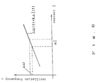
- Such an optical interferometer 10 has the problem that the actual length of the light path varies with temperature, and that the wavelength of an input light itself varies. This causes the phase difference between the two lights to be combined to vary with time, so that a reference point of an operation (a point of phase bias voltage) for an intensity modulation is unstable with time.
- a demodulation technique of a phase modulated laser beam is known.
- An interferometer is used for demodulating a frequency shift keyed signal.
- an object of the present invention is to provide a semiconductor laser apparatus for sending an optical signal light intensity modulated in accordance with the transmission data which eliminates the adverse influence of chirping, and which decreases loads of the semiconductor laser and its driving circuit, thereby enabling a high speed, direct modulation in a stable manner.
- the drive current is determined based on the product of an oscillation wavelength chirping coefficient of the semiconductor laser and an integral of the drive current value during one time slot of the transmission data being ⁇ or - ⁇ .
- the oscillation angular frequency ⁇ of the semiconductor laser can be considered to vary in proportion to the change ⁇ I in the current I near the average driving current.
- the change ⁇ I(t) in the driving current is used as a modulation current pulse.
- the product of a time integral for a single time slot T of ⁇ I(t) and a chirping coefficient (k) is determined to be ⁇ or - ⁇ . Namely,
- Equation (1) When equation (1) is established, the phase ⁇ is reversed by ⁇ or - ⁇ during one time slot in correspondence with a modulation current pulse. Therefore, by producing a modulation current pulse ⁇ I(t) at a time corresponding to an existence of a transmission data signal, a phase modulation between 0 and ⁇ can be applied to an output light of the semiconductor laser.
- any form of ⁇ I(t) can be used providing ⁇ I(t) has a narrow time region and the integral thereof is equal to ⁇ /k or - ⁇ /k.
- the spread of oscillation wavelength is limited to sidebands resulting from a modulation and the adverse affect of chirping caused by conventional direct modulation can be avoided.
- the semiconductor laser is subject to a small-amplitude modulation and the loads of both the semiconductor laser and its driving circuit can be greatly reduced.
- a high-speed modulation exceeding the frequency limitation of conventional direct modulation can be realized.
- the light output of the semiconductor laser which is subject to a phase modulation between 0 and ⁇ as recited above, is introduced into a self-homodyne-type optical interferometer.
- Amplitude modulation is produced by a self-homodyne-type method in accordance with the respective phase differences, and the output light is converted into a light pulse of "0" or "1".
- high-speed light intensity modulation is made possible.
- the output light is intensity-modulated to "1" and "0", respectively.
- respective probabilities of both these values are generally one half, and if it is considered that the light intensity is moved instantaneously between "1” and "0", the average intensity of the two lights becomes "1/2".
- the phase difference is moved between ⁇ 1′ and ⁇ 2′ as shown in Fig.
- an average intensity is obtained by integrating the intensity of the output light from an optical interferometer in a time interval corresponding to a speed which is slower than the modulation speed (for example, a time interval of 1/100 sec for a phase modulation of lGb/s).
- a scattering of transmission data "1" and "0" is compensated and a fully accurate value can be obtained.
- Deviation of a phase bias can be easily detected by a variation in average intensity as recited above and a feedback can be applied to counteract the deviation, thereby greatly stabilizing the output from the light interferometer.
- the light modulation apparatus of the present invention comprises a code conversion portion, a differentiation circuit, a semiconductor laser and a light interferometer.
- the sign conversion portion outputs a signal with a reversed sign only when the transmission data is "1", and produces a signal with the previous sign when the transmission data is "0" (an operation opposite to the above is also accepted).
- the conversion output signal is differentiated by a differentiation circuit.
- a source of a bias current supplies to a semiconductor laser a bias current selected such that the semiconductor laser provides an output light of the desired optical intensity when the semiconductor laser is subject to an oscillation and the differentiation output signal from the differentiation circuit is overlapped or superimposed on the bias current as a modulation current pulse.
- the phase of the output light of the semiconductor laser is varied by the modulation current pulse.
- the above modulation current pulse is selected such that the phase shift or change becomes ⁇ or - ⁇ .
- the optical interferometer has a construction in which a self-homodyne is possible and has a light delay circuit for providing a relative delay time corresponding to one time slot and a relative phase difference of 0 or ⁇ .
- the output light of the optical interferometer becomes "0" or "1".
- the semiconductor laser is put in a state of continuous oscillation and the modulation current is small compared with the constant bias current, thereby overcoming the chirping problem.
- the optical interferometer obtains an output light subject to an intensity modulation in accordance with a phase change in the output light of the semiconductor laser. It has a small connection loss and can operate at an extremely high speed. Therefore, a high-speed signal of several to several tens of Gb/s can be intensity-modulated in a stable manner.
- Figures 4A and 4B show whole constructions in which the present invention is applied to an optical communication system.
- the optical interferometer 12 of the present invention may be provided after the semiconductor laser 11 on the transmission side and before the transmission light fiber 13 as shown in Fig. 4A.
- the light interferometer 12 is provided after the transmission light fiber 13 and before the receiver 14 on the receiving side.
- the optical interferometer 12 is provided on the transmission side as shown in Fig. 4A, it is possible to apply a feedback to an oscillation wavelength of the semiconductor laser 11 or to apply a feedback to a difference in the optical path length of the optical interferometer 12 itself.
- the optical interferometer 12 is provided on the receiver side as shown in Fig.
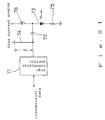
- Fig. 5 is a block diagram of a laser driving circuit according to an embodiment of a modulation method of a semiconductor laser.
- bias current I0 of a constant value (for example, 100mA) is formed by bias-current-forming circuit 21.
- a current-pulse-generating circuit 22 produces a modulation current ⁇ I of several mA, for example, at a timing corresponding to the transmission of data.
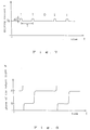
- An example of the waveform of the driving current I is shown in Fig. 7.
- the oscillation angular frequency ⁇ varies with the current change ⁇ I (as shown in Fig. 6), thereby producing a phase difference corresponding to a time integral of the change ⁇ .
- ⁇ I is determined to comply with an equation of time integration of ⁇ , namely, in the present embodiment as stated above, a relative phase difference of ⁇ can be produced before and after ⁇ I is applied.
- a variation of the phase ⁇ of the output light is shown in Fig. 8 in accordance with the waveform of the driving current of Fig. 7, with the same time position plotted on an abscissa having the same time scale as in Fig. 7. Namely, the phase ⁇ of the output light is inverted by ⁇ at a certain portion of the current variation ⁇ I, thereby showing that a phase modulation is enabled between 0 and ⁇ .
- the present embodiment by applying a small current variation ⁇ I to a constant bias current I0 the phase difference of ⁇ can be applied to the output light.
- the amplitude of the modulation current can be made extremely small, as described above, the load imposed on both the semiconductor laser and the driving circuit is extremely small.
- spreading of the oscillation wavelength is limited to sidebands caused by the modulation. It is suppressed to the same degree as when using an external modulator, thereby preventing the adverse effect of chirping.
- the present invention solves the big problem of limited high-speed operation with direct modulation, enabling high-speed modulation (for example, of several to several tens of Gb/s) which greatly exceeds the frequency limitation occurring with a direct modulation.
- the output light (phase-modulated light) of the semiconductor laser 23 obtained in the above embodiment is input to a self-homodyne-type optical interferometer as shown in Fig. 9.
- the optical interferometer 24 is constructed such that a light beam is divided or two light beams are combined by two half-mirrors 24a and 24b.
- a time delay is applied to light passing through one light path l2 via reflection at mirrors 24c and 24d, with respect to light passing through the other light path l1 .
- This time delay is equal to a single time band T (one time slot) of the driving current I as shown in Fig. 7.
- the output light from the optical interferometer 24 combines light of a certain time period obtained by the semiconductor laser 23 and light of a time period earlier or later by one unit, thereby providing a light pulse of "0" or"1" in accordance with a phase difference of ⁇ or 0 of the two combined lights.
- an output light (phase-modulated light) of the semiconductor laser 23 is intensity-modulated by a self-homodyne-type optical interferometer 24.
- the variation in intensity of the output lights from the optical interferometer 24 obtained in accordance with the phase variation of Fig. 8, is shown in Fig. 10.
- the intensity modulation of "0" and "1" can be applied to the output light from the semiconductor laser. Accordingly, in a similar manner to the first embodiment, the adverse effect of chirping is eliminated and load on the semiconductor laser and driving circuit is reduced, thereby realizing high-speed operation using direct modulation.
- the modulating current ⁇ I shown in Fig. 7 produces a phase difference of ⁇ but, as it may have a phase difference of - ⁇ , it may be modulated as shown in Fig. 11 such that ⁇ I is subtracted from I0.
- an intensity modulation similar to Fig. 10 can also be obtained if the output light from the laser is transmitted through the optical interferometer 24 of Fig. 9.
- the form of the modulation current ⁇ I need not be of ⁇ function or similar, but may be any type of function in which the integral becomes ⁇ /k in a narrow region in terms of time.
- an interferometer of the Michelson type shown in Fig. 12A
- one of the Fabry-Perot type shown in Fig. 12B
- optical interferometer 24e, 24f, and 24h represent mirrors
- 24g and 24i represent half mirrors.
- Fig. 13 shows a structure for realizing the first embodiment used as a method for stabilizing an optical interferometer according to the present invention, and the present embodiment is applied to the optical interferometer 24 shown in Fig. 9.
- An output light obtained by combining input lights at half mirror 24b as recited with reference to Fig. 9 can be detected by a photo detector 32 through a half mirror 31 as shown in Fig. 13.
- These two photo detectors 32 and 34 have relatively large time constants compared with the time interval used for phase modulation by semiconductor laser 23, and are constructed such that a large capacity is connected in parallel to an ordinary photodiode.
- an average intensity can be obtained by integrating the output light intensity in a time interval corresponding to a speed which is slower than that of the phase modulation (for example, about 1/100 sec with regard to a phase modulation of lGb/s). As described above, such variation of average intensity corresponds to the deviation of phase bias upon an intensity modulation.
- the oscillation wavelength of the semiconductor laser 23 is changed.
- the phase difference between the two lights to be combined at half mirror 24b varies, thereby changing the phase bias at the time of the intensity modulation and changing- the average intensity of the output light accordingly. Therefore, if a feedback is always applied so that the output of the differential amplifier 35 is made 0, the phase bias can be maintained at "1/2" thereby achieving a stabilized light output.
- the intensity of respective output lights detected by photo detectors 32 and 34 are reversed, the shift of the phase bias doubles, in the difference in respective light outputs, resulting in a large phase shift, thereby enabling extremely accurate detection of the deviation of respective light outputs.
- Fig. 14 shows a structure for realizing the second embodiment of a method for stabilizing an optical interferometer according to the present invention.
- a feedback is applied to a difference in light path to achieve stabilization of the interferometer.
- a mirror 24c of an optical interferometer 24 is secured to a piezo element 36. This element is driven in accordance with the output of differential amplifier 35 and mirror 24c is moved in the direction shown by the arrow, thereby changing the actual length of the light path from half mirror 24a to half mirror 24b through mirrors 24c and 24d.
- the phase difference of two lights to be combined by half mirror 24b can be changed.
- the phase bias can be maintained in an ideal condition in a similar manner to the above embodiment, thereby achieving a stabilized output.
- Fig. 15 shows a structure for realizing the third embodiment of a method for stabilizing an optical interferometer in accordance with the present invention.
- a heater 37 is provided on a light path between mirrors 24c and 24d in place of a piezo element 36 and the heater 37 is driven in accordance with the output of differential amplifier 35.
- a refractive index of the pertinent portion of the light path is changed, thereby varying the length of the light path accordingly.
- Fig. 16 shows a structure for realizing the fourth embodiment of the present invention, that is, a method of stabilizing an optical interferometer, and this embodiment is applied to an optical interferometer 10, as shown in Fig. 2
- two output lights having reversed light intensity are detected by photodetectors 32 and 34 through half mirrors 31 and 33 in a similar manner to the embodiment shown in Fig. 13.
- the differential amplifier 35 detects the difference in output from the photo detectors and, based on this difference, applies a feedback to an oscillation wavelength of semiconductor laser 38 which produces a constant light output.
- Fig. 17 shows a structure for realizing the fifth embodiment of a method for stabilizing an optical interferometer of the present invention. This is an example of an application to an optical interferometer 10′ in which two optical waveguides 2 and 3 in the optical interferometer 10 shown in Fig. 2 are made with the same length.
- a feedback is applied to the difference in optical waveguides 2 and 3, thereby changing the phase difference of the two lights output from the waveguides.
- the voltage applied to the electrode 6 varies in accordance with the output of the differential amplifier 35, thereby changing the length of the light path of the optical waveguide 3 using a variation in refractive index in accordance with the voltage applied to the electrode 6.
- the phase bias can be maintained in an ideal state like the respective embodiments explained hereinbefore, thereby achieving a stabilized output from optical interferometer 10′.
- the photo-detectors 32 and 34 and the differential amplifier 35 are used as a means for detecting the average intensity of the light output from the optical interferometers 24, 10, or 10′.
- the average intensity detecting means is not limited to this type, and any structure may be used, providing that an average intensity can be detected by integrating the intensity of the output light from an optical interferometer in a time interval corresponding to a speed which is slower than that of a phase modulation.
- the method of stabilizing an optical interferometer of the present invention can, of course, be applied to various optical interferometers, such as the Michelson or Fabry-Perot types, as well as the Mach-Zehnder type shown in Figs. 2 and 9.
- Figs. 4A and 4B Two kinds of dispositions are considered (or possible) as shown in Figs. 4A and 4B.
- Any structure in which a feedback is applied to a difference in length of optical light paths is suitable for both the dispositions shown in Figs. 4A and 4B, and any structure in which a feedback is applied to the oscillation wavelength as shown in Figs. 13 and 16, is suitable for the disposition shown in Fig. 4A.
- the disposition is advantageous in that the response time is fast.
- a feedback is applied to a difference in length of a light path in a disposition such as that shown in Fig. 4B, a direct light amplification is facilitated even when the light intensity is reduced on the way of transmission.
- Fig. 18 is a block diagram of the light modulation apparatus of the present invention and Fig. 19 shows a structure of the first embodiment thereof.
- the light modulator of the present embodiment comprises an AND circuit 50, a flip-flop 51, a condenser 52, a semiconductor laser 53, an optical isolator 54, a bias current source 55, an inductor 56, a resistor 57, an optical interferometer 58 (half mirrors 58a and 58b, and mirrors 58c and 58d), half mirrors 59, 60 and 61, photodetectors 62 and 63, a subtraction processing circuit 64 and a mirror driving portion 65.
- the circuit comprising the AND circuit 50 and the flip-flop 51 corresponds to the sign conversion portion 40
- the circuit comprising the condenser 52 and the resistor 57 corresponds to the differentiation circuit 41.
- the semiconductor laser 53, the optical interferometer 58 and the bias current source 55 correspond to the semiconductor laser 42, the optical interferometer 43 and the bias current source 44, respectively.
- transmission data comprising "1" and “0” is applied to the clock terminal CK of flip-flop 51.
- transmission data comprising "1" and “0”
- data appearing at the output terminal Q are reversed, and upon receiving transmission data "0", data appearing at output terminal Q remain unchanged. Therefore, a sign conversion is conducted so that the sign of the transmission data is converted, only when transmission data is "1", thereby enabling AND circuit 50 to produce an output in accordance with the transmission clock signal.
- the AND circuit 50 is provided to make the conversion output signal an RZ signal.
- This conversion output signal is supplied to semiconductor 53 as conversion current pulse ⁇ I through condenser 52 and is superimposed on a constant bias current I0 supplied from bias current source 55.
- This constant bias current I0 is determined to be a value such that semiconductor laser 53 performs a continuous laser oscillation to provide an output light of a desired intensity, as shown in Fig. 1.
- the output light from the semiconductor laser 53 is input to the optical interferometer 58 through a light isolator 54.
- the basic structure of the optical interferometer 58 is the same as that of the optical interferometer 24, shown, for example, in Fig. 9.
- a light is divided into two light signals, one of which propagates along a path including half mirrors 59 and 58b, and the other of which propagates along a path (a light delay circuit) including mirrors 58c and 58b and half mirrors 60 and 58b.
- a relative delay time is set equal to one time slot and a relative phase difference is set equal to 0 or ⁇ , and the optical interference of a self homodyne type is conducted.
- An optical fiber may be used for the light delay circuit instead of using mirrors 58c and 58b.
- Half mirrors 59, 60 and 61, photo detectors 62 and 63, a subtraction processing circuit 64 and a mirror driving portion 65 constitute one example of a structure for stabilizing an output from the optical interferometer 58 in a similar manner to the structure shown in Fig. 14.
- a differential amplifier for example, can be used for subtraction processing circuit 64, and a piezo element, for example, can be used for mirror driving portion 65.
- a product of a time integration of a modulation current pulse ⁇ I(t) applied to semiconductor laser 53 in a time interval corresponding to a time slot and chirping coefficient k is selected to be ⁇ or - ⁇ to satisfy the equation (1) in a similar manner to a modulation method for a semiconductor laser as shown in Fig. 5.
- a differentiation circuit comprising condenser 52, semiconductor laser 53 and resistor 57 is determined to provide a modulation current pulse ⁇ I(t) which satisfies the above-recited relationship and the output light from semiconductor laser 53 is modulated such that the phase ⁇ becomes ⁇ or - ⁇ .
- the relative delay time between one divided light signal and the other is set at one time slot and the relative phase difference at 0 or ⁇ in the optical interferometer 58. Therefore, when the relative phase difference is set at ⁇ and the phase ⁇ of the output light from the semiconductor laser 53 continues to be of the same value, the phase difference of the light signal applied to the half mirror 58b becomes ⁇ , thereby enabling the intensity of modulated output light to be "0". On the other hand, when the phase ⁇ of the output light from the semiconductor laser 53 is changed to ⁇ , the phase difference of the light signal applied to the half mirror 58b becomes 2 ⁇ for a period of one time slot, thereby enabling the relative value of the intensity of the modulation output light to become "1".
- a light intensity modulation can be conducted by superimposing a modulation current pulse ⁇ I(t) on a constant bias current I0 to drive semiconductor laser 53. This enables a phase ⁇ of the output light from semiconductor laser 53 to change to ⁇ or - ⁇ . The output light is thus applied to optical interferometer 58, thereby providing the light intensity modulation.
- the relative phase difference in the optical interferometer 58 is set at 0 and the phase ⁇ of the output light from the semiconductor laser 53 is changed to ⁇ , the phase difference becomes ⁇ for a period of one time slot and the intensity of the modulated output light becomes "0", and the relative value of the intensity of the modulated output light for the other time slot becomes "1".
- this conversion output signal is used for a modulating current pulse ⁇ I applied to the semiconductor laser 53
- the modulating current pulse ⁇ I is given the waveform shown in Fig. 20(c).
- the oscillation angular frequency ⁇ of semiconductor laser 53 is changed such that its phase ⁇ becomes ⁇ as recited above.
- differential circuit 41 (comprising condenser 52, and resister 57) differentiates the conversion output signal to provide a modulating current pulse as shown 10 in Fig. 20(d).
- the semiconductor laser 53 has the oscillation angular frequency ⁇ in accordance with the above modulating current pulse.
- the output light phase ⁇ from the semiconductor laser 53 corresponds to a time integration of an oscillation angular frequency ⁇ as recited above, and has the waveform shown in Fig. 20(e).
- the conversion output signal has a continuous "1”
- the semiconductor laser 53 can be driven to produce a change of ⁇ in the output light phase ⁇ .
- a light signal having this phase is incident to the half-mirror 58b. Therefore, the phase difference of the light signal which is incident to the half mirror 58, as shown in Fig. 20(f), is ⁇ when the conversion output signal is "0" , and 2 ⁇ (or 0 ) when it is "1".
- the light signals of the phase difference 2 ⁇ (or 0) interfere with each other at the half mirror 58b, thereby providing an output light which is intensity-modulated in accordance with the transmission data, as shown in Fig. 20(g).
- the bias current I0 supplied to the semiconductor laser 53 from bias current source 55 is determined in accordance with a characteristic of semiconductor laser 53.
- the bias current I0 may be, for example, 60 mA and the superimposed modulation current pulse ⁇ I supplied from the differential circuit may be, for example, 11 mA. Accordingly, as the modulating current pulse is small compared with the bias current, chirping does not occur, unlike in the prior art.
- the optical interferometer 58 provides a light delay before recombination of one time slot and determines the relative phase difference to be 0 or ⁇ . Thus, the loss in connection is small, and an extremely efficient intensity-modulation can be realized.
- Fig. 21 shows the circuit diagram of a differential circuit relating to the second embodiment of the light modulation apparatus of the present invention.
- the circuit in Fig. 21 comprises a sign conversion portion 71, a condenser 72, a semiconductor laser 73, a stub 74, a resistor 75 and an inductor 76.
- the sign conversion portion 71 converts the sign of the transmission data in a similar manner to that of the above embodiment, thereby producing a conversion output signal having a pulse width of 1/2 a time slot.
- the length l of the stub 74 is selected such that it reflects transmission data by reversing the polarity of the applied conversion output signal, thereby enabling the reversed conversion output signal to be supplied to the condenser 72 after 1/2 a time slot.
- the modulating current pulse supplied to the semiconductor laser 73 through the condenser 72 is formed with a waveform similar to that of Fig. 20(d) and the modulation current pulse is superimposed on the constant bias current supplied from the bias current source to be applied to the semiconductor laser 73. Therefore, the semiconductor laser 73 provides output light having a phase ⁇ as shown in Fig. 20(e).
- Fig. 22 is the third embodiment of a means for stabilizing the light modulator of the light modulation apparatus of the present invention.
- a feedback is applied to an oscillation wavelength of the semiconductor laser 53 by adding the output signal from the subtraction processing circuit 64 to the bias current source 55 in a similar manner to the stabilizing method shown in Fig. 13, thereby maintaining the output signal of the subtraction processing circuit 64 at 0.
- the phase bias upon intensity modulating the output from the optical interferometer 58 is maintained in an ideal state (as shown in Fig.3A), thereby stabilizing the output of the light interferometer 58.
- the above-recited light interferometer 58 is of the Mach-Zehnder-type and may be constructed of an optical waveguide. In place of the Mach-Zehnder-type light interferometer, one of the Michelson type or Fabry-Perot type may be used.
- the appearance probability of "1" and "0" for the transmission data is set at 1/2. If the appearance probability is set at a value other than 1/2, the subtraction processing circuit 64 processes the transmission data in accordance with this appearance probability so that a feedback can be applied to enable the difference between the detection signals from photo detectors 62 and 63 to have a predetermined value.
- the method of modulating the semiconductor laser, the method of stabilizing the optical interferometer and the light modulation apparatus are useful for light transmission systems shown in Figs. 4A and 4B and, may also be applied to various kinds of optical devices as a matter of course.
Landscapes
- Engineering & Computer Science (AREA)
- Computer Networks & Wireless Communication (AREA)
- Signal Processing (AREA)
- Physics & Mathematics (AREA)
- Electromagnetism (AREA)
- Optical Communication System (AREA)
- Semiconductor Lasers (AREA)
Claims (11)
- Halbleiterlaservorrichtung zum Aussenden eines optischen Signals, das in Übereinstimmung mit Übertragungsdaten moduliert ist, mita) einem Halbleiterlaser (11, 23, 38, 42, 53, 73) mit einem angelegten Vorstrom;b) Modulationsstrom-Erzeugungseinrichtungen (22, 40, 41, 50, 51, 52, 71, 72, 74) zum Erzeugen eines Treiberstromimpulses (I(t)), der an den Halbleiterlaser angelegt wird, um eine Phase von Ausgangslicht des Halbleiterlasers direkt zu modulieren; undc) Überlagerungseinrichtungen zum Überlagern des Treiberstroms mit dem Vorstrom;gekennzeichnet durch
d) Einrichtungen zum Bestimmen des Treiberstroms (I(t)) auf der Grundlage, daß ein Produkt eines Oszillationswellenlängen-Chirping-Koeffizienten (k) des Halbleiterlasers (11, 23, 38, 42, 53, 73) und eines Integrals des Treiberstromwertes während eines Zeitschlitzes der Übertragungsdaten, π oder -π ist. - Halbleiterlaservorrichtung nach Anspruch 1, dadurch gekennzeichnet, daß der Modulationsstromimpuls (I) entsprechend 1 oder 0 der Übertragungsdaten erzeugt wird.
- Halbleiterlaser nach Anspruch 1, dadurch gekennzeichnet, daß der Modulationsstromimpuls (I) von einem δ-Funktionstyp ist.
- Halbleiterlaservorrichtung nach Anspruch 2, gekennzeichnet durch einen Erfassungsschaltkreis (12, 24, 43, 58) vom selbst-homodynen Typ, um eine Intensitätsmodulation zum Umwandeln des phasenmodulierten Ausgangslichts von dem Halbleiterlaser in einen Lichtimpuls vorzusehen.
- Halbleiterlaservorrichtung nach Anspruch 4, dadurch gekennzeichnet, daß der selbst-homodyne Erfassungsschaltkreis einen Interferometerschaltkreis vom Mach-Zehnder-Typ oder einen Interferometerschaltkreis vom Michelson-Typ umfaßt, um eine Differenz von einem Zeitschlitz bereitzustellen, welche durch eine Verzögerung oder einen Interferometerschaltkreis vom Fabry-Perot-Typ bewirkt wird.
- Halbleiterlaservorrichtung nach Anspruch 1, dadurch gekennzeichnet, daß das Ausgangslicht vom Halbleiterlaser (11, 23, 38, 42, 53, 73), welches der Phasenmodulation unterzogen ist, an eine optische Faser (13) zur Übertragung angelegt wird, und das Ausgangslicht in einen Lichtimpuls von 0 oder 1 am Ausgangsanschluß der optischen Übertragungsfaser mittels eines selbst-homodynen Erfassungsschaltkreises umgewandelt wird.
- Halbleiterlaservorrichtung nach Anspruch 1, gekennzeichnet durch einen Lichtinterferenzschaltkreis (12, 24, 43, 58) zum Teilen des Eingangslichts, um zu ermöglichen, daß das geteilte Eingangslicht durch zwei Lichtpfade (l₁, l₂) läuft, welche verschiedene Lichtpfadlängen haben, und zum Kombinieren des geteilten Eingangslichts danach, um ein intensitätsmoduliertes Ausgangslicht auf der Grundlage der Phasendifferenz zwischen den zwei zu kombinierenden Lichtern vorzusehen, worin eine Rückkopplung an eine Lichtwellenlänge des Eingangslichts unter Verwendung einer durchschnittlichen Intensität angelegt wird, die erhalten wird durch Integrieren der Intensität des Ausgangslichts von dem Lichtinterferenzschaltkreis (12, 24, 43, 58) in einem Zeitintervall entsprechend einer Geschwindigkeit, welche langsamer ist als die der Phasenmodulation, wodurch die Phasenvoreinstellung zur Zeit der Intensitätsmodulation korrigiert wird.
- Halbleiterlaservorrichtung nach Anspruch 1, gekennzeichnet durch einen optischen Interferenzschaltkreis, wobei der optische Interferenzschaltkreis (12, 24, 43, 58) Einrichtungen zum Empfangen eines Eingangslichts umfaßt, welches ein phasenmoduliertes Lichtsignal umfaßt, das von dem Ausgangslicht von dem Halbleiterlaser (11, 23, 38, 42,53, 73) erhalten wird, Einrichtungen (24b) zum Kombinieren eines geteilten Signals, welches erhalten wird durch Teilen des Eingangslichts, und welches entlang zweier optischer Pfade (l₁, l₂) läuft, welche verschiedene optische Pfadlängen haben, und Einrichtungen zum Vorsehen eines Ausgangslichts, welches einer Intensitätsmodulation auf der Grundlage der Phasendifferenz zwischen den zwei zu kombinierenden Lichtern unterzogen ist, worin eine Rückkopplung auf die Differenz in optischen Pfadlängen der zwei optischen Pfade (l₁, l₂) angelegt wird durch Verwendung einer durchschnittlichen Lichtintensität, die durch Integrieren der Intensität des Ausgangssignallichtes von dem optischen Interferenzschaltkreis (12, 24, 43, 58) in einem Zeitintervall erhalten wird, das einer Geschwindigkeit entspricht, welche langsamer ist als die der Modulation, und worin eine Phasenvoreinstellung während der Intensitätsmodulation korrigiert wird.
- Halbleiterlaservorrichtung nach Anspruch 1, gekennzeichnet durch einen Treiberschaltkreis (21, 22) mit Einrichtungen (40, 51, 71) zum Umwandeln eines Vorzeichens der Übertragungsdaten nur, wenn die Übertragungsdaten entweder 1 oder 0 umfassen, einen Differenzierungsschaltkreis (41, 52, 72, 74) zum Differenzieren eines Umwandlungsausgangssignals von der Vorzeichenumwandlungseinrichtung (40, 51, 71), und Treibereinrichtungen zum Überlagern des differenzierten Ausgangssignals von dem Differenzierungsschaltkreis auf einen konstanten Vorstrom als ein Modulationsimpulsstrom.
- Halbleiterlaservorrichtung nach Anspruch 9, gekennzeichnet durch ein selbst-homodynes Interferometer mit einem optischen Verzögerungsschaltkreis (58b, 58c, 65), um die relative Phasendifferenz zwischen einem und anderen der geteilten Lichter zu 0 oder π zu machen, wobei die geteilten Lichter erhalten werden durch Teilen des Ausgangslichts von dem Halbleiterlaser (53) und dadurch, daß die relative Verzögerung ein Zeitschlitz ist.
- Halbleiterlaservorrichtung nach Anspruch 9, dadurch gekennzeichnet, daß der Differenzierungsschaltkreis mit einer Stichleitung (74) ausgestattet ist.
Applications Claiming Priority (7)
| Application Number | Priority Date | Filing Date | Title |
|---|---|---|---|
| JP49803/88 | 1988-03-04 | ||
| JP4980388 | 1988-03-04 | ||
| JP18539988 | 1988-07-27 | ||
| JP185399/88 | 1988-07-27 | ||
| JP20816388 | 1988-08-24 | ||
| JP208163/88 | 1988-08-24 | ||
| PCT/JP1989/000220 WO1989008356A1 (en) | 1988-03-04 | 1989-03-02 | Method and apparatus for modulating a semiconductor laser |
Publications (3)
| Publication Number | Publication Date |
|---|---|
| EP0357799A1 EP0357799A1 (de) | 1990-03-14 |
| EP0357799A4 EP0357799A4 (en) | 1992-05-13 |
| EP0357799B1 true EP0357799B1 (de) | 1995-11-08 |
Family
ID=27293745
Family Applications (1)
| Application Number | Title | Priority Date | Filing Date |
|---|---|---|---|
| EP89903271A Expired - Lifetime EP0357799B1 (de) | 1988-03-04 | 1989-03-02 | Vorrichtung und verfahren zur modulierung eines halbleiterlasers |
Country Status (4)
| Country | Link |
|---|---|
| US (1) | US5073331A (de) |
| EP (1) | EP0357799B1 (de) |
| DE (1) | DE68924747T2 (de) |
| WO (1) | WO1989008356A1 (de) |
Families Citing this family (24)
| Publication number | Priority date | Publication date | Assignee | Title |
|---|---|---|---|---|
| JP2758211B2 (ja) * | 1989-06-19 | 1998-05-28 | 富士通株式会社 | 周波数直接変調psk方式 |
| US5255274A (en) * | 1989-09-06 | 1993-10-19 | The Board Of Trustees Of The Leland Stanford University | Broadband laser source |
| JP2917333B2 (ja) * | 1989-11-30 | 1999-07-12 | 日本電気株式会社 | 光送信方法及び光送信装置 |
| JPH0478235A (ja) * | 1990-07-18 | 1992-03-12 | Fujitsu Ltd | 直接変調psk伝送システム並びに該システムにおける自動周波数制御方法、復調方法及び位相雑音抑圧方法 |
| JP3001943B2 (ja) * | 1990-08-30 | 2000-01-24 | 株式会社東芝 | 偏波スイッチング光源、光受信装置及びコヒーレント光伝送システム |
| JP2970776B2 (ja) * | 1990-12-17 | 1999-11-02 | 富士通株式会社 | 光送信装置 |
| US5170403A (en) * | 1991-05-31 | 1992-12-08 | Digital Equipment Corporation | Modulation circuit for grayscale laser printing |
| JP3223562B2 (ja) * | 1992-04-07 | 2001-10-29 | 株式会社日立製作所 | 光送信装置、光伝送装置および光変調器 |
| US5208817A (en) * | 1992-04-10 | 1993-05-04 | At&T Bell Laboratories | Modulator-based lightwave transmitter |
| DE19801469C2 (de) | 1998-01-16 | 2001-05-17 | Campus Technologies Ag Zug | Vorrichtung zur Erfassung oder Erzeugung optischer Signale |
| US6441940B1 (en) * | 1998-10-09 | 2002-08-27 | Agere Systems Guardian Corp. | Wavelength stabilization of light emitting components |
| US6317526B1 (en) * | 1998-12-21 | 2001-11-13 | Fujitsu Limited | Optical phase controller and optical switch |
| US6618404B2 (en) * | 2001-06-19 | 2003-09-09 | Lockheed Martin Corporation | Method for producing highly accurate frequency and FM of a laser |
| WO2003061160A1 (fr) * | 2002-01-09 | 2003-07-24 | Advantest Corporation | Circuit de modulation de phase, appareil d'essai, et systeme de communication |
| US7747171B1 (en) | 2002-09-10 | 2010-06-29 | Meriton Networks Us Inc. | Method and apparatus for alleviating slope-induced impairments to chirped optical signals propagating in an optical transmission system |
| US20060268277A1 (en) * | 2005-02-23 | 2006-11-30 | Optoplex Corporation | Michelson interferometer based delay line interferometers |
| KR100701101B1 (ko) * | 2004-12-20 | 2007-03-28 | 한국전자통신연구원 | 광 간섭계 제어 장치 및 그 방법 |
| EP1694017B1 (de) * | 2005-02-18 | 2013-11-27 | Nokia Solutions and Networks GmbH & Co. KG | Verfahren und Vorrichtung zur Demodulation eines optischen DPSK-Signales |
| US20090214224A1 (en) * | 2007-04-03 | 2009-08-27 | Celight, Inc. | Method and apparatus for coherent analog rf photonic transmission |
| US7782913B2 (en) * | 2007-07-20 | 2010-08-24 | Corning Incorporated | Intensity modulation in wavelength converting optical package |
| WO2009114163A2 (en) * | 2008-03-11 | 2009-09-17 | Oewaves, Inc. | Optical locking based on optical resonators with high quality factors |
| JP2009253598A (ja) * | 2008-04-04 | 2009-10-29 | Fujitsu Ltd | 位相変調信号受信装置 |
| US8781336B1 (en) * | 2011-02-10 | 2014-07-15 | Finisar Corporation | Optical filter for use in a laser transmitter |
| US10747031B2 (en) | 2018-08-07 | 2020-08-18 | Teraxion Inc. | Method and system for optical phase modulation with reduced harmonic content |
Citations (1)
| Publication number | Priority date | Publication date | Assignee | Title |
|---|---|---|---|---|
| GB2144598A (en) * | 1981-07-14 | 1985-03-06 | British Telecomm | Laser telecommunications system |
Family Cites Families (7)
| Publication number | Priority date | Publication date | Assignee | Title |
|---|---|---|---|---|
| JPS57112158A (en) * | 1980-12-29 | 1982-07-13 | Fujitsu Ltd | Code converting circuit |
| JPS5943724A (ja) * | 1982-09-02 | 1984-03-10 | Tokyo Erekutoron Kk | 超音波浮上型搬送装置 |
| JPS60235543A (ja) * | 1984-05-08 | 1985-11-22 | Nec Corp | 光位相変調方法 |
| JPS61212932A (ja) * | 1985-03-18 | 1986-09-20 | Nec Corp | 位相偏移変調光送信装置 |
| JPS62189832A (ja) * | 1986-02-17 | 1987-08-19 | Nec Corp | 光送信装置 |
| NL8601510A (nl) * | 1986-06-11 | 1988-01-04 | Philips Nv | Inrichting voor het aansturen van een laser. |
| NL8602303A (nl) * | 1986-09-12 | 1988-04-05 | Philips Nv | Werkwijze voor het in pulsmode aansturen van een halfgeleiderlaser, aanstuurinrichting voor een halfgeleiderlaser en laserschrijfapparaat voorzien van een dergelijke aanstuurinrichting. |
-
1989
- 1989-03-02 DE DE68924747T patent/DE68924747T2/de not_active Expired - Fee Related
- 1989-03-02 WO PCT/JP1989/000220 patent/WO1989008356A1/ja active IP Right Grant
- 1989-03-02 EP EP89903271A patent/EP0357799B1/de not_active Expired - Lifetime
- 1989-03-02 US US07/340,010 patent/US5073331A/en not_active Expired - Lifetime
Patent Citations (1)
| Publication number | Priority date | Publication date | Assignee | Title |
|---|---|---|---|---|
| GB2144598A (en) * | 1981-07-14 | 1985-03-06 | British Telecomm | Laser telecommunications system |
Also Published As
| Publication number | Publication date |
|---|---|
| EP0357799A4 (en) | 1992-05-13 |
| DE68924747D1 (de) | 1995-12-14 |
| US5073331A (en) | 1991-12-17 |
| EP0357799A1 (de) | 1990-03-14 |
| DE68924747T2 (de) | 1996-05-02 |
| WO1989008356A1 (en) | 1989-09-08 |
Similar Documents
| Publication | Publication Date | Title |
|---|---|---|
| EP0357799B1 (de) | Vorrichtung und verfahren zur modulierung eines halbleiterlasers | |
| EP0444688B1 (de) | Optischer Sender | |
| EP0235662B1 (de) | Optischer Sender mit einem optischen Frequenzdiskriminator | |
| US4561119A (en) | Optical frequency modulation system | |
| US7215894B2 (en) | Optical transmitter device | |
| JPH04192729A (ja) | 光送信装置 | |
| JPH10123471A (ja) | 光送信機 | |
| US6317249B1 (en) | Optical modulator outputting an optical signal with a drive voltage signal dependent upon an input signal | |
| JP3210061B2 (ja) | 光干渉器の動作点安定化装置 | |
| EP0431474B1 (de) | Optischer Faserkreisel | |
| US20030044108A1 (en) | Polarization mode dispersion compensation using a wavelength locked loop | |
| WO1992004597A1 (fr) | Appareil de mesure de la vitesse angulaire par interference optique | |
| JP3538619B2 (ja) | 光変調器の特性評価方法、およびそれを用いた高周波発振装置の制御方法 | |
| US11852948B2 (en) | Optical transmitter, optical transceiver, and method of controlling bias voltage of electro-optic modulator | |
| US20050053385A1 (en) | Optical apparatus and optical processing method | |
| USRE36088E (en) | Optical transmitter | |
| JP2760856B2 (ja) | マッハツェンダ型光変調器を用いた位相シフトキーイング方式 | |
| US4979825A (en) | Device for measuring optical frequency modulation characteristics | |
| EP0194096B1 (de) | C3(Cleaved-Coupled-Cavity)-Laser zur Ausführung eines Systems für Messung schwacher Signale | |
| JPH05232412A (ja) | LiNbO3 マッハツェンダ干渉型変調器の制御装置 | |
| JPS60147716A (ja) | 消光比制御光送信装置 | |
| JP3207211B2 (ja) | 半導体レーザの光周波数偏移量の測定,制御装置 | |
| JP3065423B2 (ja) | レーザダイオードの駆動装置 | |
| JP4316212B2 (ja) | 光強度変調装置 | |
| JPS61212932A (ja) | 位相偏移変調光送信装置 |
Legal Events
| Date | Code | Title | Description |
|---|---|---|---|
| PUAI | Public reference made under article 153(3) epc to a published international application that has entered the european phase |
Free format text: ORIGINAL CODE: 0009012 |
|
| 17P | Request for examination filed |
Effective date: 19891024 |
|
| AK | Designated contracting states |
Kind code of ref document: A1 Designated state(s): DE FR GB NL |
|
| A4 | Supplementary search report drawn up and despatched |
Effective date: 19920326 |
|
| AK | Designated contracting states |
Kind code of ref document: A4 Designated state(s): DE FR GB NL |
|
| 17Q | First examination report despatched |
Effective date: 19930806 |
|
| GRAA | (expected) grant |
Free format text: ORIGINAL CODE: 0009210 |
|
| AK | Designated contracting states |
Kind code of ref document: B1 Designated state(s): DE FR GB NL |
|
| REF | Corresponds to: |
Ref document number: 68924747 Country of ref document: DE Date of ref document: 19951214 |
|
| ET | Fr: translation filed | ||
| PLBE | No opposition filed within time limit |
Free format text: ORIGINAL CODE: 0009261 |
|
| STAA | Information on the status of an ep patent application or granted ep patent |
Free format text: STATUS: NO OPPOSITION FILED WITHIN TIME LIMIT |
|
| 26N | No opposition filed | ||
| REG | Reference to a national code |
Ref country code: GB Ref legal event code: IF02 |
|
| PGFP | Annual fee paid to national office [announced via postgrant information from national office to epo] |
Ref country code: GB Payment date: 20040225 Year of fee payment: 16 |
|
| PGFP | Annual fee paid to national office [announced via postgrant information from national office to epo] |
Ref country code: FR Payment date: 20040309 Year of fee payment: 16 |
|
| PGFP | Annual fee paid to national office [announced via postgrant information from national office to epo] |
Ref country code: NL Payment date: 20040310 Year of fee payment: 16 |
|
| PGFP | Annual fee paid to national office [announced via postgrant information from national office to epo] |
Ref country code: DE Payment date: 20040311 Year of fee payment: 16 |
|
| PG25 | Lapsed in a contracting state [announced via postgrant information from national office to epo] |
Ref country code: GB Free format text: LAPSE BECAUSE OF NON-PAYMENT OF DUE FEES Effective date: 20050302 |
|
| PG25 | Lapsed in a contracting state [announced via postgrant information from national office to epo] |
Ref country code: NL Free format text: LAPSE BECAUSE OF NON-PAYMENT OF DUE FEES Effective date: 20051001 Ref country code: DE Free format text: LAPSE BECAUSE OF NON-PAYMENT OF DUE FEES Effective date: 20051001 |
|
| GBPC | Gb: european patent ceased through non-payment of renewal fee |
Effective date: 20050302 |
|
| PG25 | Lapsed in a contracting state [announced via postgrant information from national office to epo] |
Ref country code: FR Free format text: LAPSE BECAUSE OF NON-PAYMENT OF DUE FEES Effective date: 20051130 |
|
| NLV4 | Nl: lapsed or anulled due to non-payment of the annual fee |
Effective date: 20051001 |
|
| REG | Reference to a national code |
Ref country code: FR Ref legal event code: ST Effective date: 20051130 |