EP0356967B1 - Pin electronics device having a phase adjustment function for IC testers and phase adjustment method therefor - Google Patents
Pin electronics device having a phase adjustment function for IC testers and phase adjustment method therefor Download PDFInfo
- Publication number
- EP0356967B1 EP0356967B1 EP89115860A EP89115860A EP0356967B1 EP 0356967 B1 EP0356967 B1 EP 0356967B1 EP 89115860 A EP89115860 A EP 89115860A EP 89115860 A EP89115860 A EP 89115860A EP 0356967 B1 EP0356967 B1 EP 0356967B1
- Authority
- EP
- European Patent Office
- Prior art keywords
- terminal
- strobe
- logic level
- pulse
- input
- Prior art date
- Legal status (The legal status is an assumption and is not a legal conclusion. Google has not performed a legal analysis and makes no representation as to the accuracy of the status listed.)
- Expired - Lifetime
Links
Images

Classifications
-
- G—PHYSICS
- G01—MEASURING; TESTING
- G01R—MEASURING ELECTRIC VARIABLES; MEASURING MAGNETIC VARIABLES
- G01R31/00—Arrangements for testing electric properties; Arrangements for locating electric faults; Arrangements for electrical testing characterised by what is being tested not provided for elsewhere
- G01R31/28—Testing of electronic circuits, e.g. by signal tracer
- G01R31/317—Testing of digital circuits
- G01R31/3181—Functional testing
- G01R31/319—Tester hardware, i.e. output processing circuits
- G01R31/31903—Tester hardware, i.e. output processing circuits tester configuration
- G01R31/31908—Tester set-up, e.g. configuring the tester to the device under test [DUT], down loading test patterns
- G01R31/3191—Calibration
Definitions
- the present invention relates to a phase adjustable pin electronics device for use in IC testers and a phase adjustment method therefor.
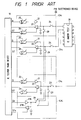
- Fig. 1 shows the arrangement of a conventional IC tester as disclosed in U.S. Patent No. 4,497,056.
- Reference numeral 10 indicates generally an IC tester main device, 20 a pin electronics device, and 30 an IC under test.
- the pin electronics device 20 is provided with drivers 21 each providing a test pattern signal for each of channels CH1 to CH n corresponding to respective terminals of the IC under test 30, and logical comparators 22 each determining whether or not a response out put signal from one of the terminals of the IC under test 30 has a predetermined level at predetermined timing.
- the driver 21 and the logical comparator 22 for each channel are connected via a relay 24 to the corresponding terminal of the IC under test 30.
- Reference numerals 25 and 26 designate variable delay elements for skew adjustment in each channel.
- the variable delay elements 25 and 26 are provided in each channel for adjusting the phase of a drive pulse D to be applied to the corresponding terminal of the IC under test 30 and the phase of a strobe pulse ST to be applied to the logical comparator 22, thereby putting the phases (hereinafter referred to as skews) of the drive pulses D and the skews of the strobe pulses ST into agreement.
- the logical comparators 22 each compare the input signal level with a reference voltage at the fall of the strobe pulse ST, and output and hold a logical "1" or "0" until the next comparison is effected depending upon whether the former is higher or lower than the latter.
- the pin electronics device 20 further includes a calibrator CAL which has a reference driver 27A and a reference logical comparator 27B which perform a reference operation with respect to the driver 21 and the logical comparator 22 provided for each channel.
- the reference driver 27A and the reference logical comparator 27B are used to adjust the variable delay elements 25 and 26 in such a manner as described below.
- All the relays 24 are turned OFF and all calibration relays 29 ON, and the driver 21 of a desired channel to be adjusted is selected by a select switch 28.
- the drive pulse D supplied from the selected driver 21 via the calibration relay and the select switch 28 is strobed by a reference strobe pulse ST R at the reference logical comparator 27B, and the delay amount of the variable delay element 25 in the selected channel is adjusted so as to bring the phase of the drive pulse into a fixed relation to the reference strobe pulse. That is, by gradually changing the delay amount of the variable delay element 25 and fixing it a at a value where the output logic of the reference logical comparator 27B reverses, the reference strobe pulse ST R which is applied to the reference logical comparator 27B is positioned at the edge of the drive pulse D which is output from the driver 21 in the selected channel. By this adjustment the skew of the driver 21 is set to a reference value. The skew adjustment for the drivers 21 of the other channels also similarly takes place after changing over the select switch 28 each time.
- the reference driver 27A outputs a reference drive pulse D R of a reference phase
- the reference drive pulse D R is supplied to and strobed by the logical comparator 22 of the channel selected by the select switch 28, and the delay amount of the variable delay element 26 is adjusted to a value where the output logic of the logical comparator 22 reverses, whereby the strobe pulse D is positioned at the edge of the reference drive pulse D R .
- the skews of the logical comparators 22 of the other channels are adjusted by similarly adjusting the delay amounts of the delay elements 26.
- the prior art performs the skew adjustment for the drivers 21 and the logical comparators 22 provided in the respective channels CH1 through CH n .
- the numbers of drivers 21 and the logical comparators 22 are very large, because they are provided corresponding to respective terminals of the IC under test 30. Consequently, it takes much time to adjust the drivers 21 and the logical comparators 22 one by one.
- the additional provision of the select switch 28 and the calibration relays 29 inevitably increases the physical size of the device.
- the electrostatic capacitance of the calibration relay 29 degrades the signal waveform which is provided to the IC under test 30 and the waveform of a response signal which is input into the logical comparator 22 from the IC under test 30.
- the line length from the connecting point between each calibration relay 29 and a corresponding channel to the select switch 28 differs with the channels, an error is produced even if the skew adjustment is made.
- Another object of the present invention is to provide a phase adjustment method for such device.
- an OR gate is provided in association with the logical comparator of each channel corresponding to one of respective terminals of an IC under test and a reference strobe pulse of a reference phase is applied via such OR gates to all the logical comparators at the same time.
- each driver provides a drive pulse and its phase is adjusted by adjusting a variable delay element connected to the driver system so that the edge of the drive pulse may agree with the position of the reference strobe pulse.
- each logical comparator adjusts a variable delay element inserted in the strobe pulse supply line so that the position of the strobe pulse may agree with the edge of the drive pulse.
- the phase of the strobe pulse in each logical comparator is put into agreement with the phase of the drive pulse, and as a result, the skews of the strobe pulses of the respective channels are made equal to one another.
- a reference strobe pulse of a reference phase is prepared for the logical comparator of each channel corresponding to one of the terminals of the IC under test, and the skew adjustment of the driver can be effected through use of the reference strobe pulse and the logical comparator. Since this skew adjustment can be performed for all the channels at one time, the adjustment can be achieved in a short time.
- the skew of the strobe pulse which is applied to the logical comparator can be adjusted utilizing the drive pulse which is yielded from the skew-adjusted driver.
- This skew adjustment of the strobe pulse can also be achieved for all the channels at the same time. Hence this skew adjustment can also be performed in a short time.
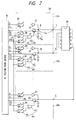
- Fig. 2 illustrates in block form an embodiment of the present invention.
- the same reference numerals are used as those in connection with Fig. 1, where the components are the same.
- the reference strobe pulse supply path 40 comprises an OR gate 42 provided in association with the logical comparator 22 and a variable delay element 43 connected between the OR gate 42 and a strobe pulse output terminal 41 of the IC tester main device 10.
- the amount of delay of the reference strobe pulse which occurs in the path from the strobe pulse output terminal 41 to a strobe terminal A of the logical comparator 22 through the reference strobe pulse supply path 40 in each channel, is preset to a value T CAL .
- T CP is the amount of delay (commonly referred to as a set-up time) between the connection point B of the driver 21 and the logical comparator 22 and the strobe pulse input terminal A of the logical comparator 22.
- T CP is the amount of delay (commonly referred to as a set-up time) between
- the above-mentioned adjustment is to ensure that the timing t c of logical comparison by the logical comparator 22 in each channel, for which its set-up time T CP has been compensated for, is set to the same position for all the channels relative to the output timing t1 of the reference strobe pulse ST R at the reference strobe output terminal 41 shown in Fig. 3A.
- the reference strobe pulse ST R at the terminal 41 shown in Fig. 3A arrives at the strobe input terminal A of the logical comparator 22 after the delay time T CAL as shown in Fig.
- the logical comparator 22 performs the logical comparison of a signal applied to its input terminal B (the connection point B).
- the signal to the input terminal B is delayed for the set-up time T CP owing to the internal delay (i.e. the set-up time) of the logical comparator 22 before it is subjected to the level determination, (i.e. logical comparation)
- the logical comparison at the fall of the strobe pulse at the time t1 means that the level of the signal which is applied to the input terminal B is determined at the time t c earlier than the time t1 by the set-up time T CP as depicted in Figs. 3B and 3C.
- T CL - T C K constant in the course of manufacture as mentioned previously means that the logical comparators 22 in the channels CH1 through CH n all perform the level determination at the same time point t c with respect to the reference strobe pulse ST R .
- a driver pulse D is applied to each driver 21 and a reference strobe pulse ST R is provided to the strobe pulse output terminal 41.
- the delay amount of the variable delay element 25 is adjusted so that the reference strobe pulse ST R falls at an edge of the drive pulse in the logical comparator 22. That is to say, the IC tester main device 10 always monitors the output logic of the logical comparator 22 and yields a control signal C1 which causes an increase (or decrease) in the delay amount of the variable delay element 25 until the output logic of the logical comparator 22 reverses.
- Fig. 3C shows the waveform of the drive pulse D adjusted in its delay so that the logical comparator output reverses at the fall of the reference strobe pulse ST R at the time t1 as shown in Figs.
- the delay amount of the variable delay element 26 is adjusted so that the fall of the strobe pulse ST may coincide with the edge of the drive pulse D. This adjustment is also conducted by a control signal C2 which is provided from the IC tester main body 10 as in the case of the afore-mentioned adjustment of the variable delay element 25.
- the skew adjustment of the strobe pulse ST which is applied to the logical comparator 22 in each channel terminates with this adjustment.
- Fig. 4 illustrates a modified form of the principal part of the present invention, in which two logical comparators 22A and 22B are provided for each channel.
- the variable delay elements 43, 25 and 26 are adjusted in the same manner as described previously with regard to Fig. 2.
- the IC tester main device 10 outputs a continuous "1" level to the output terminal 41 and the logical comparator 22A makes a level comparison of its input signal at all times and outputs the result of comparison as it is.
- the logical comparator 22A of the preceding stage operates as an ordinary level comparator which has no hold function
- the logical comparator 22B of the succeeding stage operates as a latch which holds the result of logical comparison from the preceding stage at the strobe timing.
- the OR gates 42 in Fig. 2 can be left out and the elements that are disposed as close to the input/output terminals C as possible can be limited to the drivers 21 and the logical comparators 22A.
- the number of elements to be disposed in close proximity to the input/output terminal C of each channel is three, i.e. the driver 21, the logical comparator 22 and the OR gate 42, but in the embodiment shown in Fig. 4 the number of such elements can be reduced to two, i.e. the driver 21 and the logical comparator 22A.
- the structure of the modified form depicted in Fig. 4 permits the reduction of the number of elements to be disposed near the input/output terminals C as mentioned above, and hence affords a margin of space accordingly; so that the number of channels can be increased in accordance with an increase in the number of terminals of the IC under test 30.
- the present invention adopts an arrangement in which no calibration switch is connected to the connection point B of the driver 21 and the logical comparator 22, and this eliminates the possibility of degrading the waveforms of the drive pulse which is applied to the IC under test 30 from the drive 21 and the response signal which is applied to the logical comparator 22 from the IC under test 30. Hence the IC under test 30 can be tested correctly.
- the time necessary for the skew adjustment can be reduced to 1/n (where n is the number of terminals of the IC under test 30) as compared with the time needed in the prior art. This affords reduction of the time for test and permits efficient testing of IC's.
- the present invention is therefore of great utility in practical use.
Landscapes
- Engineering & Computer Science (AREA)
- General Engineering & Computer Science (AREA)
- Physics & Mathematics (AREA)
- General Physics & Mathematics (AREA)
- Tests Of Electronic Circuits (AREA)
Applications Claiming Priority (2)
| Application Number | Priority Date | Filing Date | Title |
|---|---|---|---|
| JP63215855A JP2688941B2 (ja) | 1988-08-29 | 1988-08-29 | 位相補正装置 |
| JP215855/88 | 1988-08-29 |
Publications (3)
| Publication Number | Publication Date |
|---|---|
| EP0356967A2 EP0356967A2 (en) | 1990-03-07 |
| EP0356967A3 EP0356967A3 (en) | 1991-07-03 |
| EP0356967B1 true EP0356967B1 (en) | 1995-11-08 |
Family
ID=16679392
Family Applications (1)
| Application Number | Title | Priority Date | Filing Date |
|---|---|---|---|
| EP89115860A Expired - Lifetime EP0356967B1 (en) | 1988-08-29 | 1989-08-28 | Pin electronics device having a phase adjustment function for IC testers and phase adjustment method therefor |
Country Status (4)
| Country | Link |
|---|---|
| US (1) | US4929888A (ja) |
| EP (1) | EP0356967B1 (ja) |
| JP (1) | JP2688941B2 (ja) |
| DE (1) | DE68924744T2 (ja) |
Families Citing this family (46)
| Publication number | Priority date | Publication date | Assignee | Title |
|---|---|---|---|---|
| US5025205A (en) * | 1989-06-22 | 1991-06-18 | Texas Instruments Incorporated | Reconfigurable architecture for logic test system |
| US5235566A (en) * | 1989-09-07 | 1993-08-10 | Amdahl Corporation | Clock skew measurement technique |
| US5003256A (en) * | 1989-09-07 | 1991-03-26 | Amdahl Corporation | Clock skew measurement technique |
| JP2582906B2 (ja) * | 1989-10-21 | 1997-02-19 | 東芝マイクロエレクトロニクス株式会社 | 半導体装置の直流電流・電圧特性の測定方法 |
| US5293626A (en) * | 1990-06-08 | 1994-03-08 | Cray Research, Inc. | Clock distribution apparatus and processes particularly useful in multiprocessor systems |
| JPH0481675A (ja) * | 1990-07-25 | 1992-03-16 | Mitsubishi Electric Corp | 半導体デバイステスト装置 |
| US5212443A (en) * | 1990-09-05 | 1993-05-18 | Schlumberger Technologies, Inc. | Event sequencer for automatic test equipment |
| US5225772A (en) * | 1990-09-05 | 1993-07-06 | Schlumberger Technologies, Inc. | Automatic test equipment system using pin slice architecture |
| US5471136A (en) * | 1991-07-24 | 1995-11-28 | Genrad Limited | Test system for calculating the propagation delays in signal paths leading to a plurality of pins associated with a circuit |
| FR2682191B1 (fr) * | 1991-10-04 | 1995-08-11 | Aerospatiale | Methode de compensation automatique des incertitudes de temps d'un systeme electronique teste par un testeur automatique. |
| US5268639A (en) * | 1992-06-05 | 1993-12-07 | Rambus, Inc. | Testing timing parameters of high speed integrated circuit devices |
| US5402079A (en) * | 1992-12-18 | 1995-03-28 | Vlsi Technology, Inc. | Integrated circuit relay control system |
| JP3591657B2 (ja) * | 1993-10-13 | 2004-11-24 | 株式会社アドバンテスト | 半導体ic試験装置 |
| US5459738A (en) * | 1994-01-26 | 1995-10-17 | Watari; Hiromichi | Apparatus and method for digital circuit testing |
| JPH07294605A (ja) * | 1994-04-22 | 1995-11-10 | Advantest Corp | 半導体試験装置用校正データの転送装置及びその方法 |
| US5521493A (en) * | 1994-11-21 | 1996-05-28 | Megatest Corporation | Semiconductor test system including a novel driver/load circuit |
| US5589766A (en) * | 1995-04-06 | 1996-12-31 | General Electric Company | Field-testable integrated circuit and method of testing |
| JPH07244122A (ja) * | 1995-08-31 | 1995-09-19 | Advantest Corp | 半導体試験装置用遅延補正回路 |
| JPH09318704A (ja) * | 1996-05-30 | 1997-12-12 | Ando Electric Co Ltd | Ic試験装置 |
| KR100245929B1 (ko) * | 1997-06-30 | 2000-03-02 | 윤종용 | 클록 사용 제한조건이 설정된 고속 메모리 소자 검사방법 |
| US6820234B2 (en) | 1998-06-29 | 2004-11-16 | Acuid Limited | Skew calibration means and a method of skew calibration |
| AU9654198A (en) | 1998-06-29 | 2000-01-17 | Iliya Valeryevich Klochkov | A skew calibration means and a method of skew calibration |
| US6158030A (en) * | 1998-08-21 | 2000-12-05 | Micron Technology, Inc. | System and method for aligning output signals in massively parallel testers and other electronic devices |
| US6329833B1 (en) * | 1999-02-24 | 2001-12-11 | Xilinx, Inc. | System and method for automatically measuring input voltage levels for integrated circuits |
| JP4118463B2 (ja) * | 1999-07-23 | 2008-07-16 | 株式会社アドバンテスト | タイミング保持機能を搭載したic試験装置 |
| JP2001141792A (ja) * | 1999-10-01 | 2001-05-25 | Schlumberger Technol Inc | 源同期信号出力を有する電子デバイスを試験する方法および装置 |
| US6642734B1 (en) * | 1999-12-01 | 2003-11-04 | Hitachi Electronics Engineering Co., Ltd. | Method and apparatus to generate a ground level of a semiconductor IC tester having a plurality of substrates |
| US6622103B1 (en) * | 2000-06-20 | 2003-09-16 | Formfactor, Inc. | System for calibrating timing of an integrated circuit wafer tester |
| US6441666B1 (en) | 2000-07-20 | 2002-08-27 | Silicon Graphics, Inc. | System and method for generating clock signals |
| JP4508385B2 (ja) * | 2000-08-31 | 2010-07-21 | 株式会社アドバンテスト | タイミング発生器及び半導体試験装置 |
| US6677775B2 (en) * | 2001-01-10 | 2004-01-13 | Analog Devices, Inc. | Circuit testing device using a driver to perform electronics testing |
| JP2002296329A (ja) * | 2001-03-30 | 2002-10-09 | Agilent Technologies Japan Ltd | 集積回路の試験装置 |
| CN1251080C (zh) | 2001-06-07 | 2006-04-12 | 株式会社艾德温特斯特 | 半导体试验装置的校准方法 |
| US6940271B2 (en) * | 2001-08-17 | 2005-09-06 | Nptest, Inc. | Pin electronics interface circuit |
| KR100505425B1 (ko) * | 2003-06-30 | 2005-08-04 | 주식회사 하이닉스반도체 | 반도체 장치에서의 신호의 지연 시간 제어 방법 |
| DE10330043B4 (de) * | 2003-06-30 | 2007-09-27 | Infineon Technologies Ag | System und Kalibrierverfahren |
| JP4313799B2 (ja) * | 2003-09-09 | 2009-08-12 | 株式会社アドバンテスト | キャリブレーション用比較回路 |
| US7502974B2 (en) * | 2006-02-22 | 2009-03-10 | Verigy (Singapore) Pte. Ltd. | Method and apparatus for determining which timing sets to pre-load into the pin electronics of a circuit test system, and for pre-loading or storing said timing sets |
| EP2133995A1 (en) | 2007-03-20 | 2009-12-16 | Advantest Corporation | Clock data recovery circuit, method and test device utilizing them |
| WO2008114508A1 (ja) | 2007-03-22 | 2008-09-25 | Advantest Corporation | データ受信回路それを利用した試験装置ならびにストローブ信号のタイミング調節回路、方法 |
| US8295182B2 (en) | 2007-07-03 | 2012-10-23 | Credence Systems Corporation | Routed event test system and method |
| JP2009103469A (ja) * | 2007-10-19 | 2009-05-14 | Advantest Corp | 試験装置、スキュー測定装置、デバイスおよびボード |
| US7755375B2 (en) * | 2008-01-08 | 2010-07-13 | Advantest Corporation | Test apparatus, probe card, and test method |
| JP5124019B2 (ja) | 2008-06-09 | 2013-01-23 | 株式会社アドバンテスト | 試験装置 |
| US20100325372A1 (en) * | 2009-06-17 | 2010-12-23 | Housty Oswin E | Parallel training of dynamic random access memory channel controllers |
| WO2011001463A1 (ja) * | 2009-06-29 | 2011-01-06 | 株式会社アドバンテスト | 試験装置、校正方法およびプログラム |
Family Cites Families (5)
| Publication number | Priority date | Publication date | Assignee | Title |
|---|---|---|---|---|
| US31056A (en) * | 1861-01-01 | Nut-machine | ||
| JPS5832178A (ja) * | 1981-08-19 | 1983-02-25 | Advantest Corp | Icテスタ |
| US4635259A (en) * | 1983-08-01 | 1987-01-06 | Fairchild Semiconductor Corporation | Method and apparatus for monitoring response signals during automated testing of electronic circuits |
| US4635256A (en) * | 1983-08-01 | 1987-01-06 | Fairchild Semiconductor Corporation | Formatter for high speed test system |
| US4660197A (en) * | 1985-11-01 | 1987-04-21 | Teradyne, Inc. | Circuitry for synchronizing a multiple channel circuit tester |
-
1988
- 1988-08-29 JP JP63215855A patent/JP2688941B2/ja not_active Expired - Fee Related
-
1989
- 1989-08-23 US US07/397,884 patent/US4929888A/en not_active Expired - Fee Related
- 1989-08-28 EP EP89115860A patent/EP0356967B1/en not_active Expired - Lifetime
- 1989-08-28 DE DE68924744T patent/DE68924744T2/de not_active Expired - Fee Related
Also Published As
| Publication number | Publication date |
|---|---|
| DE68924744T2 (de) | 1996-05-02 |
| DE68924744D1 (de) | 1995-12-14 |
| US4929888A (en) | 1990-05-29 |
| EP0356967A2 (en) | 1990-03-07 |
| JPH0262983A (ja) | 1990-03-02 |
| EP0356967A3 (en) | 1991-07-03 |
| JP2688941B2 (ja) | 1997-12-10 |
Similar Documents
| Publication | Publication Date | Title |
|---|---|---|
| EP0356967B1 (en) | Pin electronics device having a phase adjustment function for IC testers and phase adjustment method therefor | |
| US4497056A (en) | IC Tester | |
| US7406646B2 (en) | Multi-strobe apparatus, testing apparatus, and adjusting method | |
| US6263463B1 (en) | Timing adjustment circuit for semiconductor test system | |
| US7512872B2 (en) | Test apparatus and test method | |
| US4827437A (en) | Auto calibration circuit for VLSI tester | |
| KR100402653B1 (ko) | Ic 시험장치의 타이밍 교정방법 및 그 교정방법을이용한 교정기능을 갖는 ic 시험장치 | |
| EP0136204A2 (en) | Control of signal timing apparatus in automatic test systems using minimal memory | |
| JPH09318704A (ja) | Ic試験装置 | |
| KR19990082925A (ko) | Ic시험장치의 스큐조정방법 및 그 방법에 사용되는 의사 디바이스 | |
| US6448799B1 (en) | Timing adjustment method and apparatus for semiconductor IC tester | |
| KR20010024360A (ko) | 집적회로 테스터용 포맷 민감성 타이밍 교정 | |
| US7834642B2 (en) | Testing apparatus and method which adjusts a phase difference between rising and falling signals output from a DUT | |
| US6882139B2 (en) | Electronic component, tester device and method for calibrating a tester device | |
| US4833397A (en) | Tester for verification of pulse widths in a digital system | |
| US7135880B2 (en) | Test apparatus | |
| JP2002181899A (ja) | タイミング校正方法 | |
| US7733113B2 (en) | Semiconductor test device | |
| EP0078219A2 (en) | Automatic de-skewing of pin electronics interface circuits in electronic test equipment | |
| US6313669B1 (en) | Buffer circuitry | |
| JP3611012B2 (ja) | タイミング・デスキュー装置及びタイミング・デスキュー方法 | |
| KR100295250B1 (ko) | 반도체 메모리 시험장치 및 시험방법 | |
| JPH08194034A (ja) | 半導体試験装置 | |
| JPH09166649A (ja) | Icテストシステムにおけるi/oピン測定方法 | |
| JPH03200081A (ja) | ジッタを含んだ波形のスキュー調整回路 |
Legal Events
| Date | Code | Title | Description |
|---|---|---|---|
| PUAI | Public reference made under article 153(3) epc to a published international application that has entered the european phase |
Free format text: ORIGINAL CODE: 0009012 |
|
| 17P | Request for examination filed |
Effective date: 19890828 |
|
| AK | Designated contracting states |
Kind code of ref document: A2 Designated state(s): DE GB NL |
|
| PUAL | Search report despatched |
Free format text: ORIGINAL CODE: 0009013 |
|
| RHK1 | Main classification (correction) |
Ipc: G06F 11/26 |
|
| AK | Designated contracting states |
Kind code of ref document: A3 Designated state(s): DE GB NL |
|
| 17Q | First examination report despatched |
Effective date: 19940318 |
|
| GRAA | (expected) grant |
Free format text: ORIGINAL CODE: 0009210 |
|
| AK | Designated contracting states |
Kind code of ref document: B1 Designated state(s): DE |
|
| REF | Corresponds to: |
Ref document number: 68924744 Country of ref document: DE Date of ref document: 19951214 |
|
| PGFP | Annual fee paid to national office [announced via postgrant information from national office to epo] |
Ref country code: GR Payment date: 19960730 Year of fee payment: 10 |
|
| PLBE | No opposition filed within time limit |
Free format text: ORIGINAL CODE: 0009261 |
|
| STAA | Information on the status of an ep patent application or granted ep patent |
Free format text: STATUS: NO OPPOSITION FILED WITHIN TIME LIMIT |
|
| 26N | No opposition filed | ||
| PGFP | Annual fee paid to national office [announced via postgrant information from national office to epo] |
Ref country code: DE Payment date: 19990818 Year of fee payment: 11 |
|
| PG25 | Lapsed in a contracting state [announced via postgrant information from national office to epo] |
Ref country code: DE Free format text: LAPSE BECAUSE OF NON-PAYMENT OF DUE FEES Effective date: 20010501 |