EP0353583B1 - Verfahren zur Erzeugung dünner Schichten auf Siliconbasis - Google Patents
Verfahren zur Erzeugung dünner Schichten auf Siliconbasis Download PDFInfo
- Publication number
- EP0353583B1 EP0353583B1 EP89113591A EP89113591A EP0353583B1 EP 0353583 B1 EP0353583 B1 EP 0353583B1 EP 89113591 A EP89113591 A EP 89113591A EP 89113591 A EP89113591 A EP 89113591A EP 0353583 B1 EP0353583 B1 EP 0353583B1
- Authority
- EP
- European Patent Office
- Prior art keywords
- organosiloxanes
- irradiation
- wavelength
- poly
- takes place
- Prior art date
- Legal status (The legal status is an assumption and is not a legal conclusion. Google has not performed a legal analysis and makes no representation as to the accuracy of the status listed.)
- Expired - Lifetime
Links
Classifications
-
- C—CHEMISTRY; METALLURGY
- C08—ORGANIC MACROMOLECULAR COMPOUNDS; THEIR PREPARATION OR CHEMICAL WORKING-UP; COMPOSITIONS BASED THEREON
- C08J—WORKING-UP; GENERAL PROCESSES OF COMPOUNDING; AFTER-TREATMENT NOT COVERED BY SUBCLASSES C08B, C08C, C08F, C08G or C08H
- C08J3/00—Processes of treating or compounding macromolecular substances
- C08J3/28—Treatment by wave energy or particle radiation
-
- C—CHEMISTRY; METALLURGY
- C09—DYES; PAINTS; POLISHES; NATURAL RESINS; ADHESIVES; COMPOSITIONS NOT OTHERWISE PROVIDED FOR; APPLICATIONS OF MATERIALS NOT OTHERWISE PROVIDED FOR
- C09D—COATING COMPOSITIONS, e.g. PAINTS, VARNISHES OR LACQUERS; FILLING PASTES; CHEMICAL PAINT OR INK REMOVERS; INKS; CORRECTING FLUIDS; WOODSTAINS; PASTES OR SOLIDS FOR COLOURING OR PRINTING; USE OF MATERIALS THEREFOR
- C09D183/00—Coating compositions based on macromolecular compounds obtained by reactions forming in the main chain of the macromolecule a linkage containing silicon, with or without sulfur, nitrogen, oxygen, or carbon only; Coating compositions based on derivatives of such polymers
- C09D183/04—Polysiloxanes
-
- G—PHYSICS
- G03—PHOTOGRAPHY; CINEMATOGRAPHY; ANALOGOUS TECHNIQUES USING WAVES OTHER THAN OPTICAL WAVES; ELECTROGRAPHY; HOLOGRAPHY
- G03F—PHOTOMECHANICAL PRODUCTION OF TEXTURED OR PATTERNED SURFACES, e.g. FOR PRINTING, FOR PROCESSING OF SEMICONDUCTOR DEVICES; MATERIALS THEREFOR; ORIGINALS THEREFOR; APPARATUS SPECIALLY ADAPTED THEREFOR
- G03F7/00—Photomechanical, e.g. photolithographic, production of textured or patterned surfaces, e.g. printing surfaces; Materials therefor, e.g. comprising photoresists; Apparatus specially adapted therefor
- G03F7/004—Photosensitive materials
- G03F7/075—Silicon-containing compounds
- G03F7/0757—Macromolecular compounds containing Si-O, Si-C or Si-N bonds
-
- H—ELECTRICITY
- H10—SEMICONDUCTOR DEVICES; ELECTRIC SOLID-STATE DEVICES NOT OTHERWISE PROVIDED FOR
- H10P—GENERIC PROCESSES OR APPARATUS FOR THE MANUFACTURE OR TREATMENT OF DEVICES COVERED BY CLASS H10
- H10P14/00—Formation of materials, e.g. in the shape of layers or pillars
- H10P14/60—Formation of materials, e.g. in the shape of layers or pillars of insulating materials
- H10P14/63—Formation of materials, e.g. in the shape of layers or pillars of insulating materials characterised by the formation processes
- H10P14/6326—Deposition processes
- H10P14/6342—Liquid deposition, e.g. spin-coating, sol-gel techniques or spray coating
-
- H—ELECTRICITY
- H10—SEMICONDUCTOR DEVICES; ELECTRIC SOLID-STATE DEVICES NOT OTHERWISE PROVIDED FOR
- H10P—GENERIC PROCESSES OR APPARATUS FOR THE MANUFACTURE OR TREATMENT OF DEVICES COVERED BY CLASS H10
- H10P14/00—Formation of materials, e.g. in the shape of layers or pillars
- H10P14/60—Formation of materials, e.g. in the shape of layers or pillars of insulating materials
- H10P14/65—Formation of materials, e.g. in the shape of layers or pillars of insulating materials characterised by treatments performed before or after the formation of the materials
- H10P14/6516—Formation of materials, e.g. in the shape of layers or pillars of insulating materials characterised by treatments performed before or after the formation of the materials of treatments performed after formation of the materials
- H10P14/6536—Formation of materials, e.g. in the shape of layers or pillars of insulating materials characterised by treatments performed before or after the formation of the materials of treatments performed after formation of the materials by exposure to radiation, e.g. visible light
- H10P14/6538—Formation of materials, e.g. in the shape of layers or pillars of insulating materials characterised by treatments performed before or after the formation of the materials of treatments performed after formation of the materials by exposure to radiation, e.g. visible light by exposure to UV light
-
- H—ELECTRICITY
- H10—SEMICONDUCTOR DEVICES; ELECTRIC SOLID-STATE DEVICES NOT OTHERWISE PROVIDED FOR
- H10P—GENERIC PROCESSES OR APPARATUS FOR THE MANUFACTURE OR TREATMENT OF DEVICES COVERED BY CLASS H10
- H10P14/00—Formation of materials, e.g. in the shape of layers or pillars
- H10P14/60—Formation of materials, e.g. in the shape of layers or pillars of insulating materials
- H10P14/65—Formation of materials, e.g. in the shape of layers or pillars of insulating materials characterised by treatments performed before or after the formation of the materials
- H10P14/6516—Formation of materials, e.g. in the shape of layers or pillars of insulating materials characterised by treatments performed before or after the formation of the materials of treatments performed after formation of the materials
- H10P14/6536—Formation of materials, e.g. in the shape of layers or pillars of insulating materials characterised by treatments performed before or after the formation of the materials of treatments performed after formation of the materials by exposure to radiation, e.g. visible light
- H10P14/6542—Formation of materials, e.g. in the shape of layers or pillars of insulating materials characterised by treatments performed before or after the formation of the materials of treatments performed after formation of the materials by exposure to radiation, e.g. visible light by using coherent radiation, e.g. using a laser
-
- H—ELECTRICITY
- H10—SEMICONDUCTOR DEVICES; ELECTRIC SOLID-STATE DEVICES NOT OTHERWISE PROVIDED FOR
- H10P—GENERIC PROCESSES OR APPARATUS FOR THE MANUFACTURE OR TREATMENT OF DEVICES COVERED BY CLASS H10
- H10P14/00—Formation of materials, e.g. in the shape of layers or pillars
- H10P14/60—Formation of materials, e.g. in the shape of layers or pillars of insulating materials
- H10P14/66—Formation of materials, e.g. in the shape of layers or pillars of insulating materials characterised by the type of materials
- H10P14/668—Formation of materials, e.g. in the shape of layers or pillars of insulating materials characterised by the type of materials the materials being characterised by the deposition precursor materials
- H10P14/6681—Formation of materials, e.g. in the shape of layers or pillars of insulating materials characterised by the type of materials the materials being characterised by the deposition precursor materials the precursor containing a compound comprising Si
- H10P14/6684—Formation of materials, e.g. in the shape of layers or pillars of insulating materials characterised by the type of materials the materials being characterised by the deposition precursor materials the precursor containing a compound comprising Si the compound comprising silicon and oxygen
- H10P14/6686—Formation of materials, e.g. in the shape of layers or pillars of insulating materials characterised by the type of materials the materials being characterised by the deposition precursor materials the precursor containing a compound comprising Si the compound comprising silicon and oxygen the compound being a molecule comprising at least one silicon-oxygen bond and the compound having hydrogen or an organic group attached to the silicon or oxygen, e.g. a siloxane
-
- H—ELECTRICITY
- H10—SEMICONDUCTOR DEVICES; ELECTRIC SOLID-STATE DEVICES NOT OTHERWISE PROVIDED FOR
- H10P—GENERIC PROCESSES OR APPARATUS FOR THE MANUFACTURE OR TREATMENT OF DEVICES COVERED BY CLASS H10
- H10P14/00—Formation of materials, e.g. in the shape of layers or pillars
- H10P14/60—Formation of materials, e.g. in the shape of layers or pillars of insulating materials
- H10P14/69—Inorganic materials
- H10P14/692—Inorganic materials composed of oxides, glassy oxides or oxide-based glasses
- H10P14/6921—Inorganic materials composed of oxides, glassy oxides or oxide-based glasses containing silicon
- H10P14/6922—Inorganic materials composed of oxides, glassy oxides or oxide-based glasses containing silicon the material containing Si, O and at least one of H, N, C, F or other non-metal elements, e.g. SiOC, SiOC:H or SiONC
-
- C—CHEMISTRY; METALLURGY
- C08—ORGANIC MACROMOLECULAR COMPOUNDS; THEIR PREPARATION OR CHEMICAL WORKING-UP; COMPOSITIONS BASED THEREON
- C08J—WORKING-UP; GENERAL PROCESSES OF COMPOUNDING; AFTER-TREATMENT NOT COVERED BY SUBCLASSES C08B, C08C, C08F, C08G or C08H
- C08J2383/00—Characterised by the use of macromolecular compounds obtained by reactions forming in the main chain of the macromolecule a linkage containing silicon with or without sulfur, nitrogen, oxygen, or carbon only; Derivatives of such polymers
- C08J2383/04—Polysiloxanes
Definitions
- the invention relates to a method for producing thin layers based on silicone by photocuring organosiloxanes and the use of such thin layers.
- Thin silicone-based layers serve, among other things, as a surface coating for a wide variety of materials. Paper and highly polymeric substances can be coated with silicones and metals can be coated, and silicone layers can also serve as the primary coating for optical fibers (see, for example: “AdPSsion”, 29th year (1985), No. 10, pages 28 to 35, and “Plaste und Kautschuk ", 34th year (1987), No. 5, pages 183 to 190).
- Unsaturated organosiloxanes are usually polymerized and crosslinked thermally with the addition of suitable initiators, such as peroxides, or catalysts, such as platinum compounds.
- suitable initiators such as peroxides, or catalysts, such as platinum compounds.
- the photochemical polymerization and crosslinking of unsaturated organosiloxanes is also known, i.e. irradiation with light, especially UV light. Without the addition of photoinitiators and / or photosensitizers, however, long exposure times are required for this.
- the direct photocrosslinking of organosiloxanes without the addition of photoinitiators or photosensitizers, requires the presence of chromophores in the molecule, which interact with the light. Structural elements of this type are, for example, maleimide groups.
- Non-functionalized organosiloxanes such as poly (dimethylsiloxane) and poly (methylphenylsiloxane) are discolored when exposed to UV light; gelation, ie crosslinking, takes place only in the presence of atmospheric oxygen (see: “Polymer Preprints ", Vol. 20 (1979), No. 2, pages 443 to 446).
- poly (methylphenylsiloxane) When irradiated with a low-pressure mercury lamp, poly (methylphenylsiloxane) only forms a surface skin, with only partial crosslinking taking place after an exposure time of more than 100 h a change in the average molecular weight by less than 2% is found (see: "J. Polym. Sci. - Part A-1", Vol. 4 (1966), pages 2107 to 2120).
- a method for curing coatings by means of laser light is known from EP-A2-0 202 803.
- the coating which contains a liquid or solid polymer and / or oligomer and / or a monomer and at least one photoinitiator, is applied to a surface and irradiated with UV laser light of at least one predetermined wavelength, the light energy being chosen at the predetermined wavelength is that it is preferably absorbed by the photoinitiator and not by the other components of the coating.
- the coating may include a reactive oligomer in the form of a low molecular weight polymer that has functional groups, such as a silicone polyester.
- the object of the invention is to design a method of the type mentioned in the introduction in such a way that thin layers based on silicone with high purity, thermal resistance and good dielectric properties can be produced with short irradiation times by photocuring.
- non-functionalized organosiloxanes with alkyl groups or alkyl and aryl groups are polymerized and / or crosslinked photochemically by means of pulsed laser radiation with a wavelength of ⁇ 400 nm, the pulse duration being 10 ps to 1 ms, the pulse frequency 1 Hz to 10 kHz and the Energy density is at least 1 J / cm2 and the irradiation takes place with one or more pulses.
- Non-functionalized organosiloxanes are also used in this process, i.e. Compounds that have no functional groups. Rather, these compounds contain only alkyl groups or alkyl and aryl groups.
- the molar ratio of aryl groups to alkyl groups of the organosiloxanes used or mixtures produced therefrom is advantageously a maximum of 2.0; preferably the molar ratio is 0.001 to 0.5.
- the alkyl groups can be more linear, i.e. be unbranched, branched or cyclic in nature.
- the aryl groups can be alkyl substituted, for example to have a tolyl radical, and condensed systems such as naphthyl can also be present.
- the organosiloxanes can be linear, branched or cyclic. It is essential that the organosiloxanes have a high degree of purity.
- elements which influence the semiconductor function such as sodium, and .alpha.-radiators, such as uranium and thorium, and elements which trigger corrosion, such as halogens, must be largely avoided.
- the organosiloxanes are subjected to radiation with a wavelength ⁇ 400 nm; the wavelength is preferably in the range between 190 and 300 nm.
- a poly (dimethylsiloxane) is advantageously used in the process according to the invention, irradiation with a wavelength of 193 nm, or a poly (methylphenylsiloxane), with a wavelength of 240 to 280 nm is irradiated.
- the radiation itself is preferably carried out in an oxygen-free atmosphere.
- the organosiloxanes can - in order to increase crosslinking and / or to improve interface adhesion - advantageously contain small amounts of vinyl groups Siloxanes such as poly (methylvinylsiloxane) can be added; the proportion of such siloxanes is preferably 0.5 to 1.0% by mass.
- Layers with a thickness of up to 100 ⁇ m are produced by the process according to the invention. These layers have a high level of purity and are thermally stable up to over 180 ° C, whereby long-term stability is of particular importance.
- the thin layers produced by the method according to the invention can advantageously serve as passivation and insulating layers for semiconductor components and electronic circuits. Furthermore, these layers can be used as structured passivation and insulating layers or as etching masks in the production of semiconductor components.
- the mask is irradiated during the production of the thin layers, i.e.
- a mask is arranged between the pulse laser and the organosiloxane to be irradiated, so that imagewise irradiation takes place.
- a poly (methylphenylsiloxane) of the following structure with a methyl / phenyl ratio of 20: 1 and a viscosity of 2000 mPa.s (at 25 ° C) is applied to a silicon wafer by means of spin coating.
- the irradiation takes place in a reaction chamber through which a stream of nitrogen was passed for 15 minutes.
- a poly (dimethylsiloxane) of the following structure with a viscosity of 1000 mPa.s (at 25 ° C) is applied to a silicon wafer by means of spin coating.
- the irradiation takes place in a reaction chamber which is operated at a pressure of 2 for 30 min. 10 ⁇ 5 mbar was evacuated.
- development is carried out by treatment with dichloromethane, the exposed area remaining on the silicon wafer; the layer thickness is approx. 2.5 ⁇ m.
Landscapes
- Chemical & Material Sciences (AREA)
- Organic Chemistry (AREA)
- Chemical Kinetics & Catalysis (AREA)
- Physics & Mathematics (AREA)
- Wood Science & Technology (AREA)
- Life Sciences & Earth Sciences (AREA)
- Engineering & Computer Science (AREA)
- Materials Engineering (AREA)
- General Physics & Mathematics (AREA)
- Spectroscopy & Molecular Physics (AREA)
- Health & Medical Sciences (AREA)
- Medicinal Chemistry (AREA)
- Polymers & Plastics (AREA)
- Silicon Polymers (AREA)
- Formation Of Insulating Films (AREA)
Description
- Die Erfindung betrifft ein Verfahren zur Erzeugung dünner Schichten auf Siliconbasis durch Photohärtung von Organosiloxanen sowie die Verwendung derartiger dünner Schichten.
- Dünne Schichten auf Siliconbasis dienen unter anderem als Oberflächenbeschichtung für die verschiedensten Materialien. Mit Siliconen können Papier und hochpolymere Stoffe beschichtet und Metalle lackiert werden, auch können Siliconschichten als Primärbeschichtung von Lichtwellenleitern dienen (siehe dazu beispielsweise: "Adhäsion", 29. Jahrg. (1985), Nr. 10, Seiten 28 bis 35, sowie "Plaste und Kautschuk", 34. Jahrg. (1987), Nr. 5, Seiten 183 bis 190).
- Ungesättigte Organosiloxane werden üblicherweise thermisch unter Zusatz geeigneter Initiatoren, wie Peroxide, oder Katalysatoren, wie Platinverbindungen, polymerisiert und vernetzt. Auch die photochemische Polymerisation und Vernetzung ungesättigter Organosiloxane ist bekannt, d.h. die Bestrahlung mit Licht, insbesondere UV-Licht. Ohne Zusatz von Photoinitiatoren und/oder Photosensibilisatoren sind dazu jedoch lange Bestrahlungszeiten erforderlich. Die direkte Photovernetzung von Organosiloxanen, ohne Zusatz von Photoinitiatoren bzw. Photosensibilisatoren, erfordert das Vorhandensein von Chromophoren im Molekül, die mit dem Licht in Wechselwirkung treten. Derartige Strukturelemente sind beispielsweise Maleinimidgruppen.
- Nicht-funktionalisierte Organosiloxane, wie Poly(dimethylsiloxan) und Poly(methylphenylsiloxan), werden bei der Bestrahlung mit UV-Licht verfärbt; eine Gelbildung, d.h. Vernetzung, erfolgt nur in Anwesenheit von Luftsauerstoff (siehe: "Polymer Preprints", Vol. 20 (1979), No. 2, Seiten 443 bis 446). Beim Bestrahlen mit einer Quecksilber-Niederdrucklampe bildet Poly(methylphenylsiloxan) nur eine Oberflächenhaut, wobei nur teilweise eine Vernetzung erfolgt; nach einer Bestrahlungsdauer von mehr als 100 h wird eine Änderung des mittleren Molekulargewichts um weniger als 2 % festgestellt (siehe: "J. Polym. Sci. - Part A-1", Vol. 4 (1966), Seiten 2107 bis 2120).
- Aus der EP-A2-0 202 803 ist ein Verfahren zur Härtung von Beschichtungen mittels Laserlicht bekannt. Dabei wird die Beschichtung, die ein flüssiges oder festes Polymer und/oder Oligomer und/oder ein Monomer sowie wenigstens einen Photoinitiator enthält, auf eine Oberfläche aufgebracht und mit UV-Laserlicht wenigstens einer vorgegebenen Wellenlänge bestrahlt, wobei die Lichtenergie bei der vorgegebenen Wellenlänge so gewählt wird, daß sie vorzugsweise vom Photoinitiator und nicht von den anderen Komponenten der Beschichtung absorbiert wird. Die Beschichtung kann unter anderem ein reaktives Oligomer in Form eines Polymers mit niederem Molekulargewicht, das funktionelle Gruppen aufweist, enthalten, beispielsweise einen Siliconpolyester.
- Mit den vorstehend genannten Verfahren lassen sich aber - in technischer und wirtschaftlicher Hinsicht - keine hochreinen und thermisch stabilen Dünnschichten herstellen. Technisch nachteilig wirken sich insbesondere Verunreinigungen, bedingt durch den erforderlichen Zusatz von Photoinitiatoren und Photosensibilisatoren, aus. Bei der UV-Vernetzung ist ferner die Verfärbung, eine ungenügende Transparenz und eine nicht ausreichende thermische Stabilität, beispielsweise von aus Siliconacrylaten hergestellten dünnen Schichten, von Nachteil. Wirtschaftlich nachteilig ist vor allem die erforderliche hohe Bestrahlungsdauer (siehe dazu beispielsweise: "J. Organometal. Chem.", Vol. 148 (1978), Seiten 213 bis 223).
- Aufgabe der Erfindung ist es, ein Verfahren der eingangs genannten Art in der Weise auszugestalten, daß durch Photohärtung dünne Schichten auf Siliconbasis mit hoher Reinheit, thermischer Beständigkeit und guten dielektrischen Eigenschaften bei kurzen Bestrahlungszeiten hergestellt werden können.
- Dies wird erfindungsgemäß dadurch erreicht, daß nichtfunktionalisierte Organosiloxane mit Alkylgruppen oder Alkyl- und Arylgruppen photochemisch mittels Impulslaserstrahlung mit einer Wellenlänge < 400 nm polymerisiert und/oder vernetzt werden, wobei die Impulsdauer 10 ps bis 1 ms, die Impulsfrequenz 1 Hz bis 10 kHz und die Energiedichte mindestens 1 J/cm² beträgt und die Bestrahlung mit einem oder mehreren Impulsen erfolgt.
- Beim erfindungsgemäßen Verfahren ist wesentlich, daß keine Zusätze, d.h. keine Photoinitiatoren und/oder Photosensibilisatoren, verwendet werden. Außerdem werden bei diesem Verfahren nicht-funktionalisierte Organosiloxane eingesetzt, d.h. Verbindungen, die keine funktionellen Gruppen aufweisen. Diese Verbindungen enthalten vielmehr lediglich Alkylgruppen oder Alkyl-und Arylgruppen. Dabei beträgt das Molverhältnis von Arylgruppen zu Alkylgruppen der eingesetzten Organosiloxane bzw. daraus hergestellter Mischungen vorteilhaft maximal 2,0; vorzugsweise beträgt das Molverhältnis 0,001 bis 0,5. Die Alkylgruppen können linearer, d.h. unverzweigter, verzweigter oder cyclischer Natur sein. Die Arylgruppen können alkylsubstituiert sein, so daß beispielsweise ein Tolylrest vorliegt, und es können auch kondensierte Systeme, wie Naphthyl, vorhanden sein.
- Die Organosiloxane können linear, verzweigt oder cyclisch aufgebaut sein. Wesentlich ist, daß die Organosiloxane einen hohen Reinheitsgrad besitzen. Bei der Anwendung der erfindungsgemäß hergestellten Schichten in der Mikroelektronik beispielsweise müssen sowohl die Halbleiterfunktion beeinflussende Elemente, wie Natrium, als auch α-Strahler, wie Uran und Thorium, als auch eine Korrosion auslösende Elemente, wie Halogene, weitgehend vermieden werden.
- Die Organosiloxane besitzen im allgemeinen folgende Struktur:
- a) Lineare Verbindungen:

- b) Verzweigte Verbindungen:

- c) Cyclische Verbindungen:

- Die Organosiloxane werden einer Bestrahlung mit einer Wellenlänge < 400 nm unterworfen; vorzugsweise liegt die Wellenlänge im Bereich zwischen 190 und 300 nm. Vorteilhaft wird beim erfindungsgemäßen Verfahren ein Poly(dimethylsiloxan) eingesetzt, wobei mit einer Wellenlänge von 193 nm bestrahlt wird, oder ein Poly(methylphenylsiloxan), wobei mit einer Wellenlänge von 240 bis 280 nm bestrahlt wird. Die Bestrahlung selbst erfolgt vorzugsweise in sauerstofffreier Atmosphäre. Den Organosiloxanen können - zur Vernetzungsverstärkung und/oder zur Verbesserung der Grenzflächenhaftung - vorteilhaft geringe Mengen vinylgruppenhaltiger Siloxane, wie Poly(methylvinylsiloxan), zugesetzt werden; vorzugsweise beträgt der Anteil an derartigen Siloxanen 0,5 bis 1,0 Masse-%.
- Nach dem erfindungsgemäßen Verfahren werden Schichten mit einer Dicke bis zu 100 µm hergestellt. Diese Schichten weisen eine hohe Reinheit auf und sind thermisch bis über 180°C stabil, wobei vor allem die Langzeitstabilität von Bedeutung ist. Die nach dem erfindungsgemäßen Verfahren hergestellten dünnen Schichten können vorteilhaft als Passivier- und Isolierschichten für Halbleiterbauelemente und elektronische Schaltungen dienen. Ferner können diese Schichten als strukturierte Passivier- und Isolierschichten oder als Ätzmasken bei der Herstellung von Halbleiterbauelementen verwendet werden. Dazu wird bei der Herstellung der dünnen Schichten durch eine Maske bestrahlt, d.h. zwischen dem Impulslaser und dem zu bestrahlenden Organosiloxan wird eine Maske angeordnet, so daß eine bildmäßige Bestrahlung erfolgt.
- Anhand von Ausführungsbeispielen soll die Erfindung noch näher erläutert werden.
- Ein Poly(methylphenylsiloxan) folgender Struktur
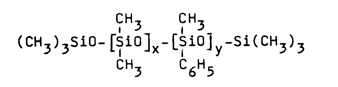
mit einem Methyl/Phenyl-Verhältnis von 20:1 und einer Viskosität von 2000 mPa.s (bei 25°C) wird mittels Spin-coating auf einen Siliciumwafer aufgebracht. Die Bestrahlung erfolgt in einer Reaktionskammer, durch die 15 min lang ein Stickstoffstrom geleitet wurde. Zur Bestrahlung dient ein mit einem Nd/YAG-Laser gepumpter Farbstofflaser, wobei folgende Bestrahlungsparameter eingehalten werden: unfokussierter Laserstrahl, Wellenlänge λ = 266 nm, Frequenz ν = 10 Hz, Impulsdauer t = 10 ns, Zahl der Impulse n = 1000, Energiedichte E ≈ 30 J/cm². Nach der Bestrahlung wird durch Behandeln mit Dichlormethan entwickelt, wobei die belichtete Stelle auf dem Siliciumwafer zurückbleibt; die Schichtdicke beträgt ca. 20 µm. - Ein Poly(dimethylsiloxan) folgender Struktur

mit einer Viskosität von 1000 mPa.s (bei 25°C) wird mittels Spin-coating auf einen Siliciumwafer aufgebracht. Die Bestrahlung erfolgt in einer Reaktionskammer, die 30 min lang bei einem Druck von 2 . 10⁻⁵ mbar evakuiert wurde. Zur Bestrahlung dient ein ArF-Laser, wobei folgende Bestrahlungsparameter eingehalten werden: unfokussierter Laserstrahl, λ = 193 nm, ν = 50 Hz, t = 30 ns, n = 1000, E ≈ 74 J/cm².
Nach der Bestrahlung wird durch Behandeln mit Dichlormethan entwickelt, wobei die belichtete Stelle auf dem Siliciumwafer zurückbleibt; die Schichtdicke beträgt ca. 2,5 µm. - Ein Poly(methylphenylsiloxan) entsprechend Beispiel 1, dem 0,5 Masse-% eines Methylvinylsiloxan/Dimethylsiloxan-Copolymeren mit einem Vinylgehalt von 7,5 % zugesetzt wurden, wird entsprechend Beispiel 1 auf einen Siliciumwafer aufgebracht und bestrahlt, wobei folgende Bestrahlungsparameter eingehalten werden: unfokussierter Laserstrahl, λ = 266 nm, ν = 10 Hz, t = 10 ns, n = 300, E ≈ 10 J/cm².
Nach der Bestrahlung wird durch Behandeln mit Dichlormethan entwickelt, wobei die belichtete Stelle auf dem Siliciumwafer zurückbleibt; die Schichtdicke beträgt ca. 20 µm.
Claims (10)
- Verfahren zur Erzeugung dünner Schichten auf Siliconbasis durch Photohärtung von Organosiloxanen, dadurch gekennzeichnet, daß nichtfunktionalisierte Organosiloxane mit Alkylgruppen oder Alkyl- und Arylgruppen photochemisch - ohne die Verwendung von Photoinitiatoren und/oder Photosensibilisatoren - mittels Impulslaserstrahlung mit einer Wellenlänge < 400 nm polymerisiert und/oder vernetzt werden, wobei die Impulsdauer 10 ps bis 1 ms, die Impulsfrequenz 1 Hz bis 10 kHz und die Energiedichte mindestens 1 J/cm² beträgt und die Bestrahlung mit einem oder mehreren Impulsen erfolgt.
- Verfahren nach Anspruch 1, dadurch gekennzeichnet, daß das Molverhältnis von Arylgruppen zu Alkylgruppen der Organosiloxane maximal 2,0 beträgt und vorzugsweise zwischen 0,001 und 0,5 liegt.
- Verfahren nach Anspruch 1 oder 2, dadurch gekennzeichnet, daß eine Impulslaserstrahlung mit einer Wellenlänge zwischen 190 und 300 nm verwendet wird.
- Verfahren nach einem der Ansprüche 1 bis 3, dadurch gekennzeichnet, daß ein Poly(dimethylsiloxan) eingesetzt wird und die Bestrahlung mit einer Wellenlänge von 193 nm erfolgt.
- Verfahren nach einem der Ansprüche 1 bis 3, dadurch gekennzeichnet, daß ein Poly(methylphenylsiloxan) eingesetzt wird und die Bestrahlung mit einer Wellenlänge von 240 bis 280 nm erfolgt.
- Verfahren nach einem oder mehreren der Ansprüche 1 bis 5, dadurch gekennzeichnet, daß den Organosiloxanen vinylgruppenhaltige Siloxane in einer Menge von 0,5 bis 1,0 Masse-% zugesetzt werden.
- Verfahren nach einem oder mehreren der Ansprüche 1 bis 6, dadurch gekennzeichnet, daß die Bestrahlung in sauerstofffreier Atmosphäre durchgeführt wird.
- Verfahren nach einem oder mehreren der Ansprüche 1 bis 7, dadurch gekennzeichnet, daß durch eine Maske bestrahlt wird.
- Verwendung der nach dem Verfahren nach einem oder mehreren der Ansprüche 1 bis 7 hergestellten dünnen Schichten als Passivier- und/oder Isolierschicht für diskrete Halbleiterbauelemente und integrierte Halbleiterschaltungen.
- Verwendung der nach dem Verfahren nach einem oder mehreren der Ansprüche 1 bis 8 hergestellten dünnen Schichten als strukturierte Passivier- und/oder Isolierschicht bei Halbleiterbauelementen.
Applications Claiming Priority (2)
| Application Number | Priority Date | Filing Date | Title |
|---|---|---|---|
| DE3826713 | 1988-08-05 | ||
| DE3826713 | 1988-08-05 |
Publications (3)
| Publication Number | Publication Date |
|---|---|
| EP0353583A2 EP0353583A2 (de) | 1990-02-07 |
| EP0353583A3 EP0353583A3 (en) | 1990-03-07 |
| EP0353583B1 true EP0353583B1 (de) | 1993-09-29 |
Family
ID=6360338
Family Applications (1)
| Application Number | Title | Priority Date | Filing Date |
|---|---|---|---|
| EP89113591A Expired - Lifetime EP0353583B1 (de) | 1988-08-05 | 1989-07-24 | Verfahren zur Erzeugung dünner Schichten auf Siliconbasis |
Country Status (3)
| Country | Link |
|---|---|
| US (1) | US4983419A (de) |
| EP (1) | EP0353583B1 (de) |
| DE (1) | DE58905751D1 (de) |
Families Citing this family (17)
| Publication number | Priority date | Publication date | Assignee | Title |
|---|---|---|---|---|
| GB9501287D0 (en) * | 1995-01-24 | 1995-03-15 | Ciba Geigy Ag | Surface treatment |
| RU2181134C2 (ru) * | 1996-07-23 | 2002-04-10 | Вантико Аг | Обработка поверхности металла |
| US6001297A (en) * | 1997-04-28 | 1999-12-14 | 3D Systems, Inc. | Method for controlling exposure of a solidfiable medium using a pulsed radiation source in building a three-dimensional object using stereolithography |
| JP3173426B2 (ja) * | 1997-06-09 | 2001-06-04 | 日本電気株式会社 | シリカ絶縁膜の製造方法及び半導体装置の製造方法 |
| DE19861329B4 (de) * | 1997-06-26 | 2006-02-02 | Mitsubishi Denki K.K. | Struktur eines Zwischenschichtisolierfilmes in einer Halbleitereinrichtung |
| RU2160748C2 (ru) * | 1998-02-16 | 2000-12-20 | Акционерное общество закрытого типа "Тетра" | Способ получения тонкопленочного материала |
| GB9810917D0 (en) * | 1998-05-21 | 1998-07-22 | Trikon Technologies Ltd | Method and apparatus for treating a semi-conductor substrate |
| US7923383B2 (en) * | 1998-05-21 | 2011-04-12 | Tokyo Electron Limited | Method and apparatus for treating a semi-conductor substrate |
| US6121130A (en) * | 1998-11-16 | 2000-09-19 | Chartered Semiconductor Manufacturing Ltd. | Laser curing of spin-on dielectric thin films |
| EP1106653A3 (de) * | 1999-11-19 | 2002-03-20 | Dow Corning Asia, Ltd. | Verfahren zur Photohärtung von Polyorganosiloxane und Polyorganosiloxanzusammensetzung für optische Zwecke |
| US20050032357A1 (en) * | 2002-01-17 | 2005-02-10 | Rantala Juha T. | Dielectric materials and methods for integrated circuit applications |
| US20040002617A1 (en) * | 2002-01-17 | 2004-01-01 | Rantala Juha T. | Integrated circuits having organic-inorganic dielectric materials and methods for forming such integrated circuits |
| US7060634B2 (en) * | 2002-01-17 | 2006-06-13 | Silecs Oy | Materials and methods for forming hybrid organic-inorganic dielectric materials for integrated circuit applications |
| US7938783B2 (en) * | 2003-08-19 | 2011-05-10 | Advanced Monitors Corporation | Medical body core thermometer |
| DE102004020328A1 (de) * | 2004-04-26 | 2005-11-03 | Infineon Technologies Ag | Verfahren zur Abscheidung einer mit Kohlenstoff dotierten siliziumhaltigen dielektrischen Schicht |
| EP1615260A3 (de) | 2004-07-09 | 2009-09-16 | JSR Corporation | Auf organischem Siliziumoxid basierende Schicht, Zusammensetzung, und Verfahren zur Herstellung davon, und Halbleiteranordnung |
| US20150253901A1 (en) * | 2014-03-07 | 2015-09-10 | Cn Innovations Limited | Manufacturing method for single-sided multi-layer circuit pattern for touch panel |
Family Cites Families (5)
| Publication number | Priority date | Publication date | Assignee | Title |
|---|---|---|---|---|
| US3915824A (en) * | 1973-03-30 | 1975-10-28 | Scm Corp | Uv and laser curing of the polymerizable binder |
| JPS57181326A (en) * | 1981-04-28 | 1982-11-08 | Mitsubishi Heavy Ind Ltd | Laser hardening method |
| JPS59154029A (ja) * | 1983-02-23 | 1984-09-03 | Nippon Telegr & Teleph Corp <Ntt> | 絶縁膜形成方法 |
| US4526807A (en) * | 1984-04-27 | 1985-07-02 | General Electric Company | Method for deposition of elemental metals and metalloids on substrates |
| EP0202803A3 (de) * | 1985-05-14 | 1987-06-03 | Commonwealth Of Australia Department Of Industry Technology And Commerce | Aushärten mit Laser von Beschichtungen und Tinten |
-
1989
- 1989-07-21 US US07/384,291 patent/US4983419A/en not_active Expired - Fee Related
- 1989-07-24 EP EP89113591A patent/EP0353583B1/de not_active Expired - Lifetime
- 1989-07-24 DE DE89113591T patent/DE58905751D1/de not_active Expired - Fee Related
Also Published As
| Publication number | Publication date |
|---|---|
| US4983419A (en) | 1991-01-08 |
| EP0353583A2 (de) | 1990-02-07 |
| EP0353583A3 (en) | 1990-03-07 |
| DE58905751D1 (de) | 1993-11-04 |
Similar Documents
| Publication | Publication Date | Title |
|---|---|---|
| EP0353583A2 (de) | Verfahren zur Erzeugung dünner Schichten auf Siliconbasis | |
| DE69213482T2 (de) | Beschichtungszusammensetzung zum Herstellen von isolierenden Schichten und Masken | |
| DE69637166T2 (de) | Verfahren zur Härtung eines Wasserstoff-Silsesquioxanharzes mittels Elektronenstrahlen zur Umwandlung in eine Silika enthaltende Keramikbeschichtung | |
| DE69913457T2 (de) | Überzüge auf Vinyletherbasis für optische Fasern | |
| DE69127009T2 (de) | UV-härtbare, vorvernetzte, epoxyfunktionelle Silicone | |
| EP0336141B1 (de) | Verfahren zum Beschichten von flächigen Trägern durch Aufbringen von mit (Meth)acrylsäureestergruppen modifizierten härtbaren Organopolysiloxanen | |
| EP0101587B1 (de) | Positiv arbeitendes Verfahren zur Herstellung von Reliefbildern oder Resistmustern | |
| EP0506616B1 (de) | Photoempfindliches Gemisch auf Basis von Acrylaten | |
| DE3546801C2 (de) | ||
| EP0604364B1 (de) | Neue (cyclo)aliphatische Epoxidverbindungen | |
| DE19800633B4 (de) | Verfahren und Vorrichtung unter Verwendung eines ArF Photoresists | |
| DE19615489A1 (de) | UV-härtbare Epoxysilicon-Mischungszusammensetzungen | |
| DE2804283A1 (de) | Wasserfreie polymerisierbare massen auf basis von hydrolysierbaren silanen und verfahren zur kondensation von hydrolysierbaren silanen | |
| HK1005623B (en) | New(cyclo) aliphatic epoxy compounds | |
| DE2520775A1 (de) | Lichtempfindliche harzzusammensetzung | |
| DE3006167A1 (de) | Fotovernetzbare organopolysiloxan- materialien | |
| DE2207853A1 (de) | Photoempfindliche, dielektrische Zusammensetzung | |
| US4939065A (en) | UV-curable organopolysiloxane compositions and negative photoresists comprised thereof | |
| WO2009021256A1 (de) | Verfahren zur herstellung von optischen polymer-wellenleitern basierend auf einem organopolysiloxan sowie leiterplatte und verwendung | |
| DE69725041T2 (de) | UV härtbare Masse und Verfahren zur Bildung von Mustern aus gehärteten Produkten derselben | |
| JPH04306222A (ja) | Uv硬化性エポキシシリコ―ン | |
| JP5563589B2 (ja) | 非線形熱重合を使用した三次元物品 | |
| DE69311726T2 (de) | Schnell härtbare vinylethertrennbeschichtungen | |
| DE60007348T2 (de) | Verwendung von beschleunigern für die polymerisation und/oder vernetzung von polyorganosiloxanen mit vernetzbaren funktionellen gruppen, entsprechende zusammensetzungen | |
| DE4126759A1 (de) | Verfahren zur erzeugung siliciumhaltiger organischer schichten |
Legal Events
| Date | Code | Title | Description |
|---|---|---|---|
| PUAI | Public reference made under article 153(3) epc to a published international application that has entered the european phase |
Free format text: ORIGINAL CODE: 0009012 |
|
| PUAL | Search report despatched |
Free format text: ORIGINAL CODE: 0009013 |
|
| AK | Designated contracting states |
Kind code of ref document: A2 Designated state(s): DE FR GB IT NL |
|
| AK | Designated contracting states |
Kind code of ref document: A3 Designated state(s): DE FR GB IT NL |
|
| 17P | Request for examination filed |
Effective date: 19900905 |
|
| 17Q | First examination report despatched |
Effective date: 19920122 |
|
| GRAA | (expected) grant |
Free format text: ORIGINAL CODE: 0009210 |
|
| AK | Designated contracting states |
Kind code of ref document: B1 Designated state(s): DE FR GB IT NL |
|
| REF | Corresponds to: |
Ref document number: 58905751 Country of ref document: DE Date of ref document: 19931104 |
|
| ET | Fr: translation filed | ||
| ITF | It: translation for a ep patent filed | ||
| GBT | Gb: translation of ep patent filed (gb section 77(6)(a)/1977) |
Effective date: 19931223 |
|
| PGFP | Annual fee paid to national office [announced via postgrant information from national office to epo] |
Ref country code: GB Payment date: 19940616 Year of fee payment: 6 |
|
| PGFP | Annual fee paid to national office [announced via postgrant information from national office to epo] |
Ref country code: FR Payment date: 19940725 Year of fee payment: 6 |
|
| PLBE | No opposition filed within time limit |
Free format text: ORIGINAL CODE: 0009261 |
|
| STAA | Information on the status of an ep patent application or granted ep patent |
Free format text: STATUS: NO OPPOSITION FILED WITHIN TIME LIMIT |
|
| PGFP | Annual fee paid to national office [announced via postgrant information from national office to epo] |
Ref country code: NL Payment date: 19940731 Year of fee payment: 6 |
|
| PGFP | Annual fee paid to national office [announced via postgrant information from national office to epo] |
Ref country code: DE Payment date: 19940915 Year of fee payment: 6 |
|
| 26N | No opposition filed | ||
| PG25 | Lapsed in a contracting state [announced via postgrant information from national office to epo] |
Ref country code: GB Effective date: 19950724 |
|
| PG25 | Lapsed in a contracting state [announced via postgrant information from national office to epo] |
Ref country code: NL Effective date: 19960201 |
|
| GBPC | Gb: european patent ceased through non-payment of renewal fee |
Effective date: 19950724 |
|
| NLV4 | Nl: lapsed or anulled due to non-payment of the annual fee |
Effective date: 19960201 |
|
| PG25 | Lapsed in a contracting state [announced via postgrant information from national office to epo] |
Ref country code: DE Effective date: 19960402 |
|
| PG25 | Lapsed in a contracting state [announced via postgrant information from national office to epo] |
Ref country code: FR Effective date: 19960430 |
|
| REG | Reference to a national code |
Ref country code: FR Ref legal event code: ST |
|
| REG | Reference to a national code |
Ref country code: FR Ref legal event code: ST |
|
| REG | Reference to a national code |
Ref country code: FR Ref legal event code: ST |
|
| PG25 | Lapsed in a contracting state [announced via postgrant information from national office to epo] |
Ref country code: IT Free format text: LAPSE BECAUSE OF NON-PAYMENT OF DUE FEES;WARNING: LAPSES OF ITALIAN PATENTS WITH EFFECTIVE DATE BEFORE 2007 MAY HAVE OCCURRED AT ANY TIME BEFORE 2007. THE CORRECT EFFECTIVE DATE MAY BE DIFFERENT FROM THE ONE RECORDED. Effective date: 20050724 |