EP0333583B1 - Verfahren zur Herstellung einer Halbleitervorrichtung - Google Patents
Verfahren zur Herstellung einer Halbleitervorrichtung Download PDFInfo
- Publication number
- EP0333583B1 EP0333583B1 EP89400710A EP89400710A EP0333583B1 EP 0333583 B1 EP0333583 B1 EP 0333583B1 EP 89400710 A EP89400710 A EP 89400710A EP 89400710 A EP89400710 A EP 89400710A EP 0333583 B1 EP0333583 B1 EP 0333583B1
- Authority
- EP
- European Patent Office
- Prior art keywords
- type impurity
- impurity ions
- conductivity type
- implanting
- ions
- Prior art date
- Legal status (The legal status is an assumption and is not a legal conclusion. Google has not performed a legal analysis and makes no representation as to the accuracy of the status listed.)
- Expired - Lifetime
Links
Images


Classifications
-
- H—ELECTRICITY
- H10—SEMICONDUCTOR DEVICES; ELECTRIC SOLID-STATE DEVICES NOT OTHERWISE PROVIDED FOR
- H10B—ELECTRONIC MEMORY DEVICES
- H10B20/00—Read-only memory [ROM] devices
- H10B20/27—ROM only
- H10B20/30—ROM only having the source region and the drain region on the same level, e.g. lateral transistors
- H10B20/38—Doping programmed, e.g. mask ROM
- H10B20/383—Channel doping programmed
-
- H—ELECTRICITY
- H01—ELECTRIC ELEMENTS
- H01L—SEMICONDUCTOR DEVICES NOT COVERED BY CLASS H10
- H01L21/00—Processes or apparatus adapted for the manufacture or treatment of semiconductor or solid state devices or of parts thereof
- H01L21/02—Manufacture or treatment of semiconductor devices or of parts thereof
- H01L21/04—Manufacture or treatment of semiconductor devices or of parts thereof the devices having at least one potential-jump barrier or surface barrier, e.g. PN junction, depletion layer or carrier concentration layer
- H01L21/18—Manufacture or treatment of semiconductor devices or of parts thereof the devices having at least one potential-jump barrier or surface barrier, e.g. PN junction, depletion layer or carrier concentration layer the devices having semiconductor bodies comprising elements of Group IV of the Periodic System or AIIIBV compounds with or without impurities, e.g. doping materials
- H01L21/26—Bombardment with radiation
- H01L21/263—Bombardment with radiation with high-energy radiation
- H01L21/265—Bombardment with radiation with high-energy radiation producing ion implantation
Definitions
- the present invention relates to a method of producing a semiconductor device, and more particularly, to an ion implantation method of writing information in a Read Only Memory (ROM), etc.
- ROM Read Only Memory
- each cell is composed of the MOS transistor or a resistance.
- Vth the threshold voltage
- the control of the threshold voltage (Vth) is usually carried out before the gate electrode formation during the MOS transistor production process, due to the limitations (usually 200 KeV or less) of the accelerating energy of the ion implanting apparatus used to introduce impurities into a semiconductor.
- an ion implanting apparatus having a high accelerating energy of, e.g., 0.4 to 3 MeV, has been actually used and control of the Vth realized thereby, through a gate electrode and/or an insulating film positioned thereon.
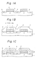
- Figures 1A to 1C are cross-sectional process views of a conventional method of implanting ions in a ROM.
- a p type silicon substrate 1 is provided with n+ source/drain regions 2 and 3 on which is formed a gate electrode 4 having a 20 nm (200 ⁇ ) thick gate silicon oxide film 5.
- ROM information is written by implanting n type impurity ions, for example Phosphorus (P+), in the silicon substrate 1 through the gate electrode 4 and the gate silicon oxide film 5 with an energy of about 100 to 200 KeV, so that an n-type region having a depth of about 0.2 ⁇ m or less is formed.
- n type impurity ions for example Phosphorus (P+)
- a wiring or interconnection forming process and a passivation process are carried out as shown in Fig. 1C, and a final ROM product, is produced.
- Fig. 1C 8 denotes a passivation film, etc. In this process, however, the turnaround time from information writing to final product is a lengthy period of one week or more.
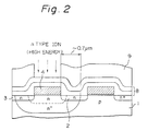
- Figure 2 shows a cross-sectional view of another conventional example, wherein impurity ions having a high energy are implanted, from above insulating films (passivation film 5, etc.) 8 formed on a gate electrode 4, in a p-type silicon substrate 1.
- n-type impurities e.g., P+, having a high energy of 0.4 to 3 MeV are implanted from above the passivation films etc. 8 formed on a gate electrode 4, in a p type silicon substrate 1.
- This high energy implanting method shortens the turnaround time from the ion implanting process to the final product to, for example, two or three days.
- the implanting distance of ions is lengthened by using the high energy implanting apparatus the ion spread in the lateral direction is made wider (0.7 ⁇ m in Fig. 2) and the widened region has an adverse influence on an adjacent cell when information writing in a cell. This problem has become more serious with the need for a shrinkage of the cells in a ROM.
- the ion implanting energy is increased, the ion-spread in the lateral direction is greater, and thus, it is difficult to shrink ROM cells beyond a certain limit.
- a width of about 0.2 - 0.4 ⁇ m occurs to a region having a concentration one-tenth that of the implanting region.
- the present inventor proposed an ion implanting method disclosed in a Japanese Unexamined Patent Publication (Kokai) No. 63-299119 wherein, during a high energy ion implantation, opposite conductive type impurity ions (compensating ions) having a wider region in the lateral direction than that of the writing ions are implanted at a low dose from the opening of the same mask as used for the writing, so that the conductive type is compensated at a tail portion.
- An object of the present invention is to solve the above-mentioned problems.
- a further object of the present invention is to provide a method of producing a semiconductor device such as a ROM, wherein information can be written in a ROM by an ion implanting process using optional ions, in accordance with a design of a cell structure.
- a still further object of the present invention is to provide a method of producing a semiconductor device such as ROM, wherein a greater shrinkage of cells can be realized.
- An additional object of the present invention is to provide a method of producing a semiconductor device such as a ROM wherein a turnaround time from a ion implantation to produce completion is shortened.
- a method of producing a semiconductor device comprising the steps of: forming a gate insulating layer on a semiconductor substrate, forming a gate electrode on the gate insulating layer, forming a source/drain region in the semiconductor substrate, forming a cover layer on the entire exposed surface, forming a mask on the cover layer having an opening over the gate electrode, implanting a first conductivity type impurity ions into the semiconductor substrate through the cover layer, the gate electrode and the gate insulating layer as the first ion implanting process, implanting in a second implanting process a second conductivity type impurity ions, opposite to the first conductivity type, into the semiconductor substrate at an implanting angle larger than that used in the first ion implanting process with respect to the normal plane of the semiconductor substrate and to substantially the same depth as the first ion implanting process and at a dosage smaller than in the first ion implanting process, whereby said one conductivity type impurity ions are compensated at laterally spread portions
- the order of the first ion implanting process and the second ion implanting process can be swapped, of course.
- the compensating ion distribution in the substrate can sometimes reach the adjacent cell, the direction of shift of the threshold voltage is opposite to that for the writing ions, and thus the device functions without problem.
- the first conductivity type impurity ions are preferably implanted at an implanting angle of 0 to 7°, particularly 0° with respect to the normal plane of the semiconductor device, at a projective range of 0.5 to 3 ⁇ m, particularly about 1,7 ⁇ m, and a dosage of 1 to 5 x 10¹³/cm2, particularly about 1.2 x 10¹³/cm2.
- the second conductivity type impurity ions are preferably implanted at an implanting angle of larger than 7°; particularly about 10°, at a projective range of 0.5 to 3 ⁇ m particularly about 1,7 ⁇ m, and a dosage of 1 to 5 x 10¹²/cm2, particularly, about 2.5 x 10¹²/cm2.
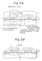
- Figures 3A and 3B are cross-sectional process views of a ROM cell for explaining an example according to the present invention.
- a gate electrode 4 provided with a 20 nm (200 ⁇ ) thick gate SiO2 film 5 is formed by a usual process on a p type silicon substrate 1 having n+ source/drain regions 2 and 3 of a cell transistor.
- the gate electrode 4 is made of polycrystalline silicon (poly Si) having a thickness of 400 nm (4000 ⁇ ), and a phospho-silicate glass (PSG) interlayer insulating film 10 having a thickness of 500 nm (5000 ⁇ ) and a PSG cover film 11 having a thickness of 600 nm (6000 ⁇ ) are formed on the gate electrode 4.
- the gate length L of the cell transistor is 0.8 ⁇ m and the cell gap D is 0.8 ⁇ m.
- a mask 12 comprising tungsten 300 nm (3000 ⁇ ) and resist 500 nm (5000 ⁇ ), for ion implantation for writing information, is formed on the PSG cover film 11.
- a slight deviation ( ⁇ L) between the mask opening and the cell pattern can be for seen (not shown).
- the information is written by controlling a threshold voltage of the cell transistor, as mentioned before.
- the threshold voltage control is effected by implanting writing ions into a channel forming region of the Si substrate 1 through covered insulating films and the poly Si gate having a total thickness of 1.5 ⁇ m.
- Phosphorus ions (P+) having a n conductivity type are used as the writing ions.
- the P+ ion implanting conditions are as follows: implanting energy, 1.5 MeV, dosage: 1.2 x 10¹³/cm2, and implanting angle ⁇ : 0°.
- B+ boron ions having an p conductivity type
- the B+ ion implanting conditions are as follows; implanting energy: 0.75 MeV, dosage: 2.5 x 10¹²/cm ⁇ 2, and implanting angle ⁇ : 10°.
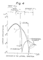
- Figure 4 is a graph illustrating an impurity distribution or profile of the above conventional examples.
- the ordinate axis is a carrier concentration which is equal to the absolute value of the difference between the n type impurity concentration and the p type impurity concentration at an ordinary temperature
- the transverse axis is a distance in a lateral direction.
- the ions are annealed at a usual temperature of 600°C or less (in this case, 600°C), for 30 minutes.
- the spread in the lateral direction of the implanted ion is about 0.7 ⁇ m, as also shown in Fig. 3A and 4.
- the distance 0.7 ⁇ m possibly covers a part of the adjacent cell and shifts the threshold voltage to a depression side. This occurs when the mask is deviated and the gap between the cell and the adjacent cell is narrowed.
- the carrier concentration in a writing cell is little varied and the distance of the n type region is reduced to 0.2 ⁇ m by the distribution (broken line X) of Boron (B+) having the opposite conductivity type to that of P+, so that the n type region does not reach the adjacent cell.
- n type region is reversed to a p type region by implanting p type ions with a tilted angle, and thus as shown in Fig. 3B, an n type region having a lesser spread is formed as information written in a ROM cell.
- Figures 5A to 5C are cross-sectional views taken along the line AA of Figure 7, for explaining another example of the present invention.
- Figure 5A shows a P+ ion (writing ion) implanted state.
- Figure 5B shows a B+ ion (compensating ion) implanted state
- Figure 5C shows a (P+) - (B+), i.e., compensated, state.
- Figs. 5A to 5C except that the resist mask 12 and the tungsten mask 13 are slightly deviated (e.g., 0.3 ⁇ m) to the right side, the various conditions (e.g., ion implantation and thickness) are substantially the same as shown in the example of Figs. 3A and 3B.
- the P+ (n type) ion implanted width in the lateral direction from P to Q is about 0.85 ⁇ m
- the B+ (p type) ion implanted spread in the lateral direction from R to S is about 0.95 ⁇ m
- the compensated ion implanted spread in the lateral direction T to U is about 0.55 ⁇ m, and thus is reduced by 0.3 ⁇ m.
- Figures 6A to 6C are cross-sectional views taken along the line BB of Figure 7 for explaining another example of the present invention.
- Figure 6A shows a P+ ion (writing ion) implanted state
- Figure 6B shows a B+ ion (compensating ion) implanted state
- Figure 6C shows a (P+) - (B+), i.e., compensated, state.
- Figs. 6A to 6C except that the resist mask 12 and the tungsten mask 13 are slightly deviated (e.g., 0.3 ⁇ m) to the right side, the various conditions (e.g., ion implantation, and thickness) are substantially the same as in the example shown in Figs. 3A and 3B.
- a field oxide film (SiO2) 15 having a thickness of 600 nm (6000 ⁇ ) is provided, and as can be seen in Figs. 6A to 6C the compensated ion spread in the lateral direction is reduced by about 0.45 ⁇ m, and thus the spread thereof does not cover the adjacent cell.
Claims (12)
- Ein Verfahren zum Herstellen einer Halbleiteranordnung mit den Schritten:
Bilden einer Gateisolierschicht (5) auf einem Halbleitersubstrat (1),
Bilden einer Gateelektrode (4) auf der Gateisolierschicht,
Bilden einer Source-/Drainzone (2, 3) in dem Halbleitersubstrat,
Bilden einer Deckschicht (10, 11) auf der gesamten freiliegenden Oberfläche,
Bilden einer Maske (12) auf der Deckschicht, die über der Gateelektrode eine Öffnung hat,
Implantieren von Verunreinigungsionen eines ersten Leitfähigkeitstyps in das Halbleitersubstrat durch die Deckschicht, die Gateelektrode und die Gateisolierschicht als erstes Ionenimplantationsverfahren,
Implantieren von Verunreinigungsionen eines zweiten Leitfähigkeitstyps, der zum ersten Leitfähigkeitstyp entgegengesetzt ist, in das Halbleitersubstrat bei einem zweiten Implantationsverfahren, mit einem Implantationswinkel, der bezüglich der normalen Ebene des Halbleitersubstrats größer als jener des ersten Ionenimplantationsverfahrens ist, und im wesentlichen mit derselben Tiefe wie bei dem ersten Ionenimplantationsverfahren und mit einer kleineren Dosierung als bei dem ersten Ionenimplantationsverfahren, wodurch die Verunreinigungsionen des genannten einen Leitfähigkeitstyps an seitlich ausgebreiteten Abschnitten kompensiert werden. - Ein Verfahren nach Anspruch 1, bei dem das genannte Halbleitersubstrat (1) ein p-Typ-Siliziumsubstrat ist.
- Ein Verfahren nach Anspruch 1, bei dem die genannte Gateelektrode (4) eine polykristalline Siliziumelektrode mit einer Dicke von etwa 400 nm (4000 Å) ist.
- Ein Verfahren nach Anspruch 1, bei dem die genannte Deckschicht (10, 11), die auf der gesamten freiliegenden Oberfläche positioniert ist, aus zwei Phosphorsilikatglasschichten mit einer Gesamtdicke von 1,1 µm besteht.
- Ein Verfahren nach Anspruch 1, bei dem die Verunreinigungsionen des genannten ersten Leitfähigkeitstyps n-Typ-Verunreinigungsionen sind.
- Ein Verfahren nach Anspruch 5, bei dem die genannten n-Typ-Verunreinigungsionen Phosphorionen (P⁺) sind.
- Ein Verfahren nach Anspruch 1, bei dem die genannten Verunreinigungsionen des ersten Leitfähigkeitstyps mit einem Implantationswinkel von 0 bis 7° bezüglich der normalen Ebene der Halbleiteranordnung implantiert werden.
- Ein Verfahren nach Anspruch 1, bei dem die Verunreinigungsionen des genannten ersten Leitfähigkeitstyps bei einem projektiven Bereich von 0,5 bis 3 µm und einer Dosierung von 1 bis 5 x 10¹³/cm² implantiert werden.
- Ein Verfahren nach Anspruch 1, bei dem die Verunreinigungsionen des genannten zweiten Leitfähigkeitstyps p-Typ-Verunreinigungsionen sind.
- Ein Verfahren nach Anspruch 9, bei dem die genannten p-Typ-Verunreinigungsionen Borionen (B⁺) sind.
- Ein Verfahren nach Anspruch 1, bei dem die Verunreinigungsionen des genannten zweiten Leitfähigkeitstyps mit einem Implantationswinkel von größer als 7° bezüglich der normalen Ebene der Halbleiteranordnung implantiert werden.
- Ein Verfahren nach Anspruch 1, bei dem die Verunreinigungsionen des genannten zweiten Leitfähigkeitstyps bei einem projektiven Bereich von 0,5 bis 3 µm und einer Dosierung von 1 bis 5 x 10¹²/cm² implantiert werden.
Applications Claiming Priority (2)
| Application Number | Priority Date | Filing Date | Title |
|---|---|---|---|
| JP60127/88 | 1988-03-14 | ||
| JP63060127A JP2706460B2 (ja) | 1988-03-14 | 1988-03-14 | イオン注入方法 |
Publications (3)
| Publication Number | Publication Date |
|---|---|
| EP0333583A2 EP0333583A2 (de) | 1989-09-20 |
| EP0333583A3 EP0333583A3 (en) | 1990-01-17 |
| EP0333583B1 true EP0333583B1 (de) | 1993-07-14 |
Family
ID=13133157
Family Applications (1)
| Application Number | Title | Priority Date | Filing Date |
|---|---|---|---|
| EP89400710A Expired - Lifetime EP0333583B1 (de) | 1988-03-14 | 1989-03-14 | Verfahren zur Herstellung einer Halbleitervorrichtung |
Country Status (5)
| Country | Link |
|---|---|
| US (1) | US4889820A (de) |
| EP (1) | EP0333583B1 (de) |
| JP (1) | JP2706460B2 (de) |
| KR (1) | KR930000612B1 (de) |
| DE (1) | DE68907507T2 (de) |
Families Citing this family (26)
| Publication number | Priority date | Publication date | Assignee | Title |
|---|---|---|---|---|
| JPH0783122B2 (ja) * | 1988-12-01 | 1995-09-06 | 富士電機株式会社 | 半導体装置の製造方法 |
| US5270226A (en) * | 1989-04-03 | 1993-12-14 | Matsushita Electric Industrial Co., Ltd. | Manufacturing method for LDDFETS using oblique ion implantion technique |
| KR940010930B1 (ko) * | 1990-03-13 | 1994-11-19 | 가부시키가이샤 도시바 | 반도체장치의 제조방법 |
| JPH0487370A (ja) * | 1990-07-30 | 1992-03-19 | Sharp Corp | 半導体装置の製造方法 |
| US5155369A (en) * | 1990-09-28 | 1992-10-13 | Applied Materials, Inc. | Multiple angle implants for shallow implant |
| US5268317A (en) * | 1991-11-12 | 1993-12-07 | Siemens Aktiengesellschaft | Method of forming shallow junctions in field effect transistors |
| US5648288A (en) * | 1992-03-20 | 1997-07-15 | Siliconix Incorporated | Threshold adjustment in field effect semiconductor devices |
| JP3202784B2 (ja) * | 1992-04-13 | 2001-08-27 | 三菱電機株式会社 | マスクrom半導体装置およびその製造方法 |
| JPH06169089A (ja) * | 1992-05-07 | 1994-06-14 | Nec Corp | 縦型mosfetの製造方法 |
| JP3181695B2 (ja) * | 1992-07-08 | 2001-07-03 | ローム株式会社 | Soi基板を用いた半導体装置の製造方法 |
| US5559044A (en) * | 1992-09-21 | 1996-09-24 | Siliconix Incorporated | BiCDMOS process technology |
| US5736420A (en) * | 1993-08-20 | 1998-04-07 | National Semiconductor Corporation | Process for fabricating read only memories, with programming step performed midway through the fabrication process |
| EP0696054B1 (de) | 1994-07-04 | 2002-02-20 | STMicroelectronics S.r.l. | Verfahren zur Herstellung von Leistungsbauteilen hoher Dichte in MOS-Technologie |
| FR2730345B1 (fr) * | 1995-02-03 | 1997-04-04 | Matra Mhs | Procede de fabrication d'une memoire morte en technologie mos, et memoire ainsi obtenue |
| KR0147627B1 (ko) * | 1995-04-11 | 1998-11-02 | 김광호 | 낸드형 불휘발성 기억장치 |
| JP3419606B2 (ja) * | 1995-09-14 | 2003-06-23 | 富士通株式会社 | 半導体装置とその製造方法 |
| US5851886A (en) * | 1995-10-23 | 1998-12-22 | Advanced Micro Devices, Inc. | Method of large angle tilt implant of channel region |
| US6027978A (en) * | 1997-01-28 | 2000-02-22 | Advanced Micro Devices, Inc. | Method of making an IGFET with a non-uniform lateral doping profile in the channel region |
| JP3185862B2 (ja) | 1997-09-10 | 2001-07-11 | 日本電気株式会社 | マスク型半導体装置の製造方法 |
| DE19815873A1 (de) * | 1998-04-08 | 1999-10-14 | Siemens Ag | Verfahren zur Herstellung einer Halbleiter-Speichervorrichtung |
| US6074920A (en) * | 1998-08-26 | 2000-06-13 | Texas Instruments Incorporated | Self-aligned implant under transistor gate |
| US6632728B2 (en) | 2001-07-16 | 2003-10-14 | Agere Systems Inc. | Increasing the electrical activation of ion-implanted dopants |
| US6764909B2 (en) * | 2002-01-14 | 2004-07-20 | Texas Instruments Incorporated | Structure and method of MOS transistor having increased substrate resistance |
| US20120137971A1 (en) * | 2010-12-03 | 2012-06-07 | Vanrian Semiconductor Equipment Associates, Inc. | Hydrophobic property alteration using ion implantation |
| CN112735949B (zh) * | 2019-10-29 | 2023-06-06 | 中芯国际集成电路制造(上海)有限公司 | 半导体结构及其形成方法 |
| CN112018038B (zh) * | 2020-10-27 | 2021-02-19 | 晶芯成(北京)科技有限公司 | 一种半导体器件的制备方法 |
Family Cites Families (11)
| Publication number | Priority date | Publication date | Assignee | Title |
|---|---|---|---|---|
| US3615875A (en) * | 1968-09-30 | 1971-10-26 | Hitachi Ltd | Method for fabricating semiconductor devices by ion implantation |
| DE2802838A1 (de) * | 1978-01-23 | 1979-08-16 | Siemens Ag | Mis-feldeffekttransistor mit kurzer kanallaenge |
| JPS5939906B2 (ja) * | 1978-05-04 | 1984-09-27 | 超エル・エス・アイ技術研究組合 | 半導体装置の製造方法 |
| GB2056168A (en) * | 1979-08-01 | 1981-03-11 | Gen Instrument Corp | Method of fabricating P-N junction with high breakdown voltage |
| JPS56126970A (en) * | 1980-03-11 | 1981-10-05 | Nippon Telegr & Teleph Corp <Ntt> | Mos field effect transistor and manufacture thereof |
| US4417385A (en) * | 1982-08-09 | 1983-11-29 | General Electric Company | Processes for manufacturing insulated-gate semiconductor devices with integral shorts |
| JPS59100574A (ja) * | 1982-11-30 | 1984-06-09 | Sumitomo Electric Ind Ltd | シヨツトキゲ−ト電界効果トランジスタとその製造方法 |
| JPS61214457A (ja) * | 1985-03-19 | 1986-09-24 | Toshiba Corp | 半導体装置およびその製造方法 |
| JPS61292358A (ja) * | 1985-06-19 | 1986-12-23 | Fujitsu Ltd | Mis型電界効果トランジスタの製造方法 |
| JPS63278328A (ja) * | 1987-05-11 | 1988-11-16 | Matsushita Electronics Corp | 半導体容量素子の製造方法 |
| JPH0821555B2 (ja) * | 1987-05-28 | 1996-03-04 | 富士通株式会社 | イオン注入方法 |
-
1988
- 1988-03-14 JP JP63060127A patent/JP2706460B2/ja not_active Expired - Fee Related
-
1989
- 1989-03-09 US US07/321,201 patent/US4889820A/en not_active Expired - Lifetime
- 1989-03-14 KR KR1019890003135A patent/KR930000612B1/ko not_active IP Right Cessation
- 1989-03-14 DE DE89400710T patent/DE68907507T2/de not_active Expired - Lifetime
- 1989-03-14 EP EP89400710A patent/EP0333583B1/de not_active Expired - Lifetime
Also Published As
| Publication number | Publication date |
|---|---|
| JP2706460B2 (ja) | 1998-01-28 |
| EP0333583A2 (de) | 1989-09-20 |
| KR890015368A (ko) | 1989-10-30 |
| DE68907507D1 (de) | 1993-08-19 |
| EP0333583A3 (en) | 1990-01-17 |
| DE68907507T2 (de) | 1993-10-21 |
| KR930000612B1 (ko) | 1993-01-25 |
| JPH01233759A (ja) | 1989-09-19 |
| US4889820A (en) | 1989-12-26 |
Similar Documents
| Publication | Publication Date | Title |
|---|---|---|
| EP0333583B1 (de) | Verfahren zur Herstellung einer Halbleitervorrichtung | |
| US5378641A (en) | Electrically conductive substrate interconnect continuity region and method of forming same with an angled implant | |
| US6482698B2 (en) | Method of manufacturing an electrically programmable, non-volatile memory and high-performance logic circuitry in the same semiconductor chip | |
| EP0171864B1 (de) | Verfahren zum Herstellen eines Feldeffekttransistors mit isoliertem Gate | |
| US5283455A (en) | Thin film field effect element having an LDD structure | |
| US4835740A (en) | Floating gate type semiconductor memory device | |
| US5348897A (en) | Transistor fabrication methods using overlapping masks | |
| EP0503205B1 (de) | EPROM und Verfahren zur Herstellung | |
| JPS5842276A (ja) | Mos電界効果トランジスタ集積回路の製造方法 | |
| US20030127681A1 (en) | Nonvolatile semiconductor memory device | |
| US5547884A (en) | Method of manufacturing a semiconductor memory device having a common source region | |
| US5194929A (en) | Nonvolatile semiconductor memory and a memory of manufacturing the same | |
| US5536957A (en) | MOS field effect transistor having source/drain regions surrounded by impurity wells | |
| US5536962A (en) | Semiconductor device having a buried channel transistor | |
| US5616948A (en) | Semiconductor device having electrically coupled transistors with a differential current gain | |
| US6417548B1 (en) | Variable work function transistor high density mask ROM | |
| US5545580A (en) | Multi-state read-only memory using multiple polysilicon selective depositions | |
| US5536669A (en) | Method for fabricating read-only-memory devices with self-aligned code implants | |
| GB2080024A (en) | Semiconductor Device and Method for Fabricating the Same | |
| US5976960A (en) | Method of forming an electrically conductive substrate interconnect continuity region with an angled implant | |
| US5242850A (en) | Method of manufacturing a semiconductor memory device having reduced parasitically doped layers | |
| EP0452817B1 (de) | Halbleiterbauelement mit MOS-Transistoren und Verfahren zu dessen Herstellung | |
| US5273914A (en) | Method of fabricating a CMOS semiconductor devices | |
| US5432109A (en) | Device method for manufacturing a semiconductor memory | |
| EP0227965B1 (de) | Verfahren zum Programmieren durch Ionen-Implantation von Nurlesespeichern-NMOS und ein dadurch erhaltener Nurlesespeicher-NMOS |
Legal Events
| Date | Code | Title | Description |
|---|---|---|---|
| PUAI | Public reference made under article 153(3) epc to a published international application that has entered the european phase |
Free format text: ORIGINAL CODE: 0009012 |
|
| AK | Designated contracting states |
Kind code of ref document: A2 Designated state(s): DE FR GB |
|
| PUAL | Search report despatched |
Free format text: ORIGINAL CODE: 0009013 |
|
| AK | Designated contracting states |
Kind code of ref document: A3 Designated state(s): DE FR GB |
|
| 17P | Request for examination filed |
Effective date: 19900702 |
|
| 17Q | First examination report despatched |
Effective date: 19920715 |
|
| GRAA | (expected) grant |
Free format text: ORIGINAL CODE: 0009210 |
|
| AK | Designated contracting states |
Kind code of ref document: B1 Designated state(s): DE FR GB |
|
| REF | Corresponds to: |
Ref document number: 68907507 Country of ref document: DE Date of ref document: 19930819 |
|
| ET | Fr: translation filed | ||
| PLBE | No opposition filed within time limit |
Free format text: ORIGINAL CODE: 0009261 |
|
| STAA | Information on the status of an ep patent application or granted ep patent |
Free format text: STATUS: NO OPPOSITION FILED WITHIN TIME LIMIT |
|
| 26N | No opposition filed | ||
| REG | Reference to a national code |
Ref country code: GB Ref legal event code: IF02 |
|
| PGFP | Annual fee paid to national office [announced via postgrant information from national office to epo] |
Ref country code: FR Payment date: 20050308 Year of fee payment: 17 |
|
| PGFP | Annual fee paid to national office [announced via postgrant information from national office to epo] |
Ref country code: GB Payment date: 20050309 Year of fee payment: 17 |
|
| PGFP | Annual fee paid to national office [announced via postgrant information from national office to epo] |
Ref country code: DE Payment date: 20050310 Year of fee payment: 17 |
|
| PG25 | Lapsed in a contracting state [announced via postgrant information from national office to epo] |
Ref country code: GB Free format text: LAPSE BECAUSE OF NON-PAYMENT OF DUE FEES Effective date: 20060314 |
|
| PG25 | Lapsed in a contracting state [announced via postgrant information from national office to epo] |
Ref country code: DE Free format text: LAPSE BECAUSE OF NON-PAYMENT OF DUE FEES Effective date: 20061003 |
|
| GBPC | Gb: european patent ceased through non-payment of renewal fee |
Effective date: 20060314 |
|
| REG | Reference to a national code |
Ref country code: FR Ref legal event code: ST Effective date: 20061130 |
|
| PG25 | Lapsed in a contracting state [announced via postgrant information from national office to epo] |
Ref country code: FR Free format text: LAPSE BECAUSE OF NON-PAYMENT OF DUE FEES Effective date: 20060331 |