EP0227965B1 - Verfahren zum Programmieren durch Ionen-Implantation von Nurlesespeichern-NMOS und ein dadurch erhaltener Nurlesespeicher-NMOS - Google Patents
Verfahren zum Programmieren durch Ionen-Implantation von Nurlesespeichern-NMOS und ein dadurch erhaltener Nurlesespeicher-NMOS Download PDFInfo
- Publication number
- EP0227965B1 EP0227965B1 EP86116625A EP86116625A EP0227965B1 EP 0227965 B1 EP0227965 B1 EP 0227965B1 EP 86116625 A EP86116625 A EP 86116625A EP 86116625 A EP86116625 A EP 86116625A EP 0227965 B1 EP0227965 B1 EP 0227965B1
- Authority
- EP
- European Patent Office
- Prior art keywords
- regions
- drain
- gate
- source
- nmos
- Prior art date
- Legal status (The legal status is an assumption and is not a legal conclusion. Google has not performed a legal analysis and makes no representation as to the accuracy of the status listed.)
- Expired
Links
- 238000000034 method Methods 0.000 title claims description 37
- 230000015654 memory Effects 0.000 title claims description 21
- 239000007943 implant Substances 0.000 title claims description 17
- ZOXJGFHDIHLPTG-UHFFFAOYSA-N Boron Chemical compound [B] ZOXJGFHDIHLPTG-UHFFFAOYSA-N 0.000 claims description 17
- 229910052796 boron Inorganic materials 0.000 claims description 17
- 230000015556 catabolic process Effects 0.000 claims description 7
- 230000000873 masking effect Effects 0.000 claims description 7
- 239000004065 semiconductor Substances 0.000 claims description 4
- 239000000758 substrate Substances 0.000 claims description 3
- 125000006850 spacer group Chemical group 0.000 claims description 2
- 239000012535 impurity Substances 0.000 claims 6
- 239000002019 doping agent Substances 0.000 claims 4
- 230000015572 biosynthetic process Effects 0.000 claims 1
- 230000003247 decreasing effect Effects 0.000 claims 1
- 238000000151 deposition Methods 0.000 claims 1
- 238000009413 insulation Methods 0.000 claims 1
- 238000004519 manufacturing process Methods 0.000 description 11
- 229910052785 arsenic Inorganic materials 0.000 description 6
- RQNWIZPPADIBDY-UHFFFAOYSA-N arsenic atom Chemical compound [As] RQNWIZPPADIBDY-UHFFFAOYSA-N 0.000 description 6
- 238000005516 engineering process Methods 0.000 description 4
- 238000009792 diffusion process Methods 0.000 description 3
- 230000010354 integration Effects 0.000 description 3
- 230000007423 decrease Effects 0.000 description 2
- 239000011159 matrix material Substances 0.000 description 2
- 238000012856 packing Methods 0.000 description 2
- 229910021420 polycrystalline silicon Inorganic materials 0.000 description 2
- 229920005591 polysilicon Polymers 0.000 description 2
- OAICVXFJPJFONN-UHFFFAOYSA-N Phosphorus Chemical compound [P] OAICVXFJPJFONN-UHFFFAOYSA-N 0.000 description 1
- 238000005229 chemical vapour deposition Methods 0.000 description 1
- 238000005530 etching Methods 0.000 description 1
- 230000000670 limiting effect Effects 0.000 description 1
- 238000001465 metallisation Methods 0.000 description 1
- 238000012986 modification Methods 0.000 description 1
- 230000004048 modification Effects 0.000 description 1
- 238000002161 passivation Methods 0.000 description 1
- 229910052698 phosphorus Inorganic materials 0.000 description 1
- 239000011574 phosphorus Substances 0.000 description 1
Images
Classifications
-
- H—ELECTRICITY
- H10—SEMICONDUCTOR DEVICES; ELECTRIC SOLID-STATE DEVICES NOT OTHERWISE PROVIDED FOR
- H10B—ELECTRONIC MEMORY DEVICES
- H10B20/00—Read-only memory [ROM] devices
Definitions
- the present invention relates to a method for ion implant programing NMOS read-only memories and a NMOS memory obtained thereby.
- ROMs read-only memories
- Such ROMs are produced according to two techniques: either with NAND logic, so as to achieve greater packing, or with NOR logic in order to achieve greater access speed.
- the production methods for the two types of memory are substantially different.
- the method normally employed for programing read-only memories comprising a matrix of NOR gates including NMOS devices or transistors consists of the ion implanting of boron in the channel of the transistors through a suitable programing mask.
- the threshold voltage of some transistors of the matrix, selected by the programing mask, by virtue of the boron implanting is increased to a value higher than that of the supply voltage. Accordingly these transistors are 'off' during the reading of the memory.
- the ion implant phase can be carried out in an intermediate phase during the fabrication of the transistors, or the active-area mask can be used, and in this case programing is performed during the first phase of the transistor fabrication.
- the programing and implanting during an intermediate phase, since this method, though it requires an additional mask, allows faster delivery times of the finished memories since it is performed during the production process at a much more advanced stage.
- the known British document teaches forming a plurality of NMOS devices with source, drain and channel regions, with the channel regions extending partially between the drain and source regions. Furthermore, said known document teaches forming a heavier doped P-type region at the source-channel junction in advance to the source forming step.
- the aim of the invention is to provide a method for ion implant programing NMOS read-only memories such as to allow the use of the abovesaid programing technique even for very-large-scale-integration devices even for future generations, according to the current trends.
- a particular object of the present invention is to provide a method allowing reduction of the oxide layers thickness to values matching the scale of integration being used, yet assuring the reliable operation of the ROMs thus produced.
- Not least object of the present invention is to provide a said method, consisting of single per se already-known and used technological phases, which can be provided with machines and techniques which are common in the electronics industry, so as to have costs which are comparable with those of the known devices.
- the present invention also relates to a NMOS read-only memory, programed by ion implanting even in the case of very-large-scale integration, yet maintaining the necessary reliability and safety in operation.
- Said NMOS read-only memory comprising a plurality of NMOS devices, some predetermined ones of which have a high concentration of boron in the channel, is characterized in that it has said high concentration of boron in the channel only proximate to the source junction.
- the invention is based on the appreciation that the two requirements regarding the increase of the integration scale and the maintainment of both breakdown and threshold voltages, which hitherto were believed to be conflicting ones as to the thickness of the oxide layer, are related to two different phenomena, in turn depending upon the concentration of boron in two different regions of the channel, so that by doping said channel differentially it is possible to drop below the limits set by the current technology. Particularly by increasing the concentration of boron in the channel only proximate to the source junction it is possible to increase the threshold voltage (or keep it constant as the gate oxide thickness decreases) without reducing the breakdown voltage.
- NMOS read-only memories in an intermediate phase of the production process thereof. More in detail, both described processes make use of the greater diffusion coefficient of boron with respect to arsenic; however other systems for increasing the concentration of boron in the channel only proximate to the source junction are also within the scope of the inventive concept.
- a first example of the method according to the invention is as follows.
- the conventional NMOS process is performed initially, which process comprises active-zone masking, some implanting maskings, direct contact masking as well as polysilicon masking for defining the gate.
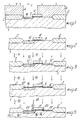
- an initial structure is obtained which is composed of a P type substrate 1, insulating oxides 2 and 3 and a polysilicon gate region 4.
- a programing masking step is performed, thereby a mask is obtained, which is open only at the source of the transistor to be programed.
- This mask is defined in Fig. 1 by the resist layer 6 having an opening at the substrate region which will form the source.
- a programing boron implant is performed (illustrated schematically in Fig. 1 by the arrows 7) so that a thin layer 10 with a high concentration of boron is formed.
- the resist layer 6 is removed and a process is performed at medium-high temperature such as to allow the diffusion of the boron in depth and laterally to achieve the P+ type channel region 10' such as to ensure the increase of the threshold voltage above the supply voltage, as is necessary for the correct operation of the device.
- a structure such as illustrated in Fig. 2 will thus be obtained.
- a heavy arsenic implant is performed at the source and at the drain of the device to be programed.
- This implant is schematically indicated by the arrows 11 in Fig. 3 and gives rise to the forming of the N type source region 12 and drain region 12'. Then the device is completed by standard NMOS phases, including masking for the contacts, metalization, and passivation.
- the method may be implemented as above explained up to the diffusion of the boron in the channel illustrated in Fig. 2, thereby obtaining the channel layer, indicated at 10'' of fig. 4.
- this implant is performed in two phases, respectively shown in Figs. 4 and 5. Accordingly, an initial light implant of phosphorus or arsenic is performed, as illustrated in Fig. 4 by the arrows 15, so as to form the source region 16 and the drain region 16' thin and lightly doped, followed by a spacer producing phase.
- This phase which is performed in a conventional manner by thermal oxide growth or by chemical vapour deposition and subsequent anisotropic etching without mask, allows to obtain the protection regions 20 at the vertical walls of the gate 4 (see Fig. 5).
- the invention fully achieves the intended aims. Indeed, a process and a memory are provided which, by virtue of the high concentration of boron at the source junction, has a threshold voltage with a suitable value, while the smaller concentration of boron in the channel at the drain junction keeps the breakdown voltage value high. Accordingly it is possible to reduce the thickness of the gate oxide layer to levels which are lower than those of the prior art, yet ensure the reliable operation of the so programed NMOS device of the read-only memory.
- the method described allows programing by implant, without using the active area mask, so that programing can be performed in a rather advanced fabrication step, with the advantages in delivery times already described above.
- process according to the invention makes use of phases which employ already-known technologies, for which machines which are common in the electronics industry are used, so as to keep the production costs comparable with those of similar devices.
Landscapes
- Semiconductor Memories (AREA)
Claims (3)
- Verfahren zum Programmieren durch Ionen-Implantation von NMOS-Nurlesespeichern mit mehreren NMOS-Schaltkreisen mit jeweils Drain- und Source-Abschnitten (12, 12', 19, 19') und einem Kanalabschnitt (10', 10''), der sich mindestens teilweise zwischen den Source- und Drain-Abschnitten erstreckt, wobei das Verfahren die Schritte aufweist, Isolierfeldoxydabschnitte (2) auf einem Halbleiterkörper (1) einer ersten Leitfähigkeitsart auszubilden, wobei die Feldoxydabschnitte (2) die aktiven Bereiche der NMOS-Schaltkreise begrenzen, eine dünne Gate-Oxydschicht (3) auf dem Halbleiterkörper (1) in den aktiven Bereichen zu bilden, Gate-Abschnitte (4) auf der Gate-Oxydschicht (3) zu bilden, wahlweise Dotierungsverunreinigungen im Substrat (1) zur Ausbildung von stärker dotierten Abschnitten (10) der ersten Leitfähigkeitsart einzubringen und die Drain- und Source-Abschnitte (12, 12', 19, 19') der entgegengesetzten Leitfähigkeitsart in den aktiven Bereichen quer zu den Gate-Abschnitten (4) diffundieren zu lassen,
dadurch gekennzeichnet, daß zur Programmierung der NMOS-Schaltkreise mit der dünnen Gate-Oxydschicht (3) nach Ausbildung der Gate-Abschnitte (4) ein Programmierungsmaskierungsschritt durchgeführt wird, um eine Programmierungsmaske (6) aufzubringen, die den Halbleiterkörper (1) bedeckt und Öffnungen besitzt, die wahlweise auf die aktiven Bereiche an den Source-Abschnitten (12, 19) und an den benachbart zu den Source-Abschnitten (12, 19) gelegenen Teilen der Gate-Abschnitte (4) von einigen ausgewählten, in einem AUS-Zustand zu programmierenden NMOS-Bauelementen gerichtet sind, anschließend den Schritt zur Einbringung der Dotierungsverunreinigungen durchzuführen, um die Kanalabschnitte (10', 10'') der ausgewählten NMOS-Bauelemente nur an deren benachbart zu den Source-Abschnitten (12, 19) gelegenen Abschnitten stärker zu dotieren, so daß die Schwellwertspannung erhöht werden kann oder die Gate-Oxyddicke ohne Reduzierung der Durchschlagspannung verringert werden kann. - Verfahren nach Anspruch 1,
dadurch gekennzeichnet, daß der Schritt zur Einbringung von Dotierungsverunreinigungen einen Borimplantierungsschritt umfaßt. - Verfahren nach den Ansprüchen 1 und 2,
gekennzeichnet durch die Schritte, nach dem Einbringen von Dotierungsverunreinigungen Verunreinigungen der ersten N-Art zu implantieren, wo die Drain- und Source-Abschnitte (19, 19') auszubilden sind, Oxydabstandselemente (20) seitlich zu den Gate-Abschnitten (4) auszubilden und Verunreinigungen der zweiten N-Art an den Drain- und Source-Abschnitten (19, 19') zu implantieren, um im Drain-Abschnitt leicht dotierte Bauelemente zu erhalten.
Applications Claiming Priority (2)
| Application Number | Priority Date | Filing Date | Title |
|---|---|---|---|
| IT23180/85A IT1186430B (it) | 1985-12-12 | 1985-12-12 | Rpocedimento per la realizzazione di memorie a sola lettura in tecnologia nmos programmate mediante impiantazione ionica e memoria a sola lettura ottenuta mediante tale procedimento |
| IT2318085 | 1985-12-12 |
Publications (3)
| Publication Number | Publication Date |
|---|---|
| EP0227965A2 EP0227965A2 (de) | 1987-07-08 |
| EP0227965A3 EP0227965A3 (en) | 1987-08-12 |
| EP0227965B1 true EP0227965B1 (de) | 1992-08-19 |
Family
ID=11204608
Family Applications (1)
| Application Number | Title | Priority Date | Filing Date |
|---|---|---|---|
| EP86116625A Expired EP0227965B1 (de) | 1985-12-12 | 1986-11-29 | Verfahren zum Programmieren durch Ionen-Implantation von Nurlesespeichern-NMOS und ein dadurch erhaltener Nurlesespeicher-NMOS |
Country Status (4)
| Country | Link |
|---|---|
| EP (1) | EP0227965B1 (de) |
| JP (1) | JPH07118509B2 (de) |
| DE (1) | DE3686481T2 (de) |
| IT (1) | IT1186430B (de) |
Families Citing this family (6)
| Publication number | Priority date | Publication date | Assignee | Title |
|---|---|---|---|---|
| FR2623650B1 (fr) * | 1987-11-20 | 1992-10-16 | Sgs Thomson Microelectronics | Composant electronique monolithique muni d'un decodeur commun pour sa memoire morte et sa memoire de traitement |
| FR2623651B1 (fr) * | 1987-11-20 | 1992-11-27 | Sgs Thomson Microelectronics | Plan memoire et procede et prototype de definition d'un circuit integre electronique comportant un tel plan memoire |
| FR2623653B1 (fr) * | 1987-11-24 | 1992-10-23 | Sgs Thomson Microelectronics | Procede de test de cellules de memoire electriquement programmable et circuit integre correspondant |
| IT1239707B (it) * | 1990-03-15 | 1993-11-15 | St Microelectrics Srl | Processo per la realizzazione di una cella di memoria rom a bassa capacita' di drain |
| JP3202784B2 (ja) * | 1992-04-13 | 2001-08-27 | 三菱電機株式会社 | マスクrom半導体装置およびその製造方法 |
| EP0575688B1 (de) * | 1992-06-26 | 1998-05-27 | STMicroelectronics S.r.l. | Programmierung von LDD-ROM-Zellen |
Family Cites Families (5)
| Publication number | Priority date | Publication date | Assignee | Title |
|---|---|---|---|---|
| US4045811A (en) * | 1975-08-04 | 1977-08-30 | Rca Corporation | Semiconductor integrated circuit device including an array of insulated gate field effect transistors |
| US4208780A (en) * | 1978-08-03 | 1980-06-24 | Rca Corporation | Last-stage programming of semiconductor integrated circuits including selective removal of passivation layer |
| JPS5570072A (en) * | 1978-11-21 | 1980-05-27 | Chiyou Lsi Gijutsu Kenkyu Kumiai | Semiconductor read only memory |
| JPS58148448A (ja) * | 1982-03-01 | 1983-09-03 | Nippon Denso Co Ltd | 半導体romの製造方法 |
| GB2157489A (en) * | 1984-03-23 | 1985-10-23 | Hitachi Ltd | A semiconductor integrated circuit memory device |
-
1985
- 1985-12-12 IT IT23180/85A patent/IT1186430B/it active
-
1986
- 1986-11-29 EP EP86116625A patent/EP0227965B1/de not_active Expired
- 1986-11-29 DE DE8686116625T patent/DE3686481T2/de not_active Expired - Fee Related
- 1986-12-10 JP JP61294620A patent/JPH07118509B2/ja not_active Expired - Fee Related
Also Published As
| Publication number | Publication date |
|---|---|
| IT8523180A0 (it) | 1985-12-12 |
| DE3686481T2 (de) | 1993-04-01 |
| EP0227965A3 (en) | 1987-08-12 |
| EP0227965A2 (de) | 1987-07-08 |
| JPS62140459A (ja) | 1987-06-24 |
| JPH07118509B2 (ja) | 1995-12-18 |
| DE3686481D1 (de) | 1992-09-24 |
| IT1186430B (it) | 1987-11-26 |
Similar Documents
| Publication | Publication Date | Title |
|---|---|---|
| US6482698B2 (en) | Method of manufacturing an electrically programmable, non-volatile memory and high-performance logic circuitry in the same semiconductor chip | |
| US6211014B1 (en) | Three-dimensional, deep-trench, high-density read-only memory (ROM) and its manufacturing method | |
| US4080718A (en) | Method of modifying electrical characteristics of MOS devices using ion implantation | |
| US4701776A (en) | MOS floating gate memory cell and process for fabricating same | |
| US4649629A (en) | Method of late programming a read only memory | |
| US5270240A (en) | Four poly EPROM process and structure comprising a conductive source line structure and self-aligned polycrystalline silicon digit lines | |
| EP0333583B1 (de) | Verfahren zur Herstellung einer Halbleitervorrichtung | |
| KR100304678B1 (ko) | 배선을형성한후에수소이온으로문턱전압을변경시키는것이가능한전계효과트랜지스터를구비한반도체장치제조방법 | |
| US6159795A (en) | Low voltage junction and high voltage junction optimization for flash memory | |
| US6657249B2 (en) | Nonvolatile semiconductor memory device with peripheral circuit part comprising at least one of two transistors having lower conductive layer same perpendicular structure as a floating gate | |
| JPH0669463A (ja) | Lddセルを有するnorタイプrom | |
| US5585297A (en) | Method of manufacture of multi-state mask ROM and multi-state mask ROM device produced thereby | |
| US20020182793A1 (en) | Transistors having selectively doped channel regions | |
| EP0160003B1 (de) | Mos-speicherzelle mit schwimmendem gate und verfahren zu ihrer verfertigung | |
| US7838947B2 (en) | Read-only memory device coded with selectively insulated gate electrodes | |
| US5545580A (en) | Multi-state read-only memory using multiple polysilicon selective depositions | |
| EP0227965B1 (de) | Verfahren zum Programmieren durch Ionen-Implantation von Nurlesespeichern-NMOS und ein dadurch erhaltener Nurlesespeicher-NMOS | |
| US5242850A (en) | Method of manufacturing a semiconductor memory device having reduced parasitically doped layers | |
| US6214229B1 (en) | Treatment system for removing phosphorus | |
| US5091329A (en) | Method for programming mos and cmos rom memories | |
| WO1998044552A9 (en) | Method of manufacturing a non-volatile memory combining an eprom with a standard cmos process | |
| EP0914679A2 (de) | Herstellungsverfahren eines festwertspeichers der den epromprozess mit dem standard-cmos-prozess kombiniert | |
| WO1981002493A1 (en) | Self-aligned buried contact and method of making | |
| US5942786A (en) | Variable work function transistor high density mask ROM | |
| KR0147592B1 (ko) | 마스크-롬의 제조방법 |
Legal Events
| Date | Code | Title | Description |
|---|---|---|---|
| PUAI | Public reference made under article 153(3) epc to a published international application that has entered the european phase |
Free format text: ORIGINAL CODE: 0009012 |
|
| PUAL | Search report despatched |
Free format text: ORIGINAL CODE: 0009013 |
|
| AK | Designated contracting states |
Kind code of ref document: A2 Designated state(s): DE FR GB NL |
|
| AK | Designated contracting states |
Kind code of ref document: A3 Designated state(s): DE FR GB NL |
|
| 17P | Request for examination filed |
Effective date: 19880205 |
|
| 17Q | First examination report despatched |
Effective date: 19910116 |
|
| RAP1 | Party data changed (applicant data changed or rights of an application transferred) |
Owner name: SGS-THOMSON MICROELECTRONICS S.R.L. |
|
| GRAA | (expected) grant |
Free format text: ORIGINAL CODE: 0009210 |
|
| AK | Designated contracting states |
Kind code of ref document: B1 Designated state(s): DE FR GB NL |
|
| REF | Corresponds to: |
Ref document number: 3686481 Country of ref document: DE Date of ref document: 19920924 |
|
| ET | Fr: translation filed | ||
| PLBE | No opposition filed within time limit |
Free format text: ORIGINAL CODE: 0009261 |
|
| STAA | Information on the status of an ep patent application or granted ep patent |
Free format text: STATUS: NO OPPOSITION FILED WITHIN TIME LIMIT |
|
| 26N | No opposition filed | ||
| REG | Reference to a national code |
Ref country code: FR Ref legal event code: D6 |
|
| REG | Reference to a national code |
Ref country code: GB Ref legal event code: IF02 |
|
| PGFP | Annual fee paid to national office [announced via postgrant information from national office to epo] |
Ref country code: FR Payment date: 20021108 Year of fee payment: 17 |
|
| PGFP | Annual fee paid to national office [announced via postgrant information from national office to epo] |
Ref country code: GB Payment date: 20021127 Year of fee payment: 17 |
|
| PGFP | Annual fee paid to national office [announced via postgrant information from national office to epo] |
Ref country code: NL Payment date: 20021129 Year of fee payment: 17 |
|
| PGFP | Annual fee paid to national office [announced via postgrant information from national office to epo] |
Ref country code: DE Payment date: 20021205 Year of fee payment: 17 |
|
| PG25 | Lapsed in a contracting state [announced via postgrant information from national office to epo] |
Ref country code: GB Free format text: LAPSE BECAUSE OF NON-PAYMENT OF DUE FEES Effective date: 20031129 |
|
| PG25 | Lapsed in a contracting state [announced via postgrant information from national office to epo] |
Ref country code: NL Free format text: LAPSE BECAUSE OF NON-PAYMENT OF DUE FEES Effective date: 20040601 |
|
| PG25 | Lapsed in a contracting state [announced via postgrant information from national office to epo] |
Ref country code: DE Free format text: LAPSE BECAUSE OF NON-PAYMENT OF DUE FEES Effective date: 20040602 |
|
| GBPC | Gb: european patent ceased through non-payment of renewal fee |
Effective date: 20031129 |
|
| PG25 | Lapsed in a contracting state [announced via postgrant information from national office to epo] |
Ref country code: FR Free format text: LAPSE BECAUSE OF NON-PAYMENT OF DUE FEES Effective date: 20040730 |
|
| NLV4 | Nl: lapsed or anulled due to non-payment of the annual fee |
Effective date: 20040601 |
|
| REG | Reference to a national code |
Ref country code: FR Ref legal event code: ST |