EP0327078B1 - Réseau de résistances d'équilibrages - Google Patents
Réseau de résistances d'équilibrages Download PDFInfo
- Publication number
- EP0327078B1 EP0327078B1 EP89101755A EP89101755A EP0327078B1 EP 0327078 B1 EP0327078 B1 EP 0327078B1 EP 89101755 A EP89101755 A EP 89101755A EP 89101755 A EP89101755 A EP 89101755A EP 0327078 B1 EP0327078 B1 EP 0327078B1
- Authority
- EP
- European Patent Office
- Prior art keywords
- resistor
- trimming
- resistance
- resistors
- film
- Prior art date
- Legal status (The legal status is an assumption and is not a legal conclusion. Google has not performed a legal analysis and makes no representation as to the accuracy of the status listed.)
- Expired - Lifetime
Links
Images


Classifications
-
- H—ELECTRICITY
- H01—ELECTRIC ELEMENTS
- H01C—RESISTORS
- H01C17/00—Apparatus or processes specially adapted for manufacturing resistors
- H01C17/22—Apparatus or processes specially adapted for manufacturing resistors adapted for trimming
- H01C17/23—Apparatus or processes specially adapted for manufacturing resistors adapted for trimming by opening or closing resistor geometric tracks of predetermined resistive values, e.g. snapistors
Definitions
- This invention relates to a trimming resistor network in a thin film or thick film integrated circuit, particularly used for an output characteristic controlling device such as a digital converter.
- the resistance of the resistor is first set to a proper initial value and then the resistor is cut or processed by use of a laser beam while the circuit is set in the operative condition and the output characteristic is being observed.
- the resistance of the resistor can be adjusted until a desired output characteristic can be attained and therefore a high precision of output characteristic can be obtained.
- This resistance adjusting method is called the functional trimming.
- Various trimming methods for adjusting the resistance have been proposed. The following two main methods are practiced.
- One of the trimming methods is to use short bars 2 respectively connected is parallel with series-connected diffusion resistor elements or thin film resistor elements 1 as shown in the circuit of Fig. 7A.
- Short bars 2 are sequentially cut apart (indicated by mark x) to adjust the resistance between two terminals A and B.
- the other trimming method is shown in Fig. 7B.
- Fig. 7B is a plan view of thin film resistor 4, and reference numeral 3 denotes a metal electrode.
- the resistance can be adjusted by forming groove 5 in the resistance film to change the direction of electric lines of force in the resistor film.
- short bars 2 are generally formed of electrode wiring metal material such as Al. Since the metal material has high heat conductivity and a large light reflection factor, a large power laser beam is necessary when the laser beam is applied to the short bars to heat, melt and cut the same. In this case, if the short bars are arranged in a region of the semiconductor integrated circuit, the laser beam will be applied to the layer lying under the short bar immediately after the short bars are cut off by the laser trimming operation. Therefore, the underlying oxide film and semiconductor substrate may be destroyed. Further, the smallest variation in the surface condition of the metal material disposed in the short bar forming step will change the reflection factor thereof. In this case, the condition of application of the laser beam power required for cutting the short bar is changed and it is extremely difficult to effect the proper trimming without destroying the underlying layer.
- thin film resistor 4 In contrast, in the groove formation method of Fig. 7B, it is possible to process thin film resistor 4 without destroying the underlying layer by forming thin film resistor 4 of material such as polysilicon which has lower heat conductivity than metal. However, a small crack (called microcrack) 6 is formed in the processed fracture portion. The microcrack grows with heat or mechanical stress or absorbs moisture, causing variation in the resistance with time. The variation in the resistance with time is a fatal defect for a circuit used for adjusting the precise output characteristic by functional trimming.
- microcrack a small crack
- the trimming film resistors of the same resistance are connected in parallel, the amount of variation in the resistance for each cutting operation is not constant.
- the initial resistance between terminals A and B is 1 ⁇ .
- the resistance increases by 0.1 ⁇ .
- the resistance between terminals A and B changes from 5 ⁇ to 10 ⁇ , and thus the amount of variation is 5 ⁇ . That is, in this method, it is difficult to change the resistance by a desired amount as required.
- FIG. 9 shows an example of a network with which the resistance can be varied by 1 ⁇ for each cutting operation so as to change the resistance from 1 ⁇ to 10 ⁇ .
- the initial value of the combined resistance between terminals A and B is 1 ⁇ .
- the resultant resistance can be changed by 1 ⁇ by sequentially cutting off a resistor in a direction from the left to the right in the drawing so that the combined resistance can be changed from 1 ⁇ to 10 ⁇ .
- the conventional methods for changing the resistance of the trimmed resistor have the following problem.
- the underlying layer may be damaged.
- Fig. 7B in which a groove is formed in the resistor film, resistance variation with time due to the presence of a microcrack may occur.
- the problem of microcracks can be solved but the amount of resistance variation unit in each cutting operation cannot be made constant. In this case, the resistance variation amount in each cutting operation may sometimes significantly exceed a variation amount required for attaining a desired output characteristic of the integrated circuit. In the method of Fig. 9, a constant resistance variation unit required for attaining a desired output characteristic can be obtained. In this case, however, the difference between desired resistance values of the film resistors constituting the network is large, and a large area is required for formation of the film resistors, making this method impractical.
- the present invention provides a trimming resistor network as specified in claim 1.
- the trimming resistor network of the present invention comprises first and second external connection terminals, a first resistor having two ends acting as first and second connection terminals, a first coupling body for connecting the first external connection terminal to the first connection terminal via series-connected resistors, a second coupling body for connecting the second external connection terminal to the second connection terminal directly or via series-connected resistors, and parallel trimming resistors having two ends respectively connected to the first and second coupling bodies, wherein the combined resistance between the first and second external connection terminals is increased by a substantially constant amount each time one of the parallel trimming resistors is cut off.
- substantially constant amount means a value in the range of permissible error defined by the specification of the product characteristic.
- each of the parallel trimming resistors can be formed of a polysilicon film doped with impurity, nichrome-series alloy film, tantalum-series metal film, polyimide organic film, acrylonitrile organic film, or ruthenium-series oxide film.
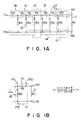
- Fig. 1A is a circuit diagram of the network.
- the trimming resistor network is a two-terminal circuit having first external connection terminal T1 and second external connection terminal T2, and first resistor 11 (which is referred to as R1 and the resistance thereof is r1) is connected to the last stage of the network. Two ends of resistor R1 are respectively connected to terminals T1 and T2 via the first and second coupling bodies.
- each unit stage is formed of inverted L-shaped resistor 17 (surrounded by broken lines) which is constituted by connecting one end of first series resistor 12 (resistor R2 with resistance r2) to one end of parallel trimming resistor 15 (resistor R3 with resistance r3).
- a plurality of stages (six stages in Fig.
- resistors 17 are cascade-connected.
- the other end of resistor R2 is used as third connection terminal 17a
- the other end of resistor R3 is used as fourth connection terminal 17b
- the connection node between resistors R2 and R3 is used as fifth connection terminal 17c.
- third connection terminal 17a of inverted L-shaped resistor 17 is connected to connection terminal 11a of resistor R1.
- Fourth connection terminal 17b is connected to terminal T2 via second coupling body 14 and to second connection terminal 11b of resistor R1.
- Second series resistor 18 (resistor R4 with resistance r4) is connected between terminal T1 and fifth connection terminal 17c of first stage resistor 17.
- Combined resistance r when viewing resistor R1 from the fourth and fifth connection terminals is designed to be equal to r1. That is, r1, r2 and r3 are set to satisfy the following equation.
- resistors attached with marks x are the trimming resistors, which can be cut off by the trimming operation.
- the combined resistance between terminals T1 and T2 in the trimming resistor network of the above construction increases by substantially constant value r2 each time the parallel trimming resistors are sequentially cut off starting from that trimming resistor which is near terminals T1 and T2 towards the first resistor.
- the combined resistance can be changed from the initial value (r4+r1) to the final value (r4+r1+6r2).
- resistor R2 determines constant variation value r2 of the combined resistance, and the number of inverted L-shaped resistors determines the entire range of the resistance variation.
- resistor R4 determines the initial value of the combined resistance and can be omitted when the function of the network of this invention is limited to the resistance adjusting function.
- the resistances of resistors R1 and R3 must be set to satisfy equation (1).
- r2 is previously determined, one of r1 and r3 or ratio r1/r3 can be freely determined. Therefore, r1 and r3 can be determined by taking the design condition and manufacturing condition into consideration so that the occupied area of the network can be suppressed to a minimum, for example.
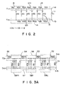
- the trimming resistor network shown in Fig. 2 is obtained by distributing part of resistors R2 of first series resistor 12 in the network of Fig. 1A to the second coupling body. That is, second coupling body 14 includes series-connected resistors via which second external connection terminal T2 is connected to second connection terminal 11b of first resistor 11.
- the same reference numerals as those in Fig. 1A are used to denote the same or similar parts shown in Fig. 1A, and the functions thereof are almost the same as those in Fig. 1A and the explanation thereof is omitted here.
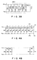
- Fig. 3A is a circuit diagram showing another example of the trimming resistor network of this invention.
- the network is a two-terminal network having first external connection terminal T3 and second external connection terminal T4.
- First resistor 51 (resistor R51 with resistance r51) is connected to the last stage of the network.
- First connection terminal 51a of resistor R51 is connected to terminal T3 via first coupling body 56 which includes first series resistor 52 (resistor R2q with resistance r2q), second series resistor 53 (resistor R2n with resistance r2n), third series resistor 54 (resistor R2m with resistance r2m) and fourth series resistor 55 (resistor R21 with resistance r21).
- Second connection terminal 51b of resistor 51 is connected to terminal T4 via second coupling body 57.
- parallel trimming resistor groups 58m, 58n and 58q are connected between second coupling body 57 and respective points of first coupling body 56.
- parallel trimming resistor group 58m includes m parallel trimming resistors R31, R32, ..., and R3m connected in parallel.
- the combined resistance between terminals T5 and T6 increases stepwise by constant value ro.
- resistances r31, r32, r33, ..., r3m of respective resistors R31, R32, R33, ..., R3m are set to (1 ⁇ 2)ro, (2 ⁇ 3)ro, (3 ⁇ 4)ro, ..., m ⁇ (m+1)ro.
- resistance r2m of resistor R2m is set to mro.
- resistances of the respective resistors in parallel trimming resistor group 58n and resistor R2n, and those of the respective resistors in parallel trimming resistor group 58q and resistor R2q are determined in the same manner as described above. In this case, n or q must be used instead of m.
- Resistance r51 of resistor R51 is set to constant resistance variation ro. In practice, resistors R2q and R51 may be formed of a single resistor R51 with a resistance of (r2q+ro).
- the combined resistance between terminals T3 and T4 is increased by constant value ro each time the parallel trimming resistors are sequentially cut off starting from that trimming resistor which lies near terminals T3 and T4 towards first resistor 51.
- the combined resistance can be changed from the initial value (r21+ro) to the final value ⁇ r21+ro+(m+n+q)ro ⁇ by a stepwise variation of ro.
- the resistance of resistor R2m is set to be equal to total amount mro of increase in the combined resistance which is obtained when the resistors of the preceding parallel trimming resistor group are cut off.
- the resistance of resistor R2m is added to resistor R21. Therefore, the design condition for the succeeding resistor group 58n can be set to be substantially the same as that for the first stage resistor group 58m. This applies to resistors R2n and R2q.
- m, n and q are set to 1, 2 or 3, and the resistances of the parallel trimming resistors of the trimming resistor network are respectively set 2ro, 6ro and 12ro, for example.
- the resistance of first resistor 51 is determined by resistance variation unit ro, and resistor R21 determines the initial value of the combined resistance of the resistor network but can be omitted as required.
- resistors R21, R2m it is possible to distribute part of resistors R21, R2m to R2q of first coupling body 56 in corresponding portions of second coupling body 57.
- three stages of resistor groups 58m, 58n and 58q are used, but the number of the stages of the resistor groups can be selectively set.
- the parallel trimming resistors are formed of resistor films of polysilicon films doped with impurity or nichrome-series alloy films whose heat conductivity is smaller than the metal of the conventional short bar. Therefore, it is possible to use a low power laser beam and reduce the possibility of destroying the underlying layer in the cut-off process.
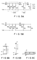
- Fig. 4A is a circuit diagram showing one embodiment of the trimming resistor network shown in Fig. 1A.
- the same reference numerals as are used in Fig. 1A denote the same or similar portions and the explanation thereof is omitted.
- the resistance is adjusted in 1 ⁇ steps from 1 ⁇ to 10 ⁇ .
- the network is connected in series with a resistor (not shown) to be adjusted and is used to set the resistance of the resistor to a desired value. Therefore, resistor R4 used in Fig. 1A to determine the initial value is omitted. Since the resistance variation unit is 1 ⁇ , r2 is set at 1 ⁇ .
- the combined resistance, viewing from connection terminals 17c and 17b of the final stage inverted L-shaped resistor (the right side in Fig. 4A) to the side of resistor R1, is set to 1 ⁇ . That is, a circuit obtained by connecting a resistor (R1) of 1 ⁇ to the final stage inverted L-shaped resistor becomes equal to a resistor of 1 ⁇ . Thus, the equivalent resistor of 1 ⁇ is connected to the eighth inverted L-shaped resistor. As a result, the combined resistances between terminals T1 and T2 in the networks shown in Figs. 4A and 4B are equivalent to each other.
- the same consideration of attaining the equivalent circuit can be applied to the preceding stage towards the first stage. Therefore, the resistance when viewed from left to right from terminals 17c and 17b in each stage of the inverted L-shaped resistor becomes 1 ⁇ , and thus the combined resistance between terminals T1 and T2 is 1 ⁇ .
- the combined resistance between terminals T1 and T2 becomes equal to the sum of 1 ⁇ of the first stage resistor R2 and a resistance of 1 ⁇ obtained from the next stage resistor, as viewed from left to right from connection terminals 17c and 17b, that is, 2 ⁇ .
- 1 ⁇ of the preceding resistor R2 is added so that the resistance between terminals T1 and T2 can be changed from 1 ⁇ to 10 ⁇ in 1 ⁇ steps.
- the embodiment of the trimming resistor network shown in Fig. 3A is explained with reference to Fig. 5A.
- the same reference numerals as used in Fig. 3A denote the same or similar portions and the explanation thereof is omitted.
- the combined resistance between terminals T3 and T4 can be chanted from 2 ⁇ to 6 ⁇ in 1 ⁇ steps.
- the total number (m + n + q) of parallel trimming resistors is 4 and variation unit ro is 1 ⁇ .
- m, n and q are respectively set to 3, 1 and 0 by considering the design and manufacturing conditions.
- r51 of first resistor R51 is set to be equal to variation unit ro, that is, 1 ⁇ . Since initial resistance (r21 + ro) is 2 ⁇ , r21 is 1 ⁇ .
- the initial combined resistance between terminals T3 and T4 of the network with the construction shown in Fig. 5A is 2 ⁇ .
- the parallel trimming resistors are sequentially out off one by one from that one which is to the right of terminals T3 and T4, from left to right in the drawing, the combined resistance between terminals T3 and T4 is changed in 1 ⁇ steps until the final resistance of 6 ⁇ is obtained.
- the number of stages of the parallel trimming resistor groups and the number of parallel trimming resistors constituting the parallel trimming resistor group can be selectively set by considering the design and manufacturing conditions. Therefore, a large degree of freedom can be attained.
- the resistor used in this invention is formed of a thin or thick film, and the resistance of the film resistor is determined by resistivity ⁇ ( ⁇ cm), film thickness t, film length l and film width w of film 4 as shown in Fig. 6A. It is a common practice to obtain desired resistances of resistor films by setting ⁇ and t to preset values and changing l and w. In this case, a high resistance film can be obtained by increasing l and reducing w as shown in Fig. 6B. At this time, w has a lower limitation due to the fine pattern technique. Therefore, in order to form a higher resistance film, it is necessary to further increase l. However, increase in l necessitates a large occupied area for formation of the resistor film.
- a low resistance film can be formed by reducing l and increasing w as shown in Fig. 6C.
- l has a lower limitation due to the fine pattern technique. Therefore, in order to form a lower resistance film, it is necessary to further increase w. However, increase in w necessitates a large occupied area for formation of the resistor film. Therefore, in determining the shape and dimensions of the film resistor, it is necessary to consider the design and manufacturing conditions and the like.
- a degree of freedom for determination of the resistances of resistors for attaining a desired resistance variation is large and therefore the occupied area required for forming the network can be reduced.
- the parallel trimming resistors in the above embodiment are formed of polysilicon films doped with impurity and can be selectively cut off by application of a laser beam. Therefore, the possibility of damaging the underlying layer the time of cutting-off operation by the laser beam can be significantly reduced in comparison with the conventional case wherein metal such as Al with high heat conductivity is cut off.
- the same effect can be obtained by using one of a nichrome-series alloy film, tantalum-series metal film, polyimide organic film, acrylonitrile organic film and ruthenium-series oxide film which have lower heat conductivity that a metal such as Al.
- Fig. 10 is a circuit diagram generally showing in a 4-terminal network form a trimming resistor network of this invention.
- Fig. 11A-11K respectively show the contents of 4-terminal network blocks in Fig. 10.
- 4-terminal network block A in Fig. 10 can have the circuit of Fig. 11A, for example.
- a pure resistor R4 is used as impedance element Z1 and resistor R4 of Fig. 1A or Fig. 2 constitutes 4-terminals network block A.
- each of 4-terminal network blocks Bl-Bi in Fig. 10 can have the circuit of Fig. 11F.
- Pure resistor R3 and R2 (or R2a) are used as impedance elements Z10 and Z11, respectively, and resistors R3 and R2 in Fig. 1A or resistors R3 and R2a in Fig. 2 constitute 4-terminal network block Bl-Bi.
- each 4-terminal network block in Fig. 10 can be constituted by an optimal combination of the circuits of Fig. 11A-11K.
- Fig. 12 shows the contents of impedance elements Z1-Z33 in Fig. 11A-11K.
- Fig. 12 shows a pure resistor (linear element) Ra only.
- the circuit in Fig. 12 is used as the impedance element in respective 4-terminal network blocks A and Bl-Bi, and each of these networks can be constituted by any combination of Fig. 11A-11K.
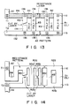
- Fig. 13 shows an arrangement of the resistor network of, for example, Fig. 1A, which is formed in an IC.
- resistor layer 130 is formed by a diffusion.
- Al wiring layer 132 is formed on the substrate in parallel to diffusion resistor layer 130.
- Layers 130 and 132 are bridged like a ladder, via doped polysilicon resistor layers 134-1 to 134-i, to which high-concentration impurities are doped.
- Respective polysilicon resistor layers 134-1 to 134-i are electrically connected to layers 130 and 132, via contacts 136. both ends of layers 130 and 132 are terminated by polysilicon resistor layer R1, via contacts 11a and 11b.
- the materials used for layers 130, 132, and 134 are different from one another. However, the same material can be used for all these layers. For instance, all of layers 130, 132, and 134 can be high-impurity-concentration doped polysilicon resistor layers or a metal resistor film of tantalum or the like. In this case, contacts 136 in Fig. 13 may be omitted.
- the resistor network of Fig.2 can be suitably constituted by the configuration in which the same material is used for all layers 130, 132, and 134. (Incidentally, the resistor network of Fig.
- Fig. 14 shows a configuration in which the resistor network of, e.g. Fig. 2, is integrated into an IC by patterning a metal film layer formed on a substrate thereof.
- optimal resistance values can be obtained for resistors R1-R4, by suitably changing widths of the metal resistor patterns.
- Fig. 15 shows a modification of Fig. 14.
- the effective length of a metal resistor film pattern is elongated by intentionally compricating the figure or shape of the pattern.
- relatively high-resistance trimming resistors can be obtained without excessively increasing the pattern area.
- Fig. 16 is a sectional view of a semiconductor substrate in which trimming resistors R2 and/or R3 of Fig. 1A, etc. are formed.
- N+ buried layer 164 is formed at the boundary between P substrate 160 and P- epitaxial layer 162.
- a diffusion layer, doped polysilicon layer, etc. can be used for buried layer 164.
- N type impurities e.g. phosphorus
- N+ layers 166, 164, and 168 are electrically series-connected to form a trimming resistor body.
- N+ layer 166 is connected to Al wiring 170b, via a contact hole, and N+ layer 168 is connected to Al wiring 170c, via anther contact hole.
- Fig. 16 illustrates a case wherein wiring 170a-170b is cut by laser. When no laser cut is effected, wiring 170b continues wiring 170a.
- any circuit element other than a trimming resistor body can be built i the specific area of epitaxial layer 162 surrounded by N+ layers 166, 164, and 168.
- these N+layers can serve not only as trimming resistor but also as element isolation layers with respect to other circuit elements formed in the same substrate.
- the present invention can be suitably used for trimming a resistor array in an A/D converter or an operational amplifier, which is formed in a monolithic IC or in hybrid IC.
- the trimming resistor is formed of a polysilicon film doped with impurity or nichrome-series alloy or the like which has lower heat conductivity than a metal such as Al. Therefore, in cutting off the trimming resistor, the trimming can be effected without destroying the underlying layer.
- a degree of freedom for determination of the resistances of resistors for attaining a desired effect is large and therefore the occupied area required for forming the network can be reduced.
Claims (2)
- Réseau de résistances d'ajustement comprenant des première et seconde bornes de connexion externe (T1, T2) ; une première résistance (R1, 11) ayant deux extrémités servant de première et seconde bornes de connexion (11a, 11b) ; un premier corps de liaison (13) pour connecter la première borne de connexion externe (T1) à la première borne de connexion (11a), par l'intermédiaire de résistances connectées en série (R2, R4) ; un second corps de liaison (14) pour connecter la seconde borne de connexion externe (T2) à la seconde borne de connexion (11b), directement ou par l'intermédiaire de résistances connectées en série (R2b) ; et des résistances d'ajustement parallèles (R3) ayant deux extrémités connectées, respectivement, au premier et au second corps de liaison (13, 14) ; dans lequel la valeur de résistance combinée entre les première et seconde bornes de connexion externe (T1, T2) augmente d'une valeur sensiblement constante chaque fois que l'une des résistances d'ajustement parallèles (R3) est coupée, en partant, de manière séquentielle, de la résistance d'ajustement parallèle (R3) qui est proche des bornes de connexion externe (T1, T2) vers la première résistance (R1, 11).
- Réseau de résistances selon la revendication 1, caractérisé en ce qu'au moins une partie desdites résistances d'ajustement (R3) est formée à partir d'un film choisi dans un groupe constitué d'un film de silicium polycristallin dopé avec une impureté, d'un film d'alliage nichrome série, d'un film métallique de tantale série, d'un film organique à base de polyimide, d'un film organique à base d'acrylonytrile et d'un film d'oxyde de ruthénium série.
Applications Claiming Priority (2)
| Application Number | Priority Date | Filing Date | Title |
|---|---|---|---|
| JP63022804A JPH01199404A (ja) | 1988-02-04 | 1988-02-04 | トリミング抵抗回路網 |
| JP22804/88 | 1988-02-04 |
Publications (3)
| Publication Number | Publication Date |
|---|---|
| EP0327078A2 EP0327078A2 (fr) | 1989-08-09 |
| EP0327078A3 EP0327078A3 (fr) | 1991-04-03 |
| EP0327078B1 true EP0327078B1 (fr) | 1994-08-17 |
Family
ID=12092870
Family Applications (1)
| Application Number | Title | Priority Date | Filing Date |
|---|---|---|---|
| EP89101755A Expired - Lifetime EP0327078B1 (fr) | 1988-02-04 | 1989-02-01 | Réseau de résistances d'équilibrages |
Country Status (4)
| Country | Link |
|---|---|
| US (1) | US4906966A (fr) |
| EP (1) | EP0327078B1 (fr) |
| JP (1) | JPH01199404A (fr) |
| DE (1) | DE68917489T2 (fr) |
Cited By (1)
| Publication number | Priority date | Publication date | Assignee | Title |
|---|---|---|---|---|
| DE102020134776A1 (de) | 2020-12-22 | 2022-06-23 | urbanhive UG (haftungsbeschränkt) | Modulares System für Hydrokulturen für den Einsatz im Innenraum |
Families Citing this family (33)
| Publication number | Priority date | Publication date | Assignee | Title |
|---|---|---|---|---|
| JPH0294555A (ja) * | 1988-09-30 | 1990-04-05 | Toshiba Corp | トリミング抵抗体 |
| JP2664793B2 (ja) * | 1990-04-06 | 1997-10-22 | 株式会社東芝 | 半導体装置の製造方法 |
| US5689428A (en) | 1990-09-28 | 1997-11-18 | Texas Instruments Incorporated | Integrated circuits, transistors, data processing systems, printed wiring boards, digital computers, smart power devices, and processes of manufacture |
| US5099148A (en) * | 1990-10-22 | 1992-03-24 | Sgs-Thomson Microelectronics, Inc. | Integrated circuit having multiple data outputs sharing a resistor network |
| GB2259807B (en) * | 1991-09-23 | 1995-09-06 | Crystal Semiconductor Corp | Low drift resistor structure |
| JP2637662B2 (ja) * | 1992-02-25 | 1997-08-06 | ローム株式会社 | チップ型複合電子部品の製造方法及びチップ型ネットワーク抵抗器の製造方法 |
| US5567550A (en) * | 1993-03-25 | 1996-10-22 | Texas Instruments Incorporated | Method of making a mask for making integrated circuits |
| CA2145697A1 (fr) * | 1994-04-15 | 1995-10-16 | Michael F. Mattes | Methode et dispositif pour corriger l'effet des fluctuations de temperature a l'entree d'un circuit de gain |
| US5507171A (en) * | 1994-04-15 | 1996-04-16 | Ssi Technologies, Inc. | Electronic circuit for a transducer |
| JP3124473B2 (ja) * | 1994-08-19 | 2001-01-15 | セイコーインスツルメンツ株式会社 | 半導体装置とその製造方法 |
| US5640137A (en) * | 1995-01-24 | 1997-06-17 | Zilog, Inc. | Polysilicon resistor cooling |
| DE69531058D1 (de) * | 1995-12-20 | 2003-07-17 | Ibm | Halbleiter IC chip mit elektrisch verstellbaren Widerstandstrukturen |
| TW340944B (en) * | 1996-03-11 | 1998-09-21 | Matsushita Electric Ind Co Ltd | Resistor and method of making the same |
| DE19743271C1 (de) | 1997-09-30 | 1998-10-29 | Siemens Ag | Lineare Anordnung metallischer Sicherungsstrecken auf Wafern, wobei durch "Schießen" der Sicherungsstrecken Schaltungskenngrößen einstellbar sind |
| US6664500B2 (en) * | 2000-12-16 | 2003-12-16 | Anadigics, Inc. | Laser-trimmable digital resistor |
| US20030011625A1 (en) * | 2001-07-13 | 2003-01-16 | Kellis James T. | Brightness control of displays using exponential current source |
| DE10224180B4 (de) * | 2002-05-31 | 2007-01-04 | Infineon Technologies Ag | Schaltungsanordnung zur Einstellung des Eingangswiderstandes und der Eingangskapazität eines integrierten Halbleiterschaltungschips |
| JP2005158936A (ja) * | 2003-11-25 | 2005-06-16 | Sharp Corp | 調整インピーダンス素子、半導体装置及びトリミング方法 |
| US7300807B2 (en) * | 2004-04-14 | 2007-11-27 | International Business Machines Corporation | Structure and method for providing precision passive elements |
| JP4508023B2 (ja) * | 2005-07-21 | 2010-07-21 | 株式会社デンソー | レーザトリミング評価方法およびレーザトリミング用レーザ強度設定方法 |
| TWI285068B (en) | 2006-03-24 | 2007-08-01 | Ind Tech Res Inst | An adjustable resistor embedded in a multi-layer substrate and method for forming the same |
| CN102438400A (zh) * | 2006-03-31 | 2012-05-02 | 财团法人工业技术研究院 | 多层基板内的可调电阻及其形成方法 |
| DE102006052748A1 (de) * | 2006-08-14 | 2008-04-30 | Rohde & Schwarz Gmbh & Co. Kg | Oszilloskop-Tastkopf |
| US8240027B2 (en) * | 2008-01-16 | 2012-08-14 | Endicott Interconnect Technologies, Inc. | Method of making circuitized substrates having film resistors as part thereof |
| US8338192B2 (en) * | 2008-05-13 | 2012-12-25 | Stmicroelectronics, Inc. | High precision semiconductor chip and a method to construct the semiconductor chip |
| KR20090121470A (ko) * | 2008-05-22 | 2009-11-26 | 주식회사 하이닉스반도체 | 임피던스 교정 회로를 포함하는 반도체 메모리 장치 |
| WO2010035608A1 (fr) * | 2008-09-25 | 2010-04-01 | Semiconductor Energy Laboratory Co., Ltd. | Dispositif à semi-conducteurs et son procédé de fabrication |
| DE112011105993T5 (de) | 2011-12-23 | 2014-09-04 | Intel Corporation | Prozessabstimmbarer Widerstand mit Nutzerwählbaren Werten |
| JP6357298B2 (ja) * | 2012-05-02 | 2018-07-11 | 株式会社半導体エネルギー研究所 | トリミング抵抗 |
| US9634646B1 (en) | 2015-10-27 | 2017-04-25 | Analog Devices, Inc. | Mismatch calibration of capacitive differential isolator |
| JP2017146134A (ja) * | 2016-02-16 | 2017-08-24 | アルプス電気株式会社 | 抵抗値調整回路および荷重検出装置ならびに抵抗値調整方法 |
| US11056253B2 (en) * | 2019-03-18 | 2021-07-06 | Qualcomm Incorporated | Thin-film resistors with flexible terminal placement for area saving |
| US10653013B1 (en) * | 2019-09-03 | 2020-05-12 | The Boeing Company | Thin film resistor having surface mounted trimming bridges for incrementally tuning resistance |
Family Cites Families (9)
| Publication number | Priority date | Publication date | Assignee | Title |
|---|---|---|---|---|
| GB732437A (en) * | 1951-10-03 | 1955-06-22 | Technograph Printed Circuits L | Electric circuit components |
| US3431640A (en) * | 1966-03-04 | 1969-03-11 | Burroughs Corp | Method for adjusting thin film resistors |
| US3916142A (en) * | 1973-03-29 | 1975-10-28 | Gte Automatic Electric Lab Inc | Method of static trimming of film deposited resistors |
| FI52780C (fi) * | 1974-06-18 | 1977-11-10 | Paramic Ab Oy | Vastusarvoltaan aseteltava vastusverkko. |
| US4150366A (en) * | 1976-09-01 | 1979-04-17 | Motorola, Inc. | Trim network for monolithic circuits and use in trimming a d/a converter |
| US4338590A (en) * | 1980-01-07 | 1982-07-06 | National Semiconductor Corporation | Multi stage resistive ladder network having extra stages for trimming |
| JPS56132815A (en) * | 1980-03-21 | 1981-10-17 | Nec Corp | Reference step voltage generating circuit |
| JPS60160726A (ja) * | 1984-02-01 | 1985-08-22 | Fujitsu Ltd | Cmos駆動回路 |
| US4647906A (en) * | 1985-06-28 | 1987-03-03 | Burr-Brown Corporation | Low cost digital-to-analog converter with high precision feedback resistor and output amplifier |
-
1988
- 1988-02-04 JP JP63022804A patent/JPH01199404A/ja active Granted
-
1989
- 1989-02-01 DE DE68917489T patent/DE68917489T2/de not_active Expired - Fee Related
- 1989-02-01 EP EP89101755A patent/EP0327078B1/fr not_active Expired - Lifetime
- 1989-02-03 US US07/305,811 patent/US4906966A/en not_active Expired - Lifetime
Non-Patent Citations (1)
| Title |
|---|
| & JP-A-60 160726 (FUJITSU) 22 August 1985, * |
Cited By (3)
| Publication number | Priority date | Publication date | Assignee | Title |
|---|---|---|---|---|
| DE102020134776A1 (de) | 2020-12-22 | 2022-06-23 | urbanhive UG (haftungsbeschränkt) | Modulares System für Hydrokulturen für den Einsatz im Innenraum |
| WO2022136530A1 (fr) | 2020-12-22 | 2022-06-30 | urbanhive UG (haftungsbeschränkt) | Système modulaire pour culture hydroponique pour une utilisation en intérieur |
| DE102020134776B4 (de) | 2020-12-22 | 2023-05-25 | urbanhive GmbH | Modulares System für Hydrokulturen für den Einsatz im Innenraum |
Also Published As
| Publication number | Publication date |
|---|---|
| US4906966A (en) | 1990-03-06 |
| EP0327078A2 (fr) | 1989-08-09 |
| JPH01199404A (ja) | 1989-08-10 |
| DE68917489D1 (de) | 1994-09-22 |
| JPH0552043B2 (fr) | 1993-08-04 |
| DE68917489T2 (de) | 1994-12-15 |
| EP0327078A3 (fr) | 1991-04-03 |
Similar Documents
| Publication | Publication Date | Title |
|---|---|---|
| EP0327078B1 (fr) | Réseau de résistances d'équilibrages | |
| EP0450648B1 (fr) | Dispositif à semi-conducteur dont les caractéristiques de sortie sont ajustables par adaptation en fonction | |
| JP2945166B2 (ja) | 電気抵抗体およびその製造方法 | |
| EP0361439B1 (fr) | Elément résistif ajustable pour circuit microélectronique | |
| KR920003467B1 (ko) | 트리밍소자와 그 전기단락방법 | |
| EP0544364A2 (fr) | Dispositif semi-conducteur monolithique à structure verticale comprenant un transistor de puissance à base profonde et doigts d'émetteur avec résistance de ballast | |
| US20030154456A1 (en) | Resistor circuit | |
| US4528546A (en) | High power thick film | |
| US7205880B2 (en) | Trimmer impedance component, semiconductor device and trimming method | |
| US5257005A (en) | Small value precision integrated circuit resistors | |
| US6674316B2 (en) | Methods and apparatus for trimming electrical devices | |
| KR920003074Y1 (ko) | 트리밍 저항회로망 | |
| JPH08195479A (ja) | 半導体装置及びその製造方法 | |
| US3906430A (en) | Matrix resistors for integrated circuit | |
| KR920003703B1 (ko) | 반도체 장치 | |
| EP0024923A1 (fr) | Structure de transistor | |
| JPS63310160A (ja) | レ−ザ−トリミング方法 | |
| JPS6041261A (ja) | 半導体パワ−部品及びその製造方法 | |
| JPH09232117A (ja) | 半導体装置 | |
| JP3476414B2 (ja) | 半導体装置 | |
| JPH07211867A (ja) | 抵抗素子 | |
| JP2701672B2 (ja) | トリミング用抵抗器 | |
| JPH0964277A (ja) | 抵抗素子及びその製造方法 | |
| JPS61180469A (ja) | 半導体分布インピ−ダンス装置 | |
| JPH08124707A (ja) | 薄膜チップ抵抗器 |
Legal Events
| Date | Code | Title | Description |
|---|---|---|---|
| PUAI | Public reference made under article 153(3) epc to a published international application that has entered the european phase |
Free format text: ORIGINAL CODE: 0009012 |
|
| 17P | Request for examination filed |
Effective date: 19890224 |
|
| AK | Designated contracting states |
Kind code of ref document: A2 Designated state(s): DE FR GB |
|
| PUAL | Search report despatched |
Free format text: ORIGINAL CODE: 0009013 |
|
| RHK1 | Main classification (correction) |
Ipc: H01C 17/22 |
|
| AK | Designated contracting states |
Kind code of ref document: A3 Designated state(s): DE FR GB |
|
| 17Q | First examination report despatched |
Effective date: 19930201 |
|
| GRAA | (expected) grant |
Free format text: ORIGINAL CODE: 0009210 |
|
| AK | Designated contracting states |
Kind code of ref document: B1 Designated state(s): DE FR GB |
|
| REF | Corresponds to: |
Ref document number: 68917489 Country of ref document: DE Date of ref document: 19940922 |
|
| ET | Fr: translation filed | ||
| PLBE | No opposition filed within time limit |
Free format text: ORIGINAL CODE: 0009261 |
|
| STAA | Information on the status of an ep patent application or granted ep patent |
Free format text: STATUS: NO OPPOSITION FILED WITHIN TIME LIMIT |
|
| 26N | No opposition filed | ||
| PGFP | Annual fee paid to national office [announced via postgrant information from national office to epo] |
Ref country code: DE Payment date: 19970207 Year of fee payment: 9 |
|
| PGFP | Annual fee paid to national office [announced via postgrant information from national office to epo] |
Ref country code: FR Payment date: 19970211 Year of fee payment: 9 |
|
| PG25 | Lapsed in a contracting state [announced via postgrant information from national office to epo] |
Ref country code: FR Free format text: THE PATENT HAS BEEN ANNULLED BY A DECISION OF A NATIONAL AUTHORITY Effective date: 19980228 |
|
| REG | Reference to a national code |
Ref country code: GB Ref legal event code: 746 Effective date: 19981007 |
|
| PG25 | Lapsed in a contracting state [announced via postgrant information from national office to epo] |
Ref country code: DE Free format text: LAPSE BECAUSE OF NON-PAYMENT OF DUE FEES Effective date: 19981103 |
|
| REG | Reference to a national code |
Ref country code: FR Ref legal event code: ST |
|
| REG | Reference to a national code |
Ref country code: GB Ref legal event code: IF02 |
|
| PGFP | Annual fee paid to national office [announced via postgrant information from national office to epo] |
Ref country code: GB Payment date: 20060201 Year of fee payment: 18 |
|
| GBPC | Gb: european patent ceased through non-payment of renewal fee |
Effective date: 20070201 |
|
| PG25 | Lapsed in a contracting state [announced via postgrant information from national office to epo] |
Ref country code: GB Free format text: LAPSE BECAUSE OF NON-PAYMENT OF DUE FEES Effective date: 20070201 |