EP0308018B1 - Ablenkschaltung mit Korrektur der N-S-Kissenverzerrung - Google Patents
Ablenkschaltung mit Korrektur der N-S-Kissenverzerrung Download PDFInfo
- Publication number
- EP0308018B1 EP0308018B1 EP88201972A EP88201972A EP0308018B1 EP 0308018 B1 EP0308018 B1 EP 0308018B1 EP 88201972 A EP88201972 A EP 88201972A EP 88201972 A EP88201972 A EP 88201972A EP 0308018 B1 EP0308018 B1 EP 0308018B1
- Authority
- EP
- European Patent Office
- Prior art keywords
- voltage
- vertical
- current
- rate
- envelope
- Prior art date
- Legal status (The legal status is an assumption and is not a legal conclusion. Google has not performed a legal analysis and makes no representation as to the accuracy of the status listed.)
- Expired - Lifetime
Links
- 241000226585 Antennaria plantaginifolia Species 0.000 title claims abstract description 37
- 238000004804 winding Methods 0.000 claims abstract description 41
- 239000003990 capacitor Substances 0.000 description 23
- 230000007423 decrease Effects 0.000 description 11
- 230000007704 transition Effects 0.000 description 10
- 230000003534 oscillatory effect Effects 0.000 description 9
- 230000005284 excitation Effects 0.000 description 7
- 230000001965 increasing effect Effects 0.000 description 7
- 230000008878 coupling Effects 0.000 description 4
- 238000010168 coupling process Methods 0.000 description 4
- 238000005859 coupling reaction Methods 0.000 description 4
- 230000003247 decreasing effect Effects 0.000 description 4
- 230000010355 oscillation Effects 0.000 description 4
- 230000008859 change Effects 0.000 description 3
- 238000005070 sampling Methods 0.000 description 3
- 230000003111 delayed effect Effects 0.000 description 2
- 230000000694 effects Effects 0.000 description 2
- 230000000670 limiting effect Effects 0.000 description 2
- 230000004048 modification Effects 0.000 description 2
- 238000012986 modification Methods 0.000 description 2
- 230000002441 reversible effect Effects 0.000 description 2
- 229920006395 saturated elastomer Polymers 0.000 description 2
- OAICVXFJPJFONN-UHFFFAOYSA-N Phosphorus Chemical compound [P] OAICVXFJPJFONN-UHFFFAOYSA-N 0.000 description 1
- 240000000136 Scabiosa atropurpurea Species 0.000 description 1
- 230000009471 action Effects 0.000 description 1
- 230000009286 beneficial effect Effects 0.000 description 1
- 230000007850 degeneration Effects 0.000 description 1
- 230000001419 dependent effect Effects 0.000 description 1
- 230000004069 differentiation Effects 0.000 description 1
- 238000010894 electron beam technology Methods 0.000 description 1
- 238000001914 filtration Methods 0.000 description 1
- 230000001939 inductive effect Effects 0.000 description 1
- 230000010363 phase shift Effects 0.000 description 1
- 238000007493 shaping process Methods 0.000 description 1
Images


Classifications
-
- H—ELECTRICITY
- H04—ELECTRIC COMMUNICATION TECHNIQUE
- H04N—PICTORIAL COMMUNICATION, e.g. TELEVISION
- H04N3/00—Scanning details of television systems; Combination thereof with generation of supply voltages
- H04N3/10—Scanning details of television systems; Combination thereof with generation of supply voltages by means not exclusively optical-mechanical
- H04N3/16—Scanning details of television systems; Combination thereof with generation of supply voltages by means not exclusively optical-mechanical by deflecting electron beam in cathode-ray tube, e.g. scanning corrections
- H04N3/22—Circuits for controlling dimensions, shape or centering of picture on screen
- H04N3/23—Distortion correction, e.g. for pincushion distortion correction, S-correction
- H04N3/233—Distortion correction, e.g. for pincushion distortion correction, S-correction using active elements
Definitions
- This invention relates to north-south pin-cushion corrected deflection circuits.
- US-A-3748531 concerns compensating for beam-spot distortion in the corners of a color picture display apparatus.
- the distortion may be so severe as to produce color superposition errors.
- US-A-3748531 provides a circuit arrangement for generating by means of a modulator in a color picture display device a sawtooth correction current of line frequency flowing through the line deflection coils and having an amplitude varying at field frequency for the purpose of obtaining a better color superposition in the corners of the screen of the display tube.
- the arrangement comprises means to add an additional correction current which flows in the same direction as the first mentioned current and which is proportional to the third power of both the line and the field deflection currents.
- Said means may be a saturable coil or a resonant circuit which is tuned to a frequency which lies between the like frequency and twice the value thereof. In the latter case the voltage present across the circuit may be used for correcting the north/south pincushion distortion.
- the modulator is controlled by an amplifier comprising a linear and a voltage-dependent resistor which ensure that a third-power component is added also to said field deflection current.
- Picture tubes for video apparatus such as television receivers or computer monitors may require modulation of the field deflection current for correcting a geometrical distortion known as north-south pincushion distortion.
- a cause of this distortion is the difference between the beam scanning radius of curvature and the tube faceplate radius of curvature.
- New, flatter faceplate picture tubes having aspherical faceplate curvatures require a more complex form of north-south pincushion correction than is provided for a conventional spherical faceplate picture tube.
- a tube of the type having a complex curvature faceplate is described in US-A-4786840 in the name of F.R. Ragland, Jr. and entitled CATHODE-RAY TUBE HAVING A FACEPLATE PANEL WITH A SUBSTANTIALLY PLANAR PERIPHERY, corresponding to UK published application GB-A-2136198A, published 12 September 1984.
- a television display apparatus that provides for raster scanning of a picture tube which includes an aspherical faceplate of relatively flat contour, a north-south pincushion correction circuit comprising: a field deflection winding; a field deflection amplifier for generating field deflection current in said field deflection winding; means for producing line rate modulation of said field deflection current; and means for varying at a field rate the envelope of the line rate modulation of said field deflection current; characterized by means for nonlinearly waveshaping said envelope to provide a north-south pincushion corrected field deflection current that includes correction of remaining north-south pincushion distortion associated with raster-scanning in conjunction with said picture tube.
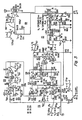
- a vertical deflection circuit 20 includes a vertical deflection amplifier 21 coupled to a vertical deflection winding L V for generating a vertical deflection current i V in the deflection winding.
- Vertical deflection current i V flows to ground via an LC resonant circuit 22 or tank circuit of a north-south pincushion correction circuit 23 embodying the invention, via a coupling capacitor C V and via a sampling resistor R s .
- the vertical rate sawtooth voltage 24 developed by the deflection current i V in sampling resistor R s provides negative feedback for vertical deflection amplifier 21.
- Horizontal deflection current is generated in horizontal deflection winding L H of FIGURE 2 by a horizontal deflection circuit 19.
- Vertical deflection current is generated in vertical deflection winding L V of FIGURE 2 by a vertical deflection circuit 220, that comprises either the circuit 20 of FIGURE 1 or the circuit 120 of FIGURE 3, to be discussed later.
- North-south pincushion distortion of a raster being displayed on the screen of a square-planar picture tube may be corrected, by means of a line rate, cosine current which is added to the field deflection current.
- the cosine correction current in addition to substantially correcting north-south pincushion geometric error, provides a better fit for a residual line frequency distortion of the raster, such as gullwing distortion, caused by the nonspherical nature of the faceplate of a square-planar picture tube.
- gullwing distortion such as gullwing distortion
- the cosine function corrects most of this residual error because of the change in polarity of slope of the cosine current at each zero crossing.
- a parabolically shaped line rate correction is less beneficial than a cosinusoidally shaped correction because of the presence of gullwing distortion.
- LC resonant circuit 22 of FIGURE 1 is excited at a line rate by a switching amplifier, Darlington transistor Q4.
- LC resonant circuit 22 is tuned to the horizontal deflection frequency.
- a line rate cosinusoidal circulating current i1 is thereby generated in resonant circuit 22.
- a control circuit 26 develops a control signal 33H that switches conductive levels of amplifier Q4 at a line rate. The switching occurs with a substantially 50% duty cycle.
- the 50% duty cycle of control signal 33H is advantageous when exciting LC resonant circuit 22 at its natural frequency f H . Because the strongest frequency component of the 50% duty cycle signal is the fundamental frequency, f H , little harmonic distortion is introduced into the excitation of LC resonant circuit 22.
- control circuit 26 switches conductive levels of switching amplifier Q4 at a line rate between first and second levels of conduction. To produce a vertical rate variation of the amplitude of cosine correction current i1, the magnitudes of the two conduction levels are varied at a vertical rate in a sawtooth manner.
- the envelope of the line rate modulation of the vertical deflection current i V is of maximum height at the top and bottom of the raster and minimum at the center, thereby providing the proper amount of north-south pincushion correction at all times during vertical scan.
- Control circuit 26 includes first and second control amplifiers Q1 and Q2, differentially connected, for generating first and second control currents i Q1 and i Q2 at the respective collector outputs of transistors Q1 and Q2.
- the collector outputs of control amplifiers Q1 and Q2 are switched to ground at a line rate by respective first and second control switches, QA and QB.
- Horizontal retrace pulse voltage 31 is integrated by a resistor R1 and a capacitor C1 into a horizontal sawtooth voltage 32, identified as the voltage V hs in FIGURE 4b.
- Horizontal sawtooth voltage 32 is applied to the inverting input terminal of switch QA and to the noninverting input terminal of switch QB.
- the other input terminals of switches QA and QB are grounded.
- control switches QA and QB are switched between conductive and nonconductive states at a line rate in phase opposition to each other.
- switch QA is in saturated conduction and switching voltage 27H is at ground potential.
- control switch QB is cutoff and switching voltage 28H is at the voltage level of the collector of control amplifier Q2.
- control switch QA is cutoff and control switch QB is in saturated conduction.
- Switching voltage 28H is at ground potential and switching voltage 27H is at the voltage level of the collector of control amplifier Q1.
- the line rate, switching voltages 27H and 28H are superimposed at the base of a driver transistor Q3 via diodes D1 and D2.
- Transistor Q3 is arranged in an emitter-follower configuration
- the emitter output electrode of driver transistor Q3 is AC coupled to the base of power switching amplifier Q4 via a capacitor C3.
- Transistor Q4 may be operated in the linear mode.
- DC bias for the base of transistor Q4 is provided by voltage dividing resistors R15 and R16.
- Emitter degeneration is provided by a resistor R17.
- Line rate voltages 27H and 28H at the base of driver transistor Q3 produces a bilevel, line rate control voltage 33H at the output emitter electrode of transistor Q3 having first and second voltage levels 33a and 33b, as illustrated in FIGURE 4e.
- Voltage level 33a is directly related to the amplitude of switching voltage 27H.
- Voltage level 33b is directly related to the amplitude of switching voltage 28H.
- Bilevel control signal 33H switches conductive levels of output switching amplifier Q4 at a line rate between first and second levels of conduction.
- the collector current i Q4 of transistor Q4 is a bilevel current having a first current level 34a that is directly related to the magnitude of level 33a of control signal 33H and having a second current level 34b that is directly related to the magnitude of level 33b.
- Line rate output current i Q4 excites LC resonant circuit 22 into a substantially cosinusoidal oscillation.
- the capacitive branch of resonant circuit 22 comprises a capacitor C5 coupled across the secondary winding W s of an adjustable transformer T1.
- Transformer T1 comprises the inductive branch of resonant circuit 22.
- the primary winding W p of transformer T1 is coupled to the collector output electrode of switching amplifier Q4.
- Transformer T1 is tuned to resonate at the horizontal deflection frequency.
- FIGURES 5b and 5c illustrate the cosinusoidal correction current i1 in secondary winding W s and the 90° phase-shifted voltage V1 across resonant tank circuit 22.
- FIGURE 5a illustrates a reference horizontal retrace pulse voltage.
- an oscillatory waveform is considered cosinusoidal when the maxima or minima occur at the center of horizontal trace or retrace and is considered sinusoidal when zero at those instants.
- Voltage V1 generates in vertical deflection winding L v a cosinusoidal correction current component to correct north-south pincusion error.
- This component is phased by correction current i1 of LC resonant circuit 22 and has an amplitude of i1L Ws /L V , where L Ws is the inductance of the secondary winding W s of transformer T1.
- the correction current component of vertical deflection current i V provides a line rate modulation which adds to the vertical deflection current at the center of each line scan and which subtracts at the beginning and end of each line scan.
- Winding W p represents to transistor Q4 a high load impedance at the resonance frequency of resonant circuit 22. At all other frequencies, the impedance of winding W p is low. Harmonics of the line frequency are therefore short-circuited by winding W p .
- the inductance of transformer T1 is adjustable for controlling the phase of the line rate modulation of the field deflection current to avoid north-south trapeze distortion. For correct phasing of the line rate modulation, as will be explained later, it is also advantageous that the switching of control signal 33H between levels 33a and 33b occurs at the center of horizontal retrace, at time t2 of FIGURES 4a-4g and at the center of horizontal trace, at time t4.
- the amplitude of the cosinusoidal, line rate modulation of the vertical deflection current is varied at a vertical rate in a generally sawtooth manner.
- the envelope height of the amplitude modulation envelope of vertical deflection current i V is maximum at the top and bottom of the raster, at the beginning and end of field scan, and is zero at the center of the raster or field scan.
- the closely spaced vertical lines in the waveform of FIGURE 6a schematically represent the line rate modulation of the vertical deflection current.
- control circuit 26 varies both level 33a and level 33b of control signal 33H at a field rate.
- level 33a varies in a sense opposite that of level 33b during field scan, such that, for example, level 33a decreases in magnitude during field scan whereas level 33b increases.
- the phase of the cosinusoidal correction of the vertical deflection current during the second half of vertical scan is phase-shifted by 180° from the cosinusoidal correction provided during the first half of vertical scan.
- control current i Q2 the collector current of transistor Q2
- Control current i Q1 the collector current of transistor Q1
- Control current i Q1 the collector current of transistor Q1
- the amplitudes of switching voltages 27H and 28H also vary at a vertical rate, with the amplitude of switching voltage 27H decreasing during field scan and the amplitude of switching voltage 28H increasing during field scan.
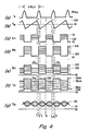
- FIGURES 6b through 6i illustrate various waveforms at an expanded time scale near symmetrically located field scan instants T b and T e of FIGURE 6a.
- Field scan instants T b and T e are equally spaced from instant T c , the center of field scan.
- vertical deflection current i V of FIGURE 6a has the same magnitude I O , but opposite sign, at field scan instants T b and T e .
- Line rate switching voltage 27H of FIGURE 6d is phased to provide a positive going transition at the center of horizontal trace, at time t t of horizontal retrace pulse voltage V r of FIGURE 6b and to provide a negative going transition at the center of horizontal retrace at time t r .
- Voltage 27H maintains the same phase throughout field scan, including instants T b and T e .
- the amplitude of voltage 27H decreases at a vertical rate in a sawtooth manner, from a voltage level V1′ near field scan instant T b , to a voltage level V2′ near field scan instant T e .
- Line rate switching voltage 28H of FIGURE 6e is phased opposite that of voltage 27H, to provide a negative going transition at the center of horizontal trace, at time t t and to provide a positive going transition at the center of horizontal retrace, and time t r .
- Voltage 28H maintains the same phase relationship throughout field scan, including instants T b and T e .
- the amplitude of voltage 28H increases at a vertical rate in a sawtooth manner, from the voltage level V′1, near field scan instant T b , to the voltage level V′2, near field scan instant T e .
- Line rate control voltage 33H equals the superposition of voltages 27H and 28H.
- the amplitude of voltage 27H predominates, and the phase of control voltage 33H equals the phase of voltage 27H, with a positive going transition occurring at the center of horizontal trace.
- the amplitudes of voltages 27H and 28H are equal and control voltage 33H contains no square wave component.
- the amplitude of voltage 28H predominates, and the phase of control voltage 33H switches by 180° to become equal to the phase of voltage 28H, with a negative going transition occurring at the center of horizontal trace.
- control voltage 33H from the first half of field scan to the second half of field scan produces the required phase reversal of the line rate, cosinusoidal correction current component 48 of vertical deflection current i V , illustrated in FIGURE 6c.
- control voltage 33H of FIGURE 6f has a positive going transition at time t t , the center of horizontal trace, thereby producing a positive amplitude correction current component 48p of FIGURE 6c.
- control voltage 33H has a negative going transition at time t t , thereby producing a negative amplitude correction current component 48n.
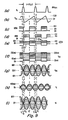
- FIGURE 7a illustrates voltage V Q1 at the collector of control amplifier Q1 in an vertical rate time scale.
- the line rate modulation of collector voltage V Q1 is schematically indicated by the closely spaced vertical lines.
- FIGURE 7b illustrates voltage V Q2 at the collector of amplifier transistor Q2.
- the line rate modulation of collector voltage V Q2 is schematically indicated by the closely spaced vertical lines.
- a comparison of FIGURES 7a and 7b reveals that the vertical rate variation of voltage V Q1 is in an opposite sense to that of the vertical rate variation of the voltage V Q2 .
- FIGURE 7c illustrates voltage V eQ3 at the emitter output of driver transistor Q3, at an expanded time scale relative to the time scale of the other waveforms of FIGURE 7.
- Voltage V eQ3 as represented in FIGURE 7c, corresponds to the vertical rate modulation envelope of control signal 33H.
- the line rate modulation of voltage V eQ3 is schematically indicated in FIGURE 7c by the closely spaced vertical lines.
- the vertical rate varying control voltage V eQ3 is applied to the base of switching amplifier Q4 to vary at a vertical rate the amplitude of exciting current i Q4 .
- the envelope of current i Q4 may be represented by two generally sawtooth lines 36 and 37 varying at a field rate in opposing senses.
- the amplitude of the line rate component of current i Q4 decreases in a generally sawtooth manner from the beginning of field scan to the center of field scan and increases in a generally sawtooth manner from the center of field scan to the end of field scan.
- the vertical rate envelope of collector voltage V Q4 is illustrated in FIGURE 7e and is generally of the same waveshape as that of the collector current i Q4 of FIGURE 7d.
- the crossover point T c of the voltage envelope of FIGURE 7e occurs approximately at the center of vertical trace. Time T c is delayed from the crossover point T i of the current envelope of FIGURE 7d because of crosstalk between horizontal deflection winding L H and vertical deflection winding L V , to be described later.
- the vertical rate modulation of the conduction of switching amplifier Q4 produces a vertical rate modulation of correction current i1 in LC resonant circuit 22 and produces a vertical rate modulation of the amplitude of the oscillatory voltage V1, as illustrated in FIGURES 7f and 7g, respectively.
- the line rate components of current i1 and voltage V1 are schematically indicated in FIGURES 7f and 7g by the closely spaced vertical lines.
- the effect of the vertical rate modulation of current i1 and voltage V1 on vertical deflection current i V is illustrated in FIGURE 6a wherein the envelope of the line rate modulated vertical deflection current produces maximum line rate modulation at the top and bottom of vertical scan and no modulation at the center of vertical scan.
- This crosstalk is in the form of an induced voltage and an induced current in vertical deflection winding L V due to the electromagnetic coupling to the fields produced by the horizontal deflection current.
- the horizontal rate crosstalk current induced in vertical deflection winding L V excites resonant circuit 22 and adds to vertical deflection current i V a north-south pincushion correction waveform of one polarity only and of constant amplitude.
- the polarity is such as to add to the north-south correction provided by pincushion correction circuit 23 at the top of the raster and subtract from the correction provided at the bottom of the raster.
- pincushion correction circuit 23 generates asymmetrical vertical rate envelopes to voltage V eQ3 and current i Q4 of FIGURES 7c and 7d.
- the asymmetrical envelope of current i Q4 compensates the crosstalk to obtain symmetrical envelopes for voltage V Q4 , current i1 and voltage V1 of FIGURES 7e, 7f and 7g.
- the amount of asymmetry introduced is controlled by adjusting potentiometer R4 of the voltage dividing network coupled to the base of differentially connected amplifier Q1.
- the particular deflection yoke-picture tube combination and yoke mounting location may also require asymmetric correction. A slight asymmetric correction may also be desirable when the viewing axis is different from the picture tube axis.
- Current i Q4 of FIGURE 7d is proportional to the drive voltage V eQ3 of FIGURE 7c.
- the envelope of voltage V Q4 which is AC-wise also developed across winding W p of transformer T1, is the transformed voltage V1.
- Voltage V1 is proportional to the total drive of resonant circuit 22 consisting of current i Q4 and the horizontal crosstalk.
- the delay between time T i and T c is therefore a function of the amount of horizontal crosstalk.
- the advance of time T i is adjusted by potentiometer R4 to obtain straight lines at the center of vertical trace, around time T c .
- the horizontal rate signal picked up by vertical deflection winding L V introduces a discontinuity in the line rate modulation of vertical deflection current i V during horizontal retrace. As illustrated in FIGURE 6c, during horizontal retrace, the modulation of the vertical deflection current i V changes from the line rate f H to the higher horizontal retrace frequency. This discontinuity, occurring during horizontal retrace, has little visible effect.
- north-south pincushion correction circuit 23 of FIGURE 1 produces a nonlinear vertical rate sawtooth envelope of the horizontal rate modulation of the field deflection current.
- the nonlinear waveshaping of the modulation envelope corrects for residual north-south pincushion distortion caused by the asphericity of the faceplate of square-planar picture tube SP of FIGURE 2.
- north-south pincushion correction circuit 23 provides a nonlinear waveshaping of the vertical rate sawtooth envelope to take into account the aspherical nature of the faceplate of a square-planar picture tube.
- a linear vertical rate modulation produces too much correction amplitude around the center and too little correction at the top or bottom of the raster.
- proper nonlinear waveshaping is one that slightly compresses the envelope height at the smaller correction current amplitudes when scanning of the center lines of the raster, and expands slightly the envelope height at the larger correction current amplitudes when scanning the top and bottom lines of the raster.
- the vertical rate envelope of control voltage V eQ3 is nonlinearly waveshaped to become compressed at small amplitude levels of modulation and to become expanded at the large amplitude levels.
- a positive feedback of voltage V eQ3 to the emitters of control transistors Q1 and Q2 is provided via potentiometer R13 and resistor R12.
- the positive feedback nonlinearly waveshapes control currents i Q1 and i Q2 generated by control amplifiers Q1 and Q2, thereby nonlinearly varying each of the bilevel amplitudes of control signal 33H.
- Additional nonlinear waveshaping is provided by superimposing, at the emitter electrodes of control amplifiers Q1 and Q2, a parabolic voltage 94 developed at the collector of a transistor Q5.
- Parabolic voltage 94 is AC coupled to control amplifiers Q1 and Q2 via a capacitor C7 and a resistor R24.
- the parabolic voltage 25 developed at the top plate of coupling capacitor C V is applied to the base of transistor Q5.
- the vertical rate envelope of voltage V eQ3 is nonlinearly waveshaped in a manner that produces a nonlinear envelope to correction current i1, as illustrated by the solid line envelope waveform 35 of FIGURE 8.
- envelope 35 is compressed in height at the center of raster scan and expanded at the top and bottom of raster scan, as is required, given the conditions imposed by the hypothetical example. Given a different set of conditions, such as may occur at different settings of potentiometer R10, the nonlinear waveshaping may require corresponding modification. It should be noted that, for explanatory purposes, the nonlinearity of envelope waveform 35 of FIGURE 8 has been emphasized to a slight degree.
- FIGURE 3 illustrates a vertical deflection circuit 120 that includes a different north-south pincushion distortion correction circuit 123, embodying the invention.
- vertical deflection amplifier 21 generates an output voltage 21V, illustrated in FIGURE 10h.
- Output voltage 21V is applied to vertical deflection winding L V to generate a vertical deflection current i V , illustrated in FIGURE 10i.
- the output stage of pincushion correction circuit 123 includes a driver transistor Q3, a switching amplifier Q4 and an LC resonant circuit 22. Each of these elements performs its respective function in a manner identical to the corresponding element in pincushion correction circuit 23 of FIGURE 1.
- a control circuit 126 develops the amplitude modulated, line rate, bilevel control voltage 133H that drives switching amplifier Q4.
- a line rate, 50% duty cycle, switching voltage 127H illustrated in FIGURE 9c.
- Horizontal or line rate sawtooth voltage 32 is also applied to the noninverting input terminal of a controllable switch U2C to generate at the switch output a line rate, 50% duty cycle, switching voltage 128H, illustrated in FIGURE 9d, that is phase shifted by 180° from switching voltage 127H.
- Switching voltages 127H and 128H are superimposed via diodes D1 and D2 at the base of emitter-follower driver transistor Q3 to generate, at the emitter electrode, a line rate, bilevel control voltage 133H, illustrated in FIGURE 9e.
- the amplitude level 133a of control voltage 133H is directly related to the amplitude of switching voltage 127H, whereas amplitude level 133b is directly related to the amplitude of switching voltage 128H.
- control circuit 126 varies both levels 133a and 133b at a vertical rate in a generally sawtooth manner.
- the vertical rate sawtooth voltage 24 is divided by a potentiometer R1 and AC coupled via a capacitor C9 to the inverting input terminal of a control amplifier U1C to develop a positive going, field rate sawtooth control voltage V C at the amplifier output.
- Control voltage V C is applied to the inverting input terminal of a control amplifier U1D to develop at the amplifier output a negative going, field rate sawtooth voltage V D .
- Field rate sawtooth voltages V C and V D are applied via resistors R40 and R41 to the outputs of control switches U2A and U2C, respectively.
- the amplitudes of switching voltages 127H and 128H therefore vary at a field rate in a sawtooth manner in accordance with the amplitudes of control voltages V C and V D , respectively.
- FIGURE 10 illustrates various waveforms of the circuit of FIGURE 3 at a vertical rate time scale, with the line rate modulation of the waveforms being omitted from illustration.
- voltage V 2A at the output of control switch U2A, is a positive going, vertical rate sawtooth voltage, representing the vertical rate modulation envelope of switching voltage 127H.
- control voltage V 2C developed at the output of control switch U2C, is a negative going, vertical rate sawtooth voltage, representing the vertical rate modulation envelope of switching voltage 128H.
- control voltage V eQ3 developed at the emitter of driver transistor Q3, represents the vertical rate modulation envelope of the switched, line rate control voltage 133H.
- Line rate control voltage 133H produces the excitation current i Q4 for LC resonant circuit 22.
- FIGURE 9f illustrates excitation current i Q4 at a line rate time scale
- FIGURE 10d illustrates the current at a field rate time scale.
- the oscillatory voltage V Q4 developed at the collector of switching amplifier Q4, is illustrated at a line rate time scale in FIGURE 9g and at a field rate time scale in FIGURE 10e.
- the vertical rate envelope 42a and 42b of current i Q4 in FIGURE 10d follows closely the waveshape of the vertical rate envelope 41a and 41b of control voltage V eQ3 in FIGURE 10c.
- the envelope waveforms of FIGURES 10e, 10f and 10g follow the sum of the envelope of current i Q4 of FIGURE 10d and the envelope of the line rate crosstalk. As previously explained, this results in a delay of the crossover points in the waveforms of FIGURES 10e, 10f and 10g. To compensate for the delay and locate the crossover points at the center of vertical trace, at time T c , the crossover points of the envelopes of the waveforms of FIGURES 7c and 7d are advanced to time T i , prior to time T c . The amount of advance is adjusted by potentiometer R37.
- Excitation current i Q4 excites LC resonant circuit 22 into oscillation to generate a line rate correction current i1, illustrated in FIGURE 9h, and a line rate correction voltage V1 illustrated in FIGURE 9i.
- Voltage V1 is applied to vertical deflection winding L V for providing north-south pincushion correction.
- the vertical rate modulation envelope 46a and 46b of correction current i1, and the vertical rate modulation envelope 47a and 47b of correction voltage V1 are illustrated in FIGURES 10f and 10g, respectively.
- Line rate switching voltages 127H and 128H have the same phase relationships with horizontal retrace pulse voltage 31 as do the corresponding line rate switching voltages 27H and 28H of north-south pincushion correction circuit 23 of FIGURE 1.
- the positive going transitions of switching voltages 27H and 127H occur at time t t , the center of the horizontal trace interval
- the positive going transitions of switching voltages 28H and 128H occur at time t r , the center of the horizontal retrace interval.
- Switching voltages 127H and 128H differ from switching voltages 27H and 28H in the direction taken by their respective vertical rate amplitude modulation from the beginning of field scan to the end of field scan. Comparing FIGURE 10a with FIGURE 7a and comparing FIGURE 6g with FIGURE 6d, one notes that the amplitude of switching voltage 127H increases during field scan, whereas the amplitude of switching voltage 27H decreases. Similarly, by comparing the appropriate figures, one notes that the amplitude of switching voltage 128H decreases during field scan, whereas the amplitude of switching voltage 28H increases.
- line rate control voltage 133H of FIGURE 6i is phase shifted by 180° from line rate control voltage 33H of FIGURE 6f. This phase difference must be taken into account in order to produce a positive going amplitude modulation of deflection current i V during the first half of vertical scan, prior to time T c of FIGURE 6a, and a negative going amplitude modulation during the second half of vertical scan, after time T c .
- One way of taking into account the 180° out-of-phase relationship between control voltage 133H and control voltage 33H is to reverse the winding direction of primary winding W p in transformer T1 of FIGURE 3 from the direction of primary winding W p of FIGURE 1.
- the nonlinear waveshaping of the vertical rate modulation envelope of the cosinusoidal correction of vertical deflection current i V is produced by the vertical waveshaping circuit 138 of FIGURE 3.
- the waveform of sawtooth voltage 24 is S-shaped, having a slope at the beginning and end of field scan that is shallower than at the center of field scan.
- the required slope for the nonlinearly waveshaped vertical rate modulation envelope of deflection current i V is a slope that is steeper at the beginning and end of field scan than at the center.
- Wave shaping circuit 138 develops, from vertical sawtooth voltage 24 a modified, waveshaped vertical rate voltage 45.
- the addition of vertical rate voltage 45 to vertical rate sawtooth voltage 24 at the inverting input terminal of amplifier U1C results in the correct waveform slopes to voltages V c and V d for providing north-south pincushion correction in a square-planar picture tube.
- vertical sawtooth voltage 24 is applied to the inverting input terminal of an operational amplifier U1A.
- Operational amplifier U1A functions as a double integrator to produce at the amplifier output a vertical rate, third-order, S-shaped waveform 44.
- the AC zero-crossing of waveform 44 is slightly advanced relative to the center of field scan.
- Waveform 44 is first delayed by a resistor R5 and a capacitor C3 and then applied to the inverting input terminal of an operational amplifier U1B.
- Operational amplifier U1B functions as an inverting amplifier to generate at its output an envelope modifying vertical rate voltage 45 having an AC zero-crossing at the center of field scan.
- Envelope modifying vertical rate voltage 45 is combined with sawtooth voltage 24 at the inverting input terminal of control amplifier U1C to produce a nonlinear waveshape to the vertical rate envelope control voltages V C and V D .
- the vertical rate sawtooth envelopes of the waveforms in FIGURES 10a and 10b are waveshaped to produce an envelope of the line rate correction that has a steeper slope at the beginning and end of field scan than it would otherwise have had, and a shallower slope at the center of field scan. Proper north-south pincushion correction in a square-planar picture tube is thereby achieved.
- the line rate modulation of vertical deflection current i V changes from a negative going amplitude modulation during the first half of vertical retrace, similar to the negative going amplitude modulation 48n illustrated in FIGURE 6c, to a positive going amplitude modulation during the second half of vertical retrace, similar to the amplitude modulation 48p of FIGURE 6c.
- the reversal of the direction of amplitude modulation of field deflection current i V is produced by a reversal in the phases of resonant voltage V1 and correction current i1 in tranformer T1 during the vertical retrace interval.
- the phase reversal is accomplished when the modulation envelopes of voltage V1 and current i1 decrease to zero height at some point within the vertical retrace interval. Beyond that point, the modulation envelopes begin to increase in height.
- control circuit 126 of FIGURE 3 varies the height of the modulation envelopes during vertical retrace in a manner that permits the modulation envelopes to attain their proper heights at the beginning of the vertical trace interval.
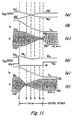
- LC resonant circuit 22 tends to introduce an undesirable delay into the change of the heights of the modulation envelope of voltage V1 and current i1, as will now be explained. Assume, for explanatory purposes, that control circuit 126 does not compensate for such undesirable delay.
- the envelope 41a′ and 41b′ of control voltage V eQ3 of FIGURE 11a decreases to zero height at time T3, the center of the vertical retrace interval, when vertical deflection current i V of FIGURES 11b and 11e is zero.
- the line rate modulation of deflection current i V and voltage V eQ3 is omitted from illustration in FIGURE 11.
- the envelope 47a′ and 47b′ of oscillatory voltage V1 of FIGURE 11c does not decrease to zero height until the later instant T5.
- the height of the modulation envelope of oscillatory V1 has not reached its proper value by time T6, the beginning of the vertical trace interval.
- the envelope height is still increasing rather than decreasing for a significant number of raster lines after the start of vertical trace.
- the raster lines scanned at the start of vertical trace will have incorrect amounts of north-south pincushion correction.
- control circuit 126 of FIGURE 3 provides delay compensation to control voltage V eQ3 to insure that the modulation envelope of oscillatory voltage V1 achieves its proper height at the beginning of the vertical trace interval.
- control circuit 126 changes the phase and modifies the amplitude variation of line rate control voltage 133H during the vertical retrace interval.
- the crossover of the modulation envelope of oscillatory voltage V1 is thereby advanced to the instant T2 of FIGURE 11f, prior to the center of the vertical retrace interval at time T3.
- the output of a comparator U2B is coupled to the output of control switch U2A and the output of a comparator U2D is coupled via a capacitor C19 and a diode D3 to the output of control switch U2C.
- a resistor R56 is coupled between ground and the junction of capacitor C19 and diode D3.
- Vertical sawtooth control voltage V D is differentiated by an RC network comprising resistors R44 and R47 and capacitors C12 and C13. The differentiated voltage developed across resistor R47 is applied to the inverting input terminal of comparator U2B and to the noninverting input terminal of comparator U2D.
- control voltage V D is a sharply sloped, positive going, sawtooth signal.
- the differentiation of voltage V D therefore produces a relatively large positive voltage across resistor R47 during the vertical retrace interval and a much smaller negative voltage during the vertical trace interval.
- comparator U2D is in saturation and discharges capacitor C19 through resistor R56.
- Diode D3 is reverse biased and disconnects comparator U2D from control switch U2C.
- the differentiated voltage across resistor R47 cuts off comparator U2D.
- Capacitor C19 charges from the +25V source through resistor R55 and resistor R56.
- the major portion of the charge current from capacitor C19 passes through diode D3 and then divides between the output of control switch U2C and resistor R41.
- the charge current of capacitor C19 passes through resistor R41 when control switch U2C is cut off, and is bypassed to ground when control switch U2C is conductive.
- the charge current of capacitor C19 produces a positive voltage drop across resistor R41 which adds to the positive going sequence of voltage levels of waveform 128H during vertical retrace. The added voltage is highest at time T1 of FIGURE 11d and ceases towards time T4 when the charge current of capacitor C19 decreases to zero.
- comparators U2B and U2D The result of the above explained operation of comparators U2B and U2D is that envelope portion 41a of FIGURE 11d is switched to zero during the interval T1 to T6 and that an extra voltage, decreasing in amplitude, is added to the original envelope portion 41b from time T1 to time T4.
- control voltage 133H has the same phase during all of vertical retrace as it has at the beginning of the subsequent vertical trace interval.
- line rate excitation current pulses i Q4 are produced with the same phase that they have at the start of vertical trace.
- the excitation current pulses i Q4 during vertical retrace develop an oscillatory voltage V1, illustrated in FIGURE 11f that has an envelope 47a and 47b that decreases to zero height substantially faster than the coresponding envelope 47a′ and 47b′ in FIGURE 11c.
- the envelope reaches the zero height point in FIGURE 11f at the advanced time T2.
- a much longer time interval, T2-T6, is available for the envelope to begin increasing in height to its value at the start of trace at time T6.
- control circuit 126 provides amplitude delay compensation to voltage V1 during vertical retrace.
- the degree of compensation is controlled by proper selection of the time constant of resistor R55 and capacitor C19 to avoid an overshoot of the line rate correction amplitude at time T6, the beginning of vertical trace.
- vertical deflection amplifier 21 may exhibit significant output impedance at the line frequency, the line rate modulation of vertical deflection current i V tends to produce a line rate component to output voltage 21V.
- Integrated circuit vertical deflection amplifiers may not permit the use of a sufficiently large supply voltage to avoid producing voltage limiting effects. The result may be a nonlinear drive at the top and bottom of field scan.
- a capacitor C18 damped by a resistor R53, advantageously tunes vertical deflection winding L V to approximately the line frequency.
- the line rate correction component of vertical deflection current i V circulates in the parallel tuned circuit formed by winding L V and capacitor C18.
- the branch of the series connected capacitor C18 and resistor R53 provides a line rate current return path. The result is that a lower magnitude line rate voltage appears at the output of vertical deflection amplifier 21.
Landscapes
- Engineering & Computer Science (AREA)
- Multimedia (AREA)
- Signal Processing (AREA)
- Details Of Television Scanning (AREA)
- Magnetic Resonance Imaging Apparatus (AREA)
- Nitrogen Condensed Heterocyclic Rings (AREA)
- Nitrogen And Oxygen Or Sulfur-Condensed Heterocyclic Ring Systems (AREA)
- Television Systems (AREA)
- Apparatus For Radiation Diagnosis (AREA)
- Outer Garments And Coats (AREA)
- Thermotherapy And Cooling Therapy Devices (AREA)
- Vessels, Lead-In Wires, Accessory Apparatuses For Cathode-Ray Tubes (AREA)
Claims (1)
- Nord-Süd-Kissenverzerrungs-Korrekturschaltung (23) für ein Fernseh-Anzeigegerät, bei dem eine Bildröhre rasterabgetastet wird, welche einen asphärischen Schirmträger (faceplate, 30) von relativ flacher Krümmung beinhaltet, welche Schaltung umfaßt:- eine Halbbild-Ablenkwicklung (Lv);- einen Halbbild-Ablenkverstärker (21) zum Erzeugen von Halbbild-Ablenkstrom in der Halbbild-Ablenkwicklung (Lv);- Mittel (22) zum Bereitstellen von Zeilenraten-Modulation des Halbbild-Ablenkstromes;- Mittel (126) zum Variieren der Hüllkurve (envelope) der Zeilenraten-Modulation des Halbbild-Ablenkstromes mit einer Zeilenrate ;gekennzeichnet durch- Mittel (138) zum nichtlinearen Signalformen der Hüllkurve, um Nord-Süd-Kissenverzerrungs-korrigierten Halbbild-Ablenkstrom zu erhalten, der eine Korrektur von verbleibender Nord-Süd-Kissenverzerrung beinhaltet, die das Rasterabtasten - in Verbindung mit der Bildröhre - begleitet.
Priority Applications (2)
| Application Number | Priority Date | Filing Date | Title |
|---|---|---|---|
| EP92116531A EP0522602B1 (de) | 1984-04-04 | 1985-04-04 | Ablenkschaltung mit Korrektur der N-S-Kissenverzerrung |
| AT88201972T ATE95019T1 (de) | 1984-04-04 | 1985-04-04 | Ablenkschaltung mit korrektur der n-skissenverzerrung. |
Applications Claiming Priority (4)
| Application Number | Priority Date | Filing Date | Title |
|---|---|---|---|
| GB8408693 | 1984-04-04 | ||
| GB848408693A GB8408693D0 (en) | 1984-04-04 | 1984-04-04 | N-s raster correction circuit |
| GB848414947A GB8414947D0 (en) | 1984-06-12 | 1984-06-12 | N-s raster correction circuit |
| GB8414947 | 1984-06-12 |
Related Parent Applications (2)
| Application Number | Title | Priority Date | Filing Date |
|---|---|---|---|
| EP85902220A Division-Into EP0176589B1 (de) | 1984-04-04 | 1985-04-04 | Ablenkschaltung mit korrektion der n-s kissenverzerrung |
| EP85902220.4 Division | 1985-04-04 |
Related Child Applications (1)
| Application Number | Title | Priority Date | Filing Date |
|---|---|---|---|
| EP92116531.2 Division-Into | 1985-04-04 |
Publications (2)
| Publication Number | Publication Date |
|---|---|
| EP0308018A1 EP0308018A1 (de) | 1989-03-22 |
| EP0308018B1 true EP0308018B1 (de) | 1993-09-22 |
Family
ID=26287562
Family Applications (3)
| Application Number | Title | Priority Date | Filing Date |
|---|---|---|---|
| EP92116531A Expired - Lifetime EP0522602B1 (de) | 1984-04-04 | 1985-04-04 | Ablenkschaltung mit Korrektur der N-S-Kissenverzerrung |
| EP88201972A Expired - Lifetime EP0308018B1 (de) | 1984-04-04 | 1985-04-04 | Ablenkschaltung mit Korrektur der N-S-Kissenverzerrung |
| EP85902220A Expired EP0176589B1 (de) | 1984-04-04 | 1985-04-04 | Ablenkschaltung mit korrektion der n-s kissenverzerrung |
Family Applications Before (1)
| Application Number | Title | Priority Date | Filing Date |
|---|---|---|---|
| EP92116531A Expired - Lifetime EP0522602B1 (de) | 1984-04-04 | 1985-04-04 | Ablenkschaltung mit Korrektur der N-S-Kissenverzerrung |
Family Applications After (1)
| Application Number | Title | Priority Date | Filing Date |
|---|---|---|---|
| EP85902220A Expired EP0176589B1 (de) | 1984-04-04 | 1985-04-04 | Ablenkschaltung mit korrektion der n-s kissenverzerrung |
Country Status (13)
| Country | Link |
|---|---|
| US (1) | US4668897A (de) |
| EP (3) | EP0522602B1 (de) |
| AT (3) | ATE95019T1 (de) |
| CA (1) | CA1263744A (de) |
| DE (3) | DE3580085D1 (de) |
| DK (1) | DK559485A (de) |
| ES (1) | ES8609816A1 (de) |
| FI (1) | FI79219C (de) |
| HK (1) | HK157295A (de) |
| PL (1) | PL146348B1 (de) |
| RU (1) | RU2011306C1 (de) |
| SG (1) | SG74548A1 (de) |
| WO (1) | WO1985004756A1 (de) |
Families Citing this family (9)
| Publication number | Priority date | Publication date | Assignee | Title |
|---|---|---|---|---|
| US4737691A (en) * | 1986-04-11 | 1988-04-12 | Rca Corporation | Television apparatus for generating a phase modulated deflection current |
| GB8706822D0 (en) * | 1987-03-23 | 1987-04-29 | Rca Corp | Active modulator circuit |
| US4972127A (en) * | 1990-04-27 | 1990-11-20 | Rca Licensing Corporation | Pincushion correction circuit with gullwing compensation |
| JPH05110888A (ja) * | 1991-10-14 | 1993-04-30 | Sony Corp | 偏向歪補正回路 |
| US5783913A (en) * | 1993-12-08 | 1998-07-21 | Thomson Consumer Electronics, Inc. | Raster distortion correction arrangement |
| DE69515022T2 (de) * | 1994-10-25 | 2000-09-14 | Koninklijke Philips Electronics N.V., Eindhoven | Ablenkkorrektur |
| JP3683969B2 (ja) * | 1996-02-20 | 2005-08-17 | 株式会社東芝 | マルチメディアテレビ受像装置 |
| US6011364A (en) * | 1996-12-04 | 2000-01-04 | Samsung Electronics Co., Ltd. | Upper and lower distortion correcting circuit by modes |
| TWI671894B (zh) * | 2014-06-26 | 2019-09-11 | 日商新力股份有限公司 | 電路基板、攝像元件及電子機器 |
Family Cites Families (20)
| Publication number | Priority date | Publication date | Assignee | Title |
|---|---|---|---|---|
| DE1247379B (de) * | 1964-09-19 | 1967-08-17 | Fernseh Gmbh | Schaltungsanordnung zur Erzeugung bogenfoermiger Stroeme |
| US3463961A (en) * | 1964-12-23 | 1969-08-26 | Sylvania Electric Prod | Raster correction circuit arrangement |
| US3320469A (en) * | 1966-09-13 | 1967-05-16 | Motorola Inc | Vertical dynamic pincushion correction circuits for television receivers |
| US3479554A (en) * | 1967-08-14 | 1969-11-18 | Motorola Inc | Raster distortion correction circuit |
| US3452243A (en) * | 1967-10-23 | 1969-06-24 | Westinghouse Electric Corp | Pincushion correction circuits |
| NL6808845A (de) * | 1968-06-22 | 1969-12-24 | ||
| NL155156B (nl) * | 1968-07-11 | 1977-11-15 | Philips Nv | Schakelinrichting voor het in een televisieweergeefinrichting opwekken van een beeldregelfrequente zaagtandvormige stroom met een rasterfrequent varierende amplitude. |
| NL6908228A (de) * | 1969-05-29 | 1970-12-01 | ||
| US3566181A (en) * | 1969-06-16 | 1971-02-23 | Zenith Radio Corp | Pin-cushion correction circuit |
| FR2083963A5 (de) * | 1970-03-11 | 1971-12-17 | Rca Corp | |
| US3825793A (en) * | 1970-06-05 | 1974-07-23 | Rca Corp | Raster correction circuit utilizing a parabolically varying load circuit |
| US3700958A (en) * | 1971-03-05 | 1972-10-24 | Rca Corp | Deflection and pincushion correction circuit |
| US3916254A (en) * | 1974-02-13 | 1975-10-28 | Warwick Electronics Inc | Adjustable pincushion correction circuit |
| US3995196A (en) * | 1974-11-04 | 1976-11-30 | Zenith Radio Corporation | Low level pincushion correction circuit |
| US3983450A (en) * | 1975-02-26 | 1976-09-28 | Zenith Radio Corporation | Low level pincushion correction system with a dual impedance yoke |
| US4041354A (en) * | 1975-10-02 | 1977-08-09 | Rca Corporation | Pincushion correction circuit |
| GB1574726A (en) * | 1976-03-19 | 1980-09-10 | Rca Corp | Side pincushion distortion correction circuit |
| US4093895A (en) * | 1976-05-03 | 1978-06-06 | Gte Sylvania Incorporated | Assymetric top-bottom pincushion correction circuit |
| US4254365A (en) * | 1979-10-01 | 1981-03-03 | Rca Corporation | Side pincushion correction modulator circuit |
| US4305023A (en) * | 1980-07-07 | 1981-12-08 | Rca Corporation | Raster distortion corrected deflection circuit |
-
1985
- 1985-04-02 US US06/719,227 patent/US4668897A/en not_active Expired - Lifetime
- 1985-04-03 CA CA000478294A patent/CA1263744A/en not_active Expired
- 1985-04-03 ES ES541956A patent/ES8609816A1/es not_active Expired
- 1985-04-04 DE DE8585902220T patent/DE3580085D1/de not_active Expired - Lifetime
- 1985-04-04 AT AT88201972T patent/ATE95019T1/de not_active IP Right Cessation
- 1985-04-04 WO PCT/US1985/000571 patent/WO1985004756A1/en active IP Right Grant
- 1985-04-04 DE DE3588160T patent/DE3588160T2/de not_active Expired - Fee Related
- 1985-04-04 DE DE88201972T patent/DE3587594T2/de not_active Expired - Fee Related
- 1985-04-04 AT AT92116531T patent/ATE155306T1/de not_active IP Right Cessation
- 1985-04-04 SG SG1996002391A patent/SG74548A1/en unknown
- 1985-04-04 EP EP92116531A patent/EP0522602B1/de not_active Expired - Lifetime
- 1985-04-04 PL PL1985252774A patent/PL146348B1/pl unknown
- 1985-04-04 AT AT85902220T patent/ATE57451T1/de not_active IP Right Cessation
- 1985-04-04 EP EP88201972A patent/EP0308018B1/de not_active Expired - Lifetime
- 1985-04-04 EP EP85902220A patent/EP0176589B1/de not_active Expired
- 1985-12-02 FI FI854762A patent/FI79219C/fi not_active IP Right Cessation
- 1985-12-03 RU SU853997405A patent/RU2011306C1/ru active
- 1985-12-03 DK DK559485A patent/DK559485A/da not_active Application Discontinuation
-
1995
- 1995-10-05 HK HK157295A patent/HK157295A/xx not_active IP Right Cessation
Also Published As
| Publication number | Publication date |
|---|---|
| CA1263744A (en) | 1989-12-05 |
| DE3588160D1 (de) | 1997-08-14 |
| EP0522602A3 (en) | 1993-03-24 |
| SG74548A1 (en) | 2000-08-22 |
| WO1985004756A1 (en) | 1985-10-24 |
| EP0176589A1 (de) | 1986-04-09 |
| DE3588160T2 (de) | 1998-01-08 |
| RU2011306C1 (ru) | 1994-04-15 |
| ATE155306T1 (de) | 1997-07-15 |
| EP0176589B1 (de) | 1990-10-10 |
| ATE57451T1 (de) | 1990-10-15 |
| DK559485D0 (da) | 1985-12-03 |
| FI854762A (fi) | 1985-12-02 |
| US4668897A (en) | 1987-05-26 |
| EP0522602A2 (de) | 1993-01-13 |
| PL252774A1 (en) | 1985-11-05 |
| FI79219B (fi) | 1989-07-31 |
| ES541956A0 (es) | 1986-09-01 |
| PL146348B1 (en) | 1989-01-31 |
| FI79219C (fi) | 1989-11-10 |
| EP0308018A1 (de) | 1989-03-22 |
| HK157295A (en) | 1995-10-13 |
| ATE95019T1 (de) | 1993-10-15 |
| DE3587594T2 (de) | 1994-04-07 |
| FI854762A0 (fi) | 1985-12-02 |
| DK559485A (da) | 1985-12-03 |
| DE3587594D1 (de) | 1993-10-28 |
| EP0176589A4 (de) | 1986-04-15 |
| DE3580085D1 (de) | 1990-11-15 |
| ES8609816A1 (es) | 1986-09-01 |
| EP0522602B1 (de) | 1997-07-09 |
Similar Documents
| Publication | Publication Date | Title |
|---|---|---|
| EP0201336B1 (de) | Schaltung zur Korrektur von Rasterverzerrungen | |
| EP0194817B1 (de) | Korrektur der Rasterverzerrung für ein eine Rechteckflachbildröhre enthaltendes Videosichtgerät | |
| EP0308018B1 (de) | Ablenkschaltung mit Korrektur der N-S-Kissenverzerrung | |
| KR840001292B1 (ko) | 라스터 왜곡 교정 편향 회로 | |
| KR960004007B1 (ko) | 내부 기하 왜곡 보정을 구비한 편향 장치 | |
| US4682085A (en) | Gullwing distortion corrected deflection circuitry for a square-planar picture tube | |
| US4644230A (en) | Focus voltage circuit for television apparatus | |
| KR950009649B1 (ko) | 라인 편향회로 | |
| US3748531A (en) | Circuit arrangement for generating in a picture display device a sawtooth current of line frequency having an amplitude varying at field frequency | |
| CA1202120A (en) | Inductorless pincushion correction circuit | |
| EP0185082B1 (de) | Ablenkschaltung für flache viereckige bildröhre mit korrigierter möwenflügelförmiger verzerrung | |
| US4777412A (en) | Gullwing distortion correction circuit | |
| JP3366327B2 (ja) | 陰極線管のスクリーン上の幾何学ひずみを補正する方法および装置 | |
| EP0284348B1 (de) | Schaltung zur Korrektur der Möwenflügelverzerrung | |
| JPH07114456B2 (ja) | 上下ピンクツシヨン修正偏向回路 | |
| JPS63125059A (ja) | 偏向装置 | |
| JPH11252395A (ja) | 電力供給変調偏向装置 | |
| JPH0377709B2 (de) | ||
| JPS597270B2 (ja) | コンバ−ゼンス又はビ−ムスポット補正回路 | |
| JPH07212614A (ja) | 画像歪補正装置 | |
| JPH02312444A (ja) | 画像歪補正装置 |
Legal Events
| Date | Code | Title | Description |
|---|---|---|---|
| PUAI | Public reference made under article 153(3) epc to a published international application that has entered the european phase |
Free format text: ORIGINAL CODE: 0009012 |
|
| 17P | Request for examination filed |
Effective date: 19881011 |
|
| AC | Divisional application: reference to earlier application |
Ref document number: 176589 Country of ref document: EP |
|
| AK | Designated contracting states |
Kind code of ref document: A1 Designated state(s): AT DE FR GB IT SE |
|
| 17Q | First examination report despatched |
Effective date: 19910814 |
|
| RAP1 | Party data changed (applicant data changed or rights of an application transferred) |
Owner name: RCA THOMSON LICENSING CORPORATION |
|
| GRAA | (expected) grant |
Free format text: ORIGINAL CODE: 0009210 |
|
| AC | Divisional application: reference to earlier application |
Ref document number: 176589 Country of ref document: EP |
|
| AK | Designated contracting states |
Kind code of ref document: B1 Designated state(s): AT DE FR GB IT SE |
|
| REF | Corresponds to: |
Ref document number: 95019 Country of ref document: AT Date of ref document: 19931015 Kind code of ref document: T |
|
| XX | Miscellaneous (additional remarks) |
Free format text: TEILANMELDUNG 92116531.2 EINGEREICHT AM 04/04/85. |
|
| REF | Corresponds to: |
Ref document number: 3587594 Country of ref document: DE Date of ref document: 19931028 |
|
| ITF | It: translation for a ep patent filed | ||
| ET | Fr: translation filed | ||
| PLBE | No opposition filed within time limit |
Free format text: ORIGINAL CODE: 0009261 |
|
| STAA | Information on the status of an ep patent application or granted ep patent |
Free format text: STATUS: NO OPPOSITION FILED WITHIN TIME LIMIT |
|
| 26N | No opposition filed | ||
| EAL | Se: european patent in force in sweden |
Ref document number: 88201972.2 |
|
| PGFP | Annual fee paid to national office [announced via postgrant information from national office to epo] |
Ref country code: DE Payment date: 20010529 Year of fee payment: 17 |
|
| REG | Reference to a national code |
Ref country code: GB Ref legal event code: IF02 |
|
| PG25 | Lapsed in a contracting state [announced via postgrant information from national office to epo] |
Ref country code: DE Free format text: LAPSE BECAUSE OF NON-PAYMENT OF DUE FEES Effective date: 20021101 |
|
| PGFP | Annual fee paid to national office [announced via postgrant information from national office to epo] |
Ref country code: SE Payment date: 20040331 Year of fee payment: 20 |
|
| PGFP | Annual fee paid to national office [announced via postgrant information from national office to epo] |
Ref country code: GB Payment date: 20040402 Year of fee payment: 20 |
|
| PGFP | Annual fee paid to national office [announced via postgrant information from national office to epo] |
Ref country code: FR Payment date: 20040421 Year of fee payment: 20 |
|
| PGFP | Annual fee paid to national office [announced via postgrant information from national office to epo] |
Ref country code: AT Payment date: 20040423 Year of fee payment: 20 |
|
| PG25 | Lapsed in a contracting state [announced via postgrant information from national office to epo] |
Ref country code: GB Free format text: LAPSE BECAUSE OF EXPIRATION OF PROTECTION Effective date: 20050403 |
|
| REG | Reference to a national code |
Ref country code: GB Ref legal event code: PE20 |
|
| EUG | Se: european patent has lapsed |